

Page 1
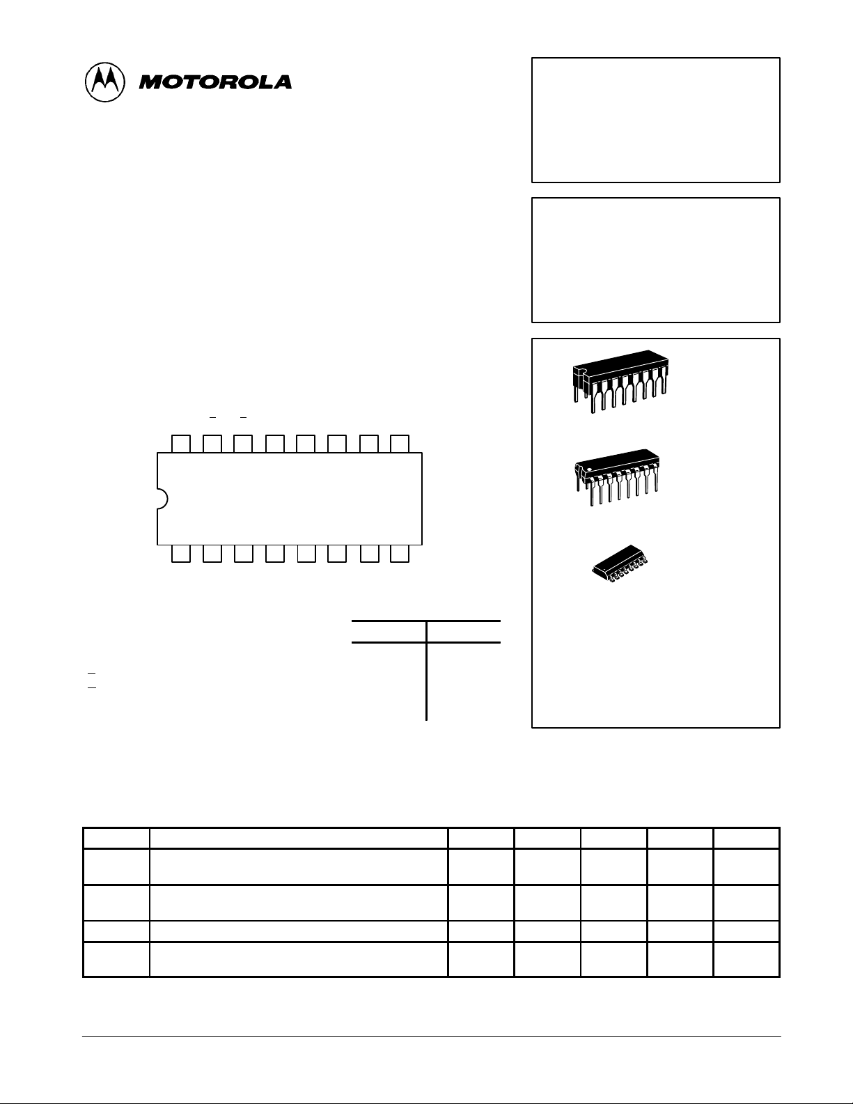
8-BIT ADDRESSABLE LATCH
The SN54/74LS259 is a high-speed 8-Bit Addressable Latch designed for
general purpose storage applications in digital systems. It is a multifunctional
device capable of storing single line data in eight addressable latches, and
also a 1-of-8 decoder and demultiplexer with active HIGH outputs. The device
also incorporates an active LOW common Clear for resetting all latches, as
well as, an active LOW Enable.
• Serial-to-Parallel Conversion
• Eight Bits of Storage With Output of Each Bit Available
• Random (Addressable) Data Entry
• Active High Demultiplexing or Decoding Capability
• Easily Expandable
• Common Clear
CONNECTION DIAGRAM DIP (TOP VIEW)
V
CC
16 15
E DQ
C
14 13 12 11 10 9
7
Q
6
Q
5
Q
4
SN54/74LS259
8-BIT ADDRESSABLE LA TCH
LOW POWER SCHOTTKY
J SUFFIX
CERAMIC
16
1
16
1
CASE 620-09
N SUFFIX
PLASTIC
CASE 648-08
123456
A
A
Q
Q
A
1
2
o
PIN NAMES LOADING (Note a)
A0, A1, A2Address lnputs 0.5 U.L. 0.25 U.L.
D Data Input 0.5 U.L. 0.25 U.L.
E Enable (Active LOW) Input 1.0 U.L. 0.5 U.L.
C Clear (Active LOW) input 0.5 U.L. 0.25 U.L.
Q0 to Q
NOTES:
a) 1 TTL Unit Load (U.L.) = 40 µA HIGH/1.6 mA LOW.
b) The Output LOW drive factor is 2.5 U.L. for Military (54) and 5 U.L. for Commercial
(74) T emperature Ranges.
Parallel Latch Outputs (Note b) 10 U.L. 5 (2.5) U.L.
7
0
1
Q
2
7
Q
GND
3
HIGH
8
16
1
LOW
D SUFFIX
SOIC
CASE 751B-03
ORDERING INFORMATION
SN54LSXXXJ Ceramic
SN74LSXXXN Plastic
SN74LSXXXD SOIC
GUARANTEED OPERATING RANGES
Symbol Parameter Min Typ Max Unit
V
T
I
I
CC
A
OH
OL
Supply Voltage 54
74
Operating Ambient Temperature Range 54
74
Output Current — High 54, 74 –0.4 mA
Output Current — Low 54
74
4.5
4.75
–55
0
5.0
5.0
25
25
5.5
5.25
125
70
4.0
8.0
V
°C
mA
FAST AND LS TTL DAT A
5-1
Page 2
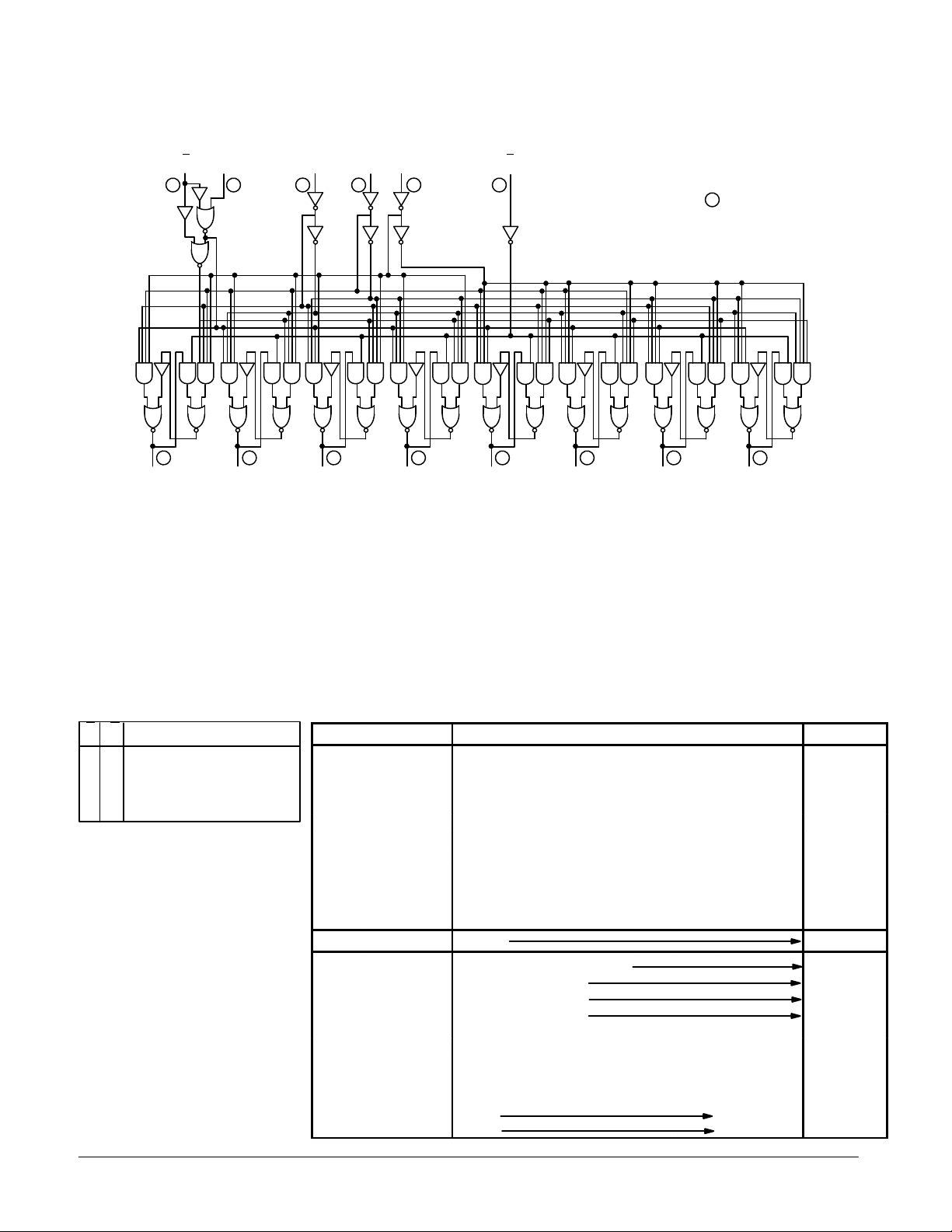
LOGIC DIAGRAM
SN54/74LS259
E DA
14 12
45 9 11 1210
Q
0
13 15
Q
1
0
Q
A
A
1
2
3
67
2
Q
3
FUNCTIONAL DESCRIPTION
The SN54/74LS259 has four modes of operation as shown
in the mode selection table. In the addressable latch mode,
data on the Data line (D) is written into the addressed
latch.The addressed latch will follow the data input with all
non-addressed latches remaining in their previous states. In
the memory mode, all latches remain in their previous state
and are unaffected by the Data or Address inputs.
In the one-of-eight decoding or demultiplexing mode, the
C
Q
4
Q
5
Q
VCC = PIN 16
GND = PIN 8
= PIN NUMBERS
6
Q
7
addressed output will follow the state of the D input with all
other inputs in the LOW state. In the clear mode all outputs are
LOW and unaffected by the address and data inputs.
When operating the SN54/74LS259 as an addressable
latch, changing more then one bit of the address could impose
a transient wrong address. Therefore, this should only be
done while in the memory mode.
The truth table below summarizes the operations.
MODE SELECTION
E
C MODE
L
H
H
L
H
X = Don’t Care Condition
L = LOW Voltage Level
H = HIGH Voltage Level
Q
Addressable Latch
H
Memory
L
Active HIGH Eight-Channel
Demultiplexer
L
Clear
= Previous Output State
N–1
TRUTH TABLE
PRESENT OUTPUT STATES
C E D A0A1A2Q
L H X X X X L L L L L L L L Clear
L LL L L L L L L L L L L L Demultiplex
L LH L L L H LLLLLLL
LLL H L L L LLLLLLL
LLH H L L L HLLLLLL
••• • •
••• • •
••• • •
••• • •
••• • •
LLH H H H L LLLLLLH
HHXXXXQ
H I I L L L L Q
H LH L L L H Q
H LL H L L Q
H LH H L L Q
• •• • •
••• • •
••• • •
••• • •
••• • •
HLL H H H Q
H L H H H H Q
Q
0
1
N–1
N–1QN–1QN–1
N–1QN–1
N–1
N–1
N–1
N–1
LQ
HQ
Q
N–1
N–1
Q
3
Q4Q
2
Q
6
N–1
N–1
Q
H
5
Q
Q
7
L
MODE
Memory
Addressable
Latch
FAST AND LS TTL DATA
5-2
Page 3
SN54/74LS259
VILI
LOW Volt
V
pg
VOHOutput HIGH Volt
CC
,
OH
,
IN IH
VOLOutput LOW Volt
V
V
V
IIHI
HIGH C
t
L
p
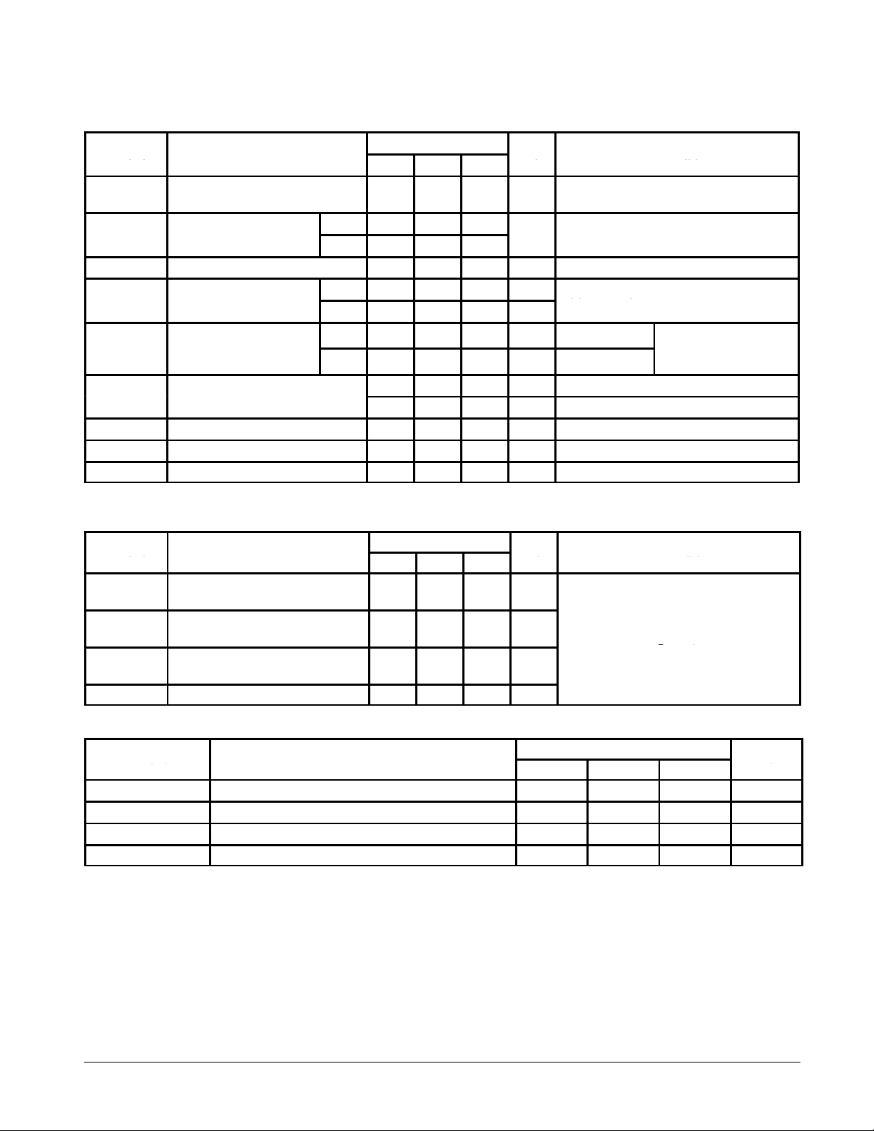
DC CHARACTERISTICS OVER OPERATING TEMPERATURE RANGE (unless otherwise specified)
Limits
Symbol Parameter
V
IH
V
IK
I
IL
I
OS
I
CC
Note 1: Not more than one output should be shorted at a time, nor for more than 1 second.
Input HIGH Voltage 2.0 V
nput
Input Clamp Diode Voltage –0.65 –1.5 V VCC = MIN, IIN = –18 mA
nput
Input LOW Current –0.4 mA VCC = MAX, VIN = 0.4 V
Short Circuit Current (Note 1) –20 –100 mA VCC = MAX
Power Supply Current 36 mA VCC = MAX
age
age
age
urren
54
74
54 2.5 3.5 V
74 2.7 3.5 V
54, 74 0.25 0.4 V IOL = 4.0 mA
74 0.35 0.5 V IOL = 8.0 mA
Min Typ Max
0.7
0.8
20 µA VCC = MAX, VIN = 2.7 V
0.1 mA VCC = MAX, VIN = 7.0 V
Unit Test Conditions
Guaranteed Input HIGH Voltage for
All Inputs
Guaranteed Input LOW Voltage for
All Inputs
VCC = MIN, IOH = MAX, VIN = V
or VIL per Truth Table
IH
VCC = VCC MIN,
=
or
IN
IL
per Truth Table
IH
AC CHARACTERISTICS (T
Symbol Parameter
t
PLH
t
PHL
t
PLH
t
PHL
t
PLH
t
PHL
t
PHL
Turn-Off Delay, Enable to Output
Turn-On Delay, Enable to Output
Turn-Off Delay, Data to Output
Turn-On Delay, Data to Output
Turn-Off Delay, Address to Output
Turn-On Delay, Address to Output
Turn-On Delay, Clear to Output 17 27 ns
AC SET-UP REQUIREMENTS (T
Symbol Parameter
t
s
t
W
t
h
t
h
= 25°C, VCC = 5.0 V)
A
= 25°C, VCC = 5.0 V)
A
Input Setup Time 20 ns
Pulse Width, Clear or Enable 15 ns
Hold Time, Data 5.0 ns
Hold Time, Address 20 ns
Limits
Min Typ Max
22
15
20
13
24
18
35
24
32
21
38
29
Unit Test Conditions
ns
ns
ns
ns
ns
ns
Limits
Min Typ Max
CL = 15 pF
Unit
FAST AND LS TTL DATA
5-3
Page 4
SN54/74LS259
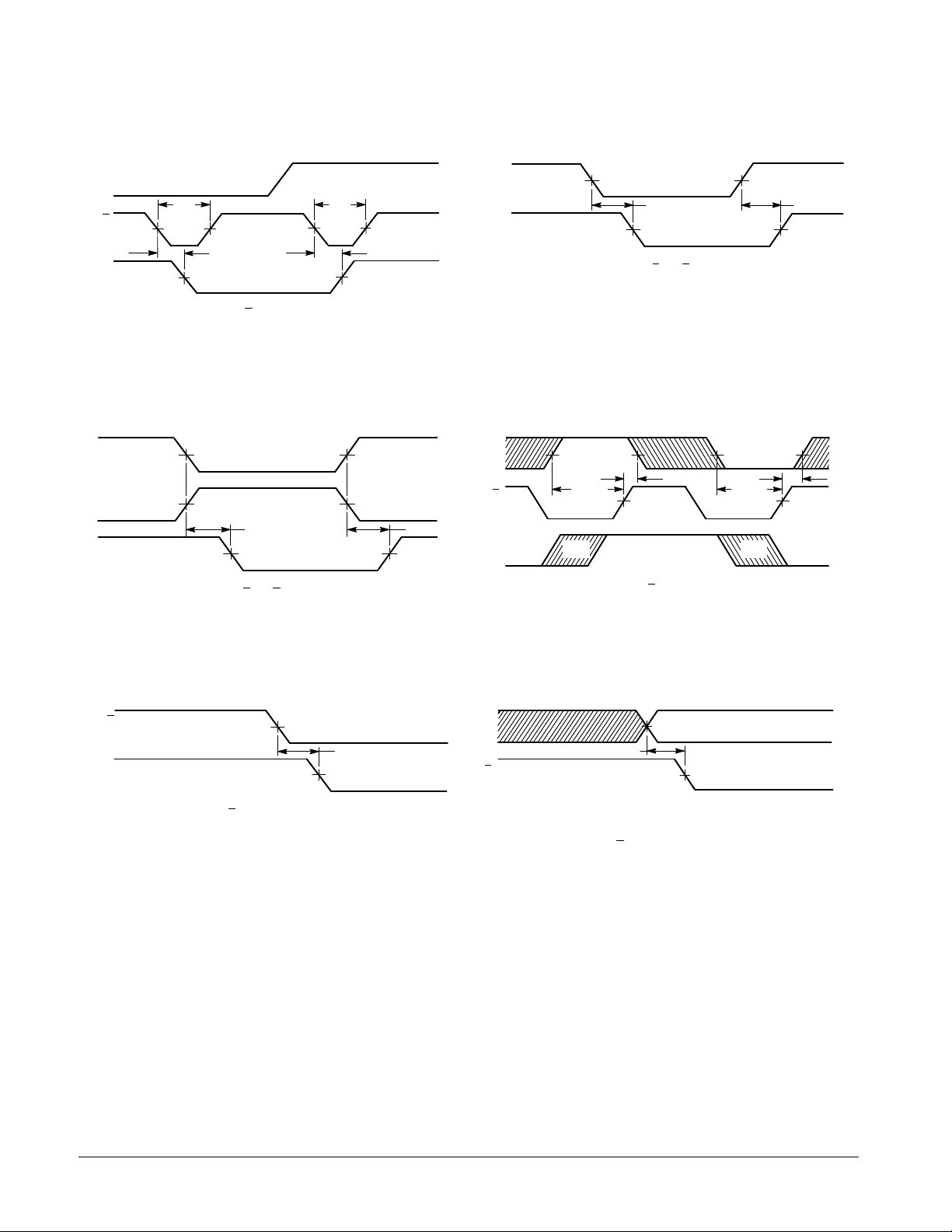
AC WAVEFORMS
D
t
w
E
t
PHL
Q
OTHER CONDITIONS: C = H, A = STABLE
t
PLH
t
w
1.3 V
Figure 1. T urn-on and Turn-off Delays, Enable To
Output and Enable Pulse Width
A
1
A
1
Q
1
OTHER CONDITIONS: E
1.3 V
1.3 V
1.3 V
1.3 V
t
PHL
1.3 V 1.3 V
= L, C = L, D = H
Figure 3. T urn-on and Turn-off Delays,
Address to Output
1.3 V
t
PLH
D
Q
OTHER CONDITIONS: E
1.3 V 1.3 V
t
PHL
= L, C = H, A = STABLE
Figure 2. T urn-on and Turn-off Delays,
Data to Output
D
E
Q
ts(H)
Q=D Q=D
OTHER CONDITIONS: C
th(H) th(L)
= H, A = STABLE
ts(L)
Figure 4. Setup and Hold Time, Data to Enable
t
PLH
1.3 V1.3 V
1.3 V
C
Q
OTHER CONDITIONS: E = H
Figure 5. Turn-on Delay, Clear to Output
1.3 V
t
PHL
1.3 V
A
E
OTHER CONDITIONS: C
t
s
= H
STABLE ADDRESS
Figure 6. Setup Time, Address to Enable
(See Notes 1 and 2)
NOTES:
1. The Address to Enable Setup Time is the time before the HIGH-to-LOW Enable transition that the Address must be stable so that the correct latch is
addressed and the other latches are not affected.
2. The shaded areas indicate when the inputs are permitted to change for predictable output performance.
FAST AND LS TTL DATA
5-4
 Loading...