

Page 1
SN54/74LS257B
QUAD 2-INPUT MULTIPLEXER
WITH 3-STATE OUTPUTS
The LSTTL / MSI SN54/ 74LS257B and the SN54 / 74LS258B are Quad
2-Input Multiplexers with 3-state outputs. Four bits of data from two sources
can be selected using a Common Data Select input. The four outputs present
the selected data in true (non-inverted) form. The outputs may be switched to
a high impedance state with a HIGH on the common Output Enable (EO) Input, allowing the outputs to interface directly with bus oriented systems. It is
fabricated with the Schottky barrier diode process for high speed and is completely compatible with all Motorola TTL families.
• Schottky Process For High Speed
• Multiplexer Expansion By Tying Outputs Together
• Non-Inverting 3-State Outputs
• Input Clamp Diodes Limit High Speed Termination Effects
• Special Circuitry Ensures Glitch Free Multiplexing
• ESD > 3500 Volts
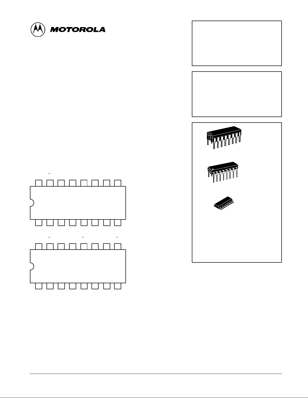
CONNECTION DIAGRAM DIP (TOP VIEW)
I
V
CC
16 15
E
0I0cI1cZc
14 13 12 11 10 9
I
0d
1d
Z
d
SN54/74LS258B
QUAD 2-INPUT MULTIPLEXER
WITH 3-STATE OUTPUTS
LOW POWER SCHOTTKY
J SUFFIX
CERAMIC
16
1
16
1
CASE 620-09
N SUFFIX
PLASTIC
CASE 648-08
SN54/74LS257B
123456
I0aI
S
V
CC
16 15
1aZaI0bI1bZb
E
0I0cI1cZc
14 13 12 11 10 9
I
0d
SN54/74LS258B
123456
I0aI
S
Z
aI0bI1bZb
1a
7
I
1d
7
8
GND
Z
d
8
GND
VCC = PIN 16
GND = PIN 8
NOTE:
The Flatpak version
has the same pinouts
(Connection Diagram) as
the Dual In-Line Package.
D SUFFIX
16
1
SOIC
CASE 751B-03
ORDERING INFORMATION
SN54LSXXXJ Ceramic
SN74LSXXXN Plastic
SN74LSXXXD SOIC
FAST AND LS TTL DAT A
5-1
Page 2
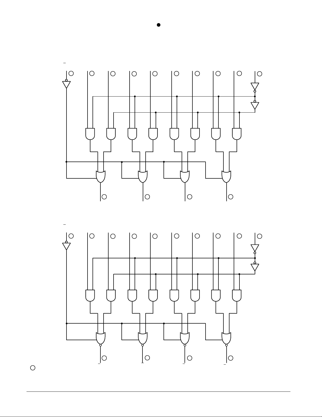
LOGIC DIAGRAMS
E
0
SN54/74LS257B D SN54/74LS258B
SN54/74LS257B
I
0a
15
I
1a
2
I
0b
3
I
1b
5
I
0c
6
I
1c
14
I
0d
13
I
1d
11
S
10
1
4
Z
a
7
Z
b
12
Z
c
9
Z
d
SN54/74LS258B
E
0
I
0a
15
I
1a
2
I
0b
3
I
1b
5
I
0c
6
I
1c
14
I
0d
13
I
1d
11
S
10
1
VCC = PIN 16
GND = PIN 8
= PIN NUMBERS
4 912
Z
a
7
Z
b
FAST AND LS TTL DATA
5-2
Z
c
Z
d
Page 3
SN54/74LS257B D SN54/74LS258B
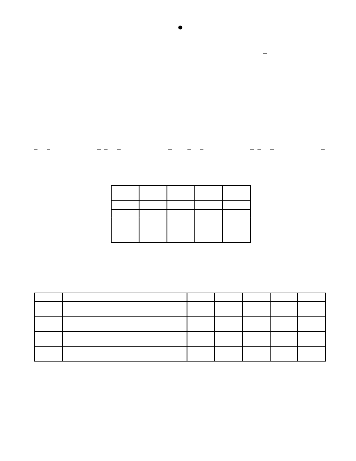
FUNCTIONAL DESCRIPTION
The LS257B and LS258B are Quad 2-Input Multiplexers
with 3-state outputs. They select four bits of data from two
sources each under control of a Common Data Select Input.
When the Select Input is LOW, the I0 inputs are selected and
when Select is HIGH, the I1 inputs are selected. The data on
the selected inputs appears at the outputs in true (noninverted) form for the LS257B and in the inverted form for the
LS258B.
The LS257B and LS258B are the logic implementation of a
4-pole, 2-position switch where the position of the switch is
determined by the logic levels supplied to the Select Input. The
logic equations for the outputs are shown below:
When the Output Enable Input (E
) is HIGH, the outputs are
0
forced to a high impedance “off” state. If the outputs are tied
together, all but one device must be in the high impedance
state to avoid high currents that would exceed the maximum
ratings. Designers should ensure that Output Enable signals
to 3-state devices whose outputs are tied together are
designed so there is no overlap.
LS257B
Za = E
Z
• (I1a • S + I0a • S
0
= E0 • (I1c • S + I0c • S
c
) Zb = E
) Z
• (I1b • S + I0b • S
0
= E0 • (I1d • S + I0d • S
d
LS258B
Z
)
)
= E0 • (I1a • S + I0a • S
a
Z
= E0 • (I1c • S + I0c • S
c
) Z
= E0 • (I1b • S + I0b • S
b
) Z
= E0 • (I1d • S + I0d • S
d
TRUTH TABLE
OUTPUT
ENABLE
E
O
H X X X (Z) (Z)
L H X LL H
L H XHH L
L L LXL H
L L HXH L
H = HIGH Voltage Level
L = LOW Voltage Level
X = Don’t Care
(Z) = High Impedance (off)
SELECT
INPUT
S I
DATA
INPUTS
0I1
OUTPUTS
LS257B
Z Z
OUTPUTS
LS258B
GUARANTEED OPERATING RANGES
Symbol Parameter Min Typ Max Unit
V
T
I
I
CC
A
OH
OL
Supply Voltage 54
74
Operating Ambient Temperature Range 54
74
Output Current — High 54
74
Output Current — Low 54
74
4.5
4.75
–55
0
5.0
5.0
25
25
5.5
5.25
125
70
–1.0
–2.6
12
24
)
)
V
°C
mA
mA
FAST AND LS TTL DATA
5-3
Page 4
SN54/74LS257B D SN54/74LS258B
VILI
LOW Volt
V
pg
VOHOutput HIGH Volt
CC
,
OH
,
IN IH
VOLOutput LOW Volt
V
V
V
I
IH
C
F
L
p
L
p
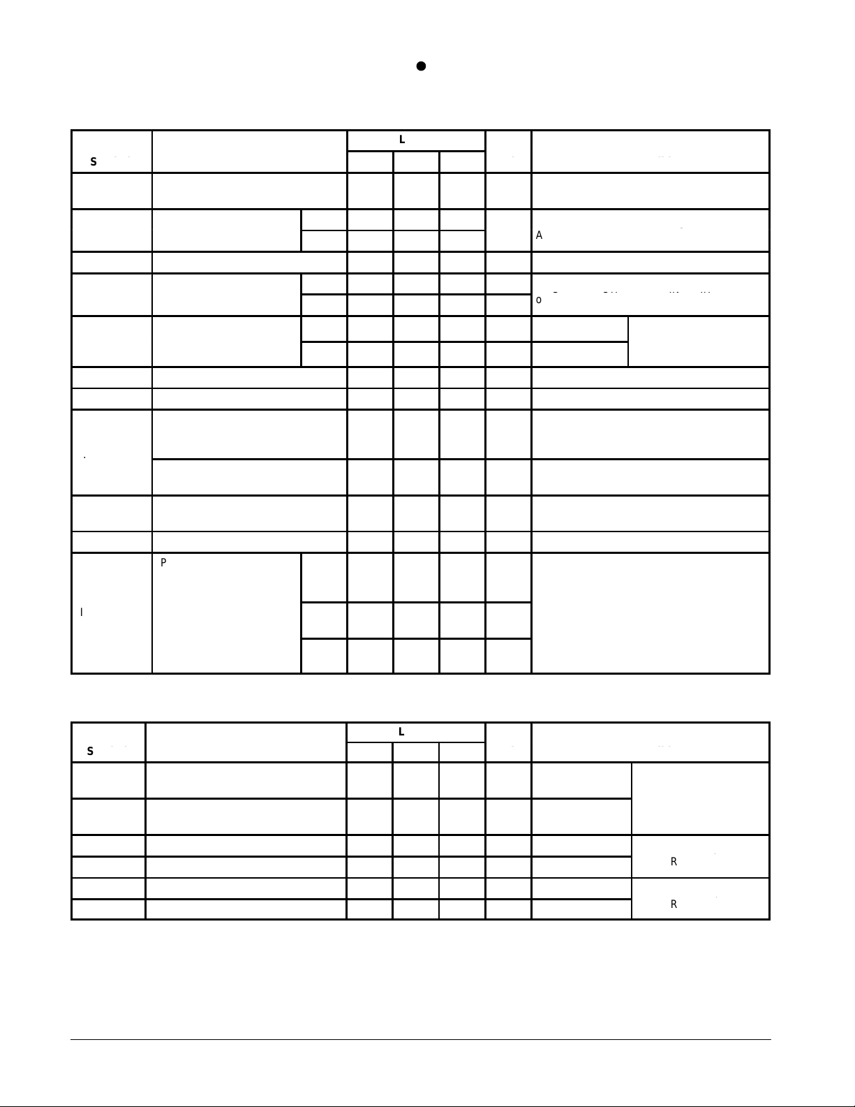
DC CHARACTERISTICS OVER OPERATING TEMPERATURE RANGE (unless otherwise specified)
Limits
Symbol Parameter
V
IH
V
IK
I
OZH
I
OZL
I
IH
I
IL
I
OS
I
CC
Note 1: Not more than one output should be shorted at a time, nor for more than 1 second.
Input HIGH Voltage 2.0 V
nput
Input Clamp Diode Voltage –0.65 –1.5 V VCC = MIN, IIN = –18 mA
Output Off Current — HIGH 20 µA VCC = MAX, V
Output Off Current — LOW –20 µA VCC = MAX, V
Input HIGH Current
Other Inputs
S Inputs
Other Inputs
S Inputs
Input LOW Current
All Inputs
Short Circuit Current (Note 1) –30 –130 mA VCC = MAX
Power Supply Current
Total, Output HIGH
Total, Output LOW
Total, Output 3-State
age
age
age
54
74
54 2.4 3.4 V
74 2.4 3.1 V
54, 74 0.25 0.4 V IOL = 12 mA
74 0.35 0.5 V IOL = 24 mA
LS257B
LS258B
LS257B
LS258B
LS257B
LS258B
Min Typ Max
0.7
0.8
20
40
0.1
0.2
–0.4 mA VCC = MAX, VIN = 0.4 V
10
9.0
16
14
19
16
Unit Test Conditions
Guaranteed Input HIGH Voltage for
All Inputs
Guaranteed Input LOW Voltage for
All Inputs
VCC = MIN, IOH = MAX, VIN = V
or VIL per Truth Table
µA VCC = MAX, VIN = 2.7 V
mA VCC = MAX, VIN = 7.0 V
mA
VCC = MAX
mA
mA
VCC = VCC MIN,
=
IN
per Truth Table
= 2.7 V
OUT
= 0.4 V
OUT
IH
or
IL
IH
AC CHARACTERISTICS (T
= 25°C, VCC = 5.0 V) See SN54LS251 for Waveforms
A
Symbol Parameter
t
PLH
t
PHL
t
PLH
t
PHL
t
PZH
t
PZL
t
PLZ
t
PHZ
Propagation Delay, Data to Output
Propagation Delay, Select to Output
Output Enable Time to HIGH Level 20 25 ns Figures 4 & 5
Output Enable Time to LOW Level 20 25 ns Figures 3 & 5
Output Disable Time to LOW Level 16 25 ns Figures 3 & 5
Output Disable Time from HIGH Level 18 25 ns Figures 4 & 5
Limits
Min Typ Max
10
12
14
14
13
15
21
21
FAST AND LS TTL DATA
5-4
Unit Test Conditions
ns Figures 1 & 2
ns Figures 1 & 2
CL = 45 pF
RL = 667 Ω
CL = 5.0 pF
RL = 667 Ω
= 45 p
L
 Loading...