

Page 1
DUAL MONOSTABLE
MULTIVIBRATORS
WITH SCHMITT-TRIGGER INPUTS
SN54/74LS221
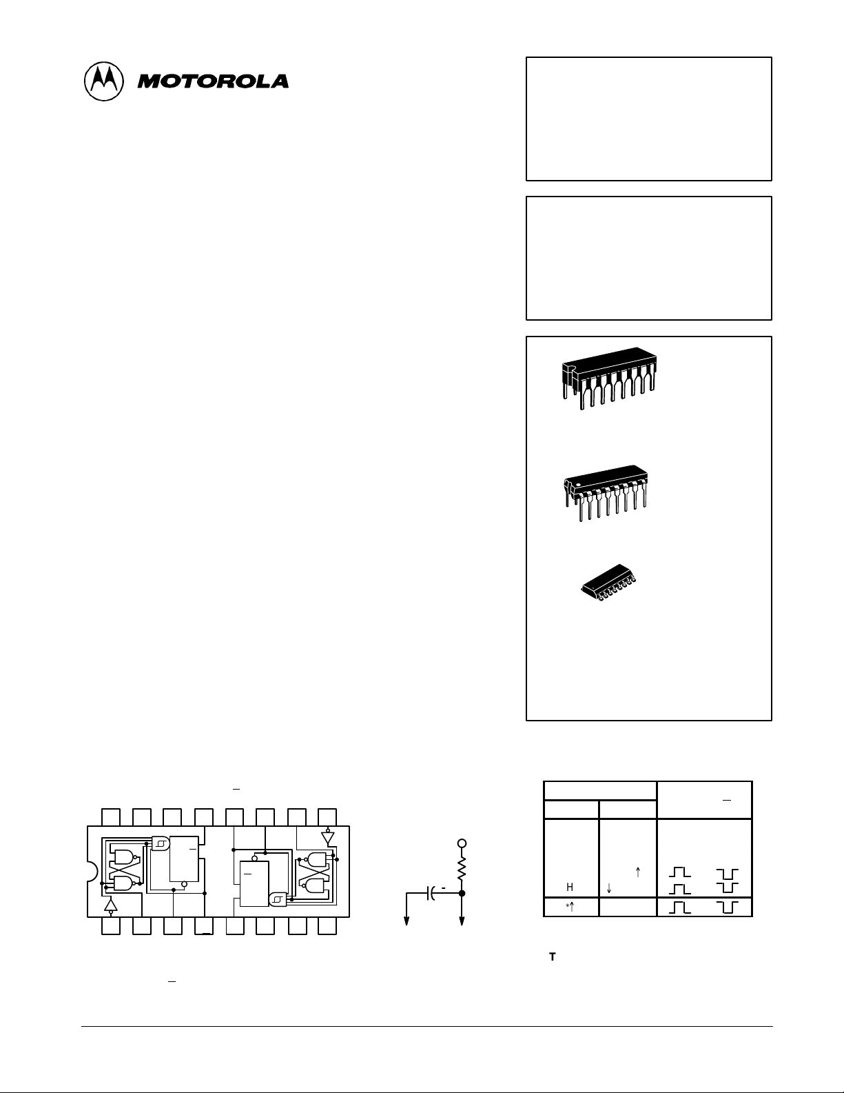
Each multivibrator of the LS221 features a negative-transition-triggered
input and a positive-transition-triggered input either of which can be used as
an inhibit input.
Pulse triggering occurs at a voltage level and is not related to the transition
time of the input pulse. Schmitt-trigger input circuitry for B input allows
jitter-free triggering for inputs as slow as 1 volt/second, providing the circuit
with excellent noise immunity . A high immunity to VCC noise is also provided
by internal latching circuitry .
Once triggered, the outputs are independent of further transitions of the
inputs and are a function of the timing components. The output pulses can be
terminated by the overriding clear. Input pulse width may be of any duration
relative to the output pulse width. Output pulse width may be varied from 35
nanoseconds to a maximum of 70 s by choosing appropriate timing
components. With R
= 2.0 kΩ and C
ext
= 0, a typical output pulse of 30
ext
nanoseconds is achieved. Output rise and fall times are independent of pulse
length.
Pulse width stability is achieved through internal compensation and is
virtually independent of VCC and temperature. In most applications, pulse
stability will only be limited by the accuracy of external timing components.
Jitter-free operation is maintained over the full temperature and VCC ranges
for greater than six decades of timing capacitance (10 pF to 10 µF), and
greater than one decade of timing resistance (2.0 to 70 kΩ for the
SN54LS221, and 2.0 to 100 kΩ for the SN74LS221). Pulse width is defined
by the relationship: tw(out) = C
if C
is in pF and R
ext
is in kΩ. If pulse cutoff is not critical, capacitance up
ext
extRext
ln 2.0
≈0.7 C
ext Rext
; where tW is in ns
to 1000 µF and resistance as low as 1.4 kΩ may be used. The range of
jitter-free pulse widths is extended if VCC is 5.0 V and 25°C temperature.
• SN54LS221 and SN74LS221 is a Dual Highly Stable One-Shot
• Overriding Clear Terminates Output Pulse
• Pin Out is Identical to SN54/74LS123
DUAL MONOSTABLE
MULTIVIBRATORS
WITH SCHMITT-TRIGGER INPUTS
LOW POWER SCHOTTKY
J SUFFIX
CERAMIC
16
1
16
1
16
1
ORDERING INFORMATION
SN54LSXXXJ Ceramic
SN74LSXXXN Plastic
SN74LSXXXD SOIC
CASE 620-09
N SUFFIX
PLASTIC
CASE 648-08
D SUFFIX
SOIC
CASE 751B-03
(TOP VIEW)
1 R
V
CC
16 15
123456
1A
positive logic: Low input to clear resets Q low and
positive logic: Q
positive logic: or B inputs.
1
ext/
C
C
ext
1B 1
1Q 2Q
ext
14 13 12 11 10 9
Q
Q
CLR
1Q
CLR
high regardless of dc levels at A
CLR
CLR
Q
Q
2Q 2
C
2
ext
2B
2 R
C
7
/
GND
ext
ext
2A
+
8
ext
FAST AND LS TTL DATA
5-1
FUNCTION TABLE
(EACH MONOSTABLE)
INPUTS OUTPUTS
CLEAR A B Q Q
L X X L H
V
CC
R
ext
R/CC
X H XL H
XXLL H
HL
H
*
°
*See operational notes — Pulse Trigger Modes
TYPE
SN54LS221 23 mW 49 s
SN74LS221 23 mW 70 s
°
±
H
LH
TYPICAL
POWER
DISSIPATION LENGTH
MAXIMUM
OUTPUT PULSE
Page 2

SN54/74LS221
OPERATIONAL NOTES
Once in the pulse trigger mode, the output pulse width is
determined by tW = R
within their minimum and maximum valves and the duty cycle
is less than 50%. This pulse width is essentially independent
of VCC and temperature variations. Output pulse widths varies
typically no more than ±0.5% from device to device.
If the duty cycle, defined as being 100• where T is the
input
period of the input pulse, rises above 50%, the output pulse
width will become shorter. If the duty cycle varies between
low and high valves, this causes the output pulse width to
vary in length, or jitter. To reduce jitter to a minimum, R
should be as large as possible. (Jitter is independent of C
With R
approaches 90%.
Although the LS221 is pin-for-pin compatible with the
LS123, it should be remembered that they are not functionally
identical. The LS123 is retriggerable so that the output is
dependent upon the input transitions once it is high. This is not
the case for the LS221. Also note that it is recommended to
externally ground the LS123 C
done on the LS221.
The SN54LS/74LS221 is a dual, monolithic, non-retriggerable, high-stability one shot. The output pulse width, tW can be
varied over 9 decades of timing by proper selection of the
external timing components, R
Pulse triggering occurs at a voltage level and is, therefore,
independent of the input slew rate. Although all three inputs
have this Schmitt-trigger effect, only the B input should be
used for very long transition triggers (≥1.0 µV/s). High
immunity to VCC noise (typically 1.5 V) is achieved by internal
latching circuitry. However, standard VCC bypassing is
strongly recommended.
The LS221 has four basic modes of operation.
= 100K, jitter is not appreciable until the duty cycle
ext
extCext
In2, as long as R
pin. However, this cannot be
ext
and C
ext
ext
and C
ext
t
W
T
.
ext
ext
are
ext
).
Clear Mode: If the clear input is held low, irregardless of
the previous output state and other input
states, the Q output is low.
Inhibit Mode: If either the A input is high or the B input is
low, once the Q output goes low , it cannot be
retriggered by other inputs.
Pulse Trigger
Mode: A transition of the A or B inputs as indicated
in the functional truth table will trigger the Q
output to go high for a duration determined
by the tW equation described above; Q
go low for a corresponding length of time.
The Clear input may also be used to trigger
an output pulse, but special logic preconditioning on the A or B inputs must be done as
follows:
Following any output triggering action
using the A or B inputs, the A input must
be set high OR the B input must be set
low to allow Clear to be used as a trigger.
Inputs should then be set up per the truth
table (without triggering the output) to
allow Clear to be used a trigger for the
output pulse.
If the Clear pin is routinely being used to
trigger the output pulse, the A or B inputs
must be toggled as described above
before and between each Clear trigger
event.
Once triggered, as long as the output
remains high, all input transitions (except
overriding Clear) are ignored.
will
Overriding
Clear Mode: If the Q output is high, it may be forced low
FAST AND LS TTL DATA
5-2
by bringing the clear input low.
Page 3
SN54/74LS221
V
gg
V
MIN
V
gg
V
MIN
VILI
LOW Volt
V
pg
VOHOutput HIGH Volt
V
MIN, I
MAX
VOLOutput LOW Volt
V
MIN
IIHI
HIGH C
t
CC
CC
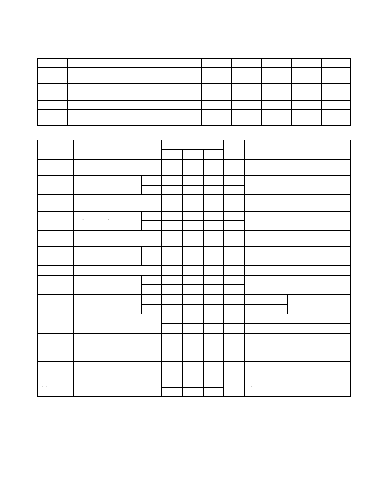
GUARANTEED OPERATING RANGES
Symbol Parameter Min Typ Max Unit
V
CC
T
A
I
OH
I
OL
DC CHARACTERISTICS OVER OPERATING TEMPERATURE RANGE (unless otherwise specified)
Symbol Parameter
V
T+
T–
V
T+
T–
V
IH
V
IK
I
IL
I
OS
I
CC
Note 1: Not more than one output should be shorted at a time, nor for more than 1 second.
Supply Voltage 54
Operating Ambient Temperature Range 54
Output Current — High 54, 74 –0.4 mA
Output Current — Low 54
Limits
Min Typ Max
Positive-Going Threshold
Voltage at C Input
Negative-Going Threshold
Voltage at C Input
Positive-Going Threshold
Voltage at B Input
Negative-Going Threshold
Voltage at B Input
Input HIGH Voltage 2.0 V
nput
Input Clamp Voltage –1.5 V VCC = MIN, IIN = –18 mA
nput
Input LOW Current
Input A
Input B
Clear
Short Circuit Current (Note 1) –20 –100 mA VCC = MAX
Power Supply Current
Quiescent
Triggered 19 27
age
age
age
urren
54 0.7 0.8 V
74
54 0.7 0.9 V
74
54 0.7
74 0.8
54 2.5 3.4 V
74 2.7 3.4 V
54 0.25 0.4 V IOL = 4.0 mA
74 0.35 0.5 V IOL = 8.0 mA
0.7 0.8 V
0.8 0.9 V
1.0 2.0 V VCC = MIN
1.0 2.0 V VCC = MIN
4.7 11
74
74
74
20 µA VCC = MAX, VIN = 2.7 V
0.1 mA VCC = MAX, VIN = 7.0 V
–0.4
–0.8
–0.8
4.5
4.75
–55
0
Unit Test Conditions
CC
CC
Guaranteed Input HIGH Voltage for
A Input
Guaranteed Input LOW Voltage for
A Input
CC
mA VCC = MAX, VIN = 0.4 V
mA VCC = MAX
=
=
=
5.0
5.0
25
25
OH
=
CC
5.5
5.25
125
70
4.0
8.0
=
V
°C
mA
FAST AND LS TTL DATA
5-3
Page 4
SN54/74LS221
From
To
t
t
C
R
Ω
L
p,
t
A
B
Q
Q
dv/dt
t
W
R
Ext
kΩ
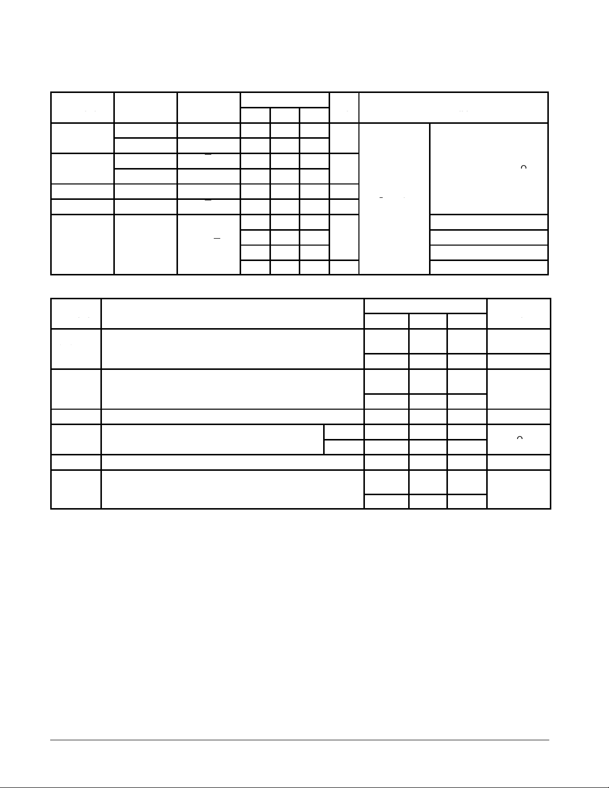
AC CHARACTERISTICS (V
From To
Symbol
PLH
PHL
t
PHL
t
PLH
W(out)
(Input)
A Q 45 70
B Q 35 55
A Q 50 80
B Q 40 65
Clear Q 35 55 ns
Clear Q 44 65 ns
or
AC SETUP REQUIREMENTS (V
Symbol Parameter
Rate of Rise or Fall of Input Pulse
dv/dt
Input Pulse Width
t
W
t
s
ext
C
ext
Clear-Inactive-State Setup Time 15 ns
ernal Timing Resistance
External Timing Capacitance 0 1000 µF
Output Duty Cycle
= 5.0 V, TA = 25°C)
CC
(Output)
or
= 5.0 V, TA = 25°C)
CC
Limits
Min Typ Max
70 120 150 C
20 47 70
600 670 750 C
6.0 6.9 7.5 ms C
Schmitt, B 1.0 V/s
Logic Input, A 1.0 V/µs
A or B, t
Clear, tW (clear) 40
RT = 2.0 kΩ 50 %
RT = MAX R
Unit Test Conditions
ns
ns
CL = 15 pF,
See Figure 1
ns
Limits
Min Typ Max
W(in)
54 1.4 70
74 1.4 100
ext
40 ns
= 80 pF,
ext
= 80 pF, R
ext
C
= 0, R
ext
= 100 pF, R
ext
= 1.0 µF, R
ext
90
= 2.0 kΩ
ext
ext
ext
ext
ext
= 2.0
= 2.0 Ω
= 10 kΩ
= 10 kΩ
Unit
FAST AND LS TTL DATA
5-4
Page 5
B INPUT
CLEAR
Q OUTPUT
Q
OUTPUT
A INPUT IS LOW.
SN54/74LS221
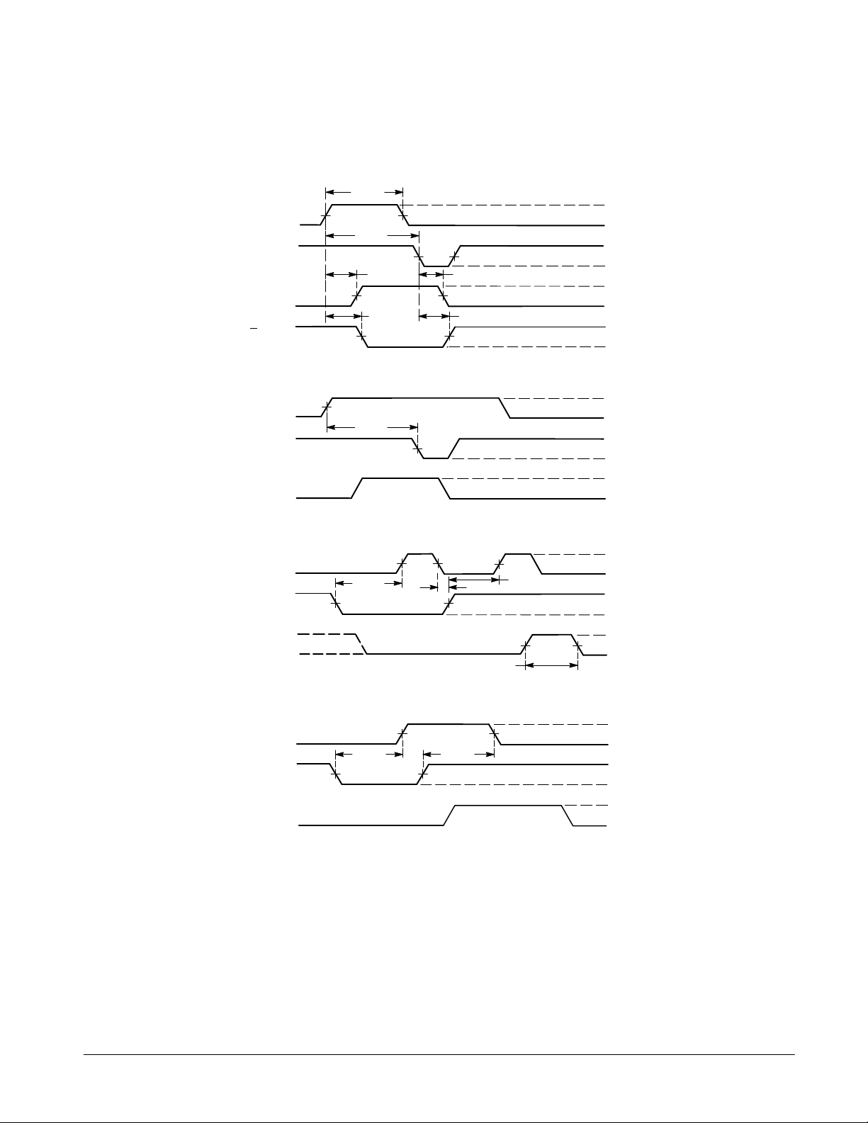
AC WAVEFORMS
t
W(in)
1.3 V
≥
60 ns
t
PLH
t
PHL
TRIGGER FROM B, THEN CLEAR — CONDITION 1
t
PHL
t
PLH
3 V
0 V
3 V
0 V
V
V
V
V
OH
OL
OH
OL
B INPUT
CLEAR
Q OUTPUT
A INPUT IS LOW.
B INPUT
CLEAR
TRIGGERED
Q OUTPUT
NOT TRIGGERED
A INPUT IS LOW.
B INPUT
CLEAR
Q OUTPUT
A INPUT IS LOW.
≥
60 ns
1.3 V
TRIGGER FROM B, THEN CLEAR — CONDITION 2
t
≥
50 ns
CLEAR OVERRIDING B, THEN TRIGGER FROM B
≥
50 ns
TRIGGERING FROM POSITIVE TRANSITION OF CLEAR
≥
1.3 V
≥
50 ns
0
t
W(out)
s
3 V
0 V
3 V
0 V
V
V
3 V
0 V
3 V
0 V
V
V
3 V
0 V
3 V
0 V
V
V
OH
OL
OH
OL
OH
OL
Figure 1
FAST AND LS TTL DATA
5-5
 Loading...