

Page 1
SN54/74LS196
4-STAGE PRESETTABLE
RIPPLE COUNTERS
The SN54/74LS196 decade counter is partitioned into divide-by-two and divide-by-five sections which can be combined to count either in BCD (8, 4, 2, 1)
sequence or in a bi-quinary mode producing a 50% duty cycle output. The
SN54/74LS197 contains divide-by-two and divide-by-eight sections which
can be combined to form a modulo-16 binary counter. Low Power Schottky
technology is used to achieve typical count rates of 70 MHz and power dissipation of only 80 mW.
Both circuit types have a Master Reset (MR
inputs and asynchronously forces all outputs LOW. A Parallel Load input (PL
overrides clocked operations and asynchronously loads the data on the Parallel Data inputs (Pn) into the flip-flops. This preset feature makes the circuits
usable as programmable counters. The circuits can also be used as 4-bit
latches, loading data from the Parallel Data inputs when PL
ing the data when PL
is HIGH.
• Low Power Consumption — Typically 80 mW
• High Counting Rates — Typically 70 MHz
• Choice of Counting Modes — BCD, Bi-Quinary , Binary
• Asynchronous Presettable
• Asynchronous Master Reset
• Easy Multistage Cascading
• Input Clamp Diodes Limit High Speed Termination Effects
) input which overrides all other
is LOW and stor-
SN54/74LS197
4-ST AGE PRESETTABLE
RIPPLE COUNTERS
LOW POWER SCHOTTKY
)
J SUFFIX
CERAMIC
14
1
14
1
CASE 632-08
N SUFFIX
PLASTIC
CASE 646-06
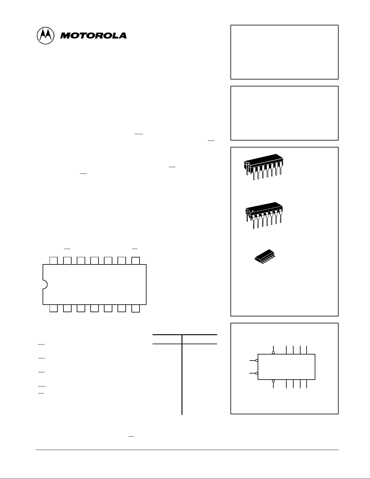
CONNECTION DIAGRAM DIP (TOP VIEW)
VCCMR
14 13 12 11 10 9
123456
PL Q2P2P0Q0CP
PIN NAMES LOADING (Note a)
CP
0
CP
(LS196) Clock (Active LOW Going Edge) 2.0 U.L. 1.75 U.L.
1
CP
(LS197) Clock (Active LOW Going Edge) 1.0 U.L. 0.8 U.L.
1
MR Master Reset (Active LOW) Input 1.0 U.L. 0.5 U.L.
PL Parallel Load (Active LOW) Input 0.5 U.L. 0.25 U.L.
P0–P
3
Q0–Q
3
NOTES:
a. 1 TTL Unit Load (U.L.) = 40µA HIGH/1.6 mA LOW.
b. The Output LOW drive factor is 2.5 U.L. for Military (54) and 5 U.L. for Commercial (74)
b. T emperature Ranges.
c. In addition to loading shown, Q0 can also drive CP
Q3P3P1Q1CP
Clock (Active LOW Going Edge) 1.0 U.L. 1.5 U.L.
Input to Divide-by-Two Section
Input to Divide-by-Five Section
Input to Divide-by-Eight Section
Data Inputs 0.5 U.L. 0.25 U.L.
Outputs (Notes b, c) 10 U.L. 5 (2.5) U.L.
1
0
8
7
GND
.
1
NOTE:
The Flatpak version
has the same pinouts
(Connection Diagram) as
the Dual In-Line Package.
HIGH
LOW
D SUFFIX
14
1
CASE 751A-02
ORDERING INFORMATION
SN54LSXXXJ Ceramic
SN74LSXXXN Plastic
SN74LSXXXD SOIC
LOGIC SYMBOL
1 4 10 3 11
CP
CP
PLMRP
0
1
8
6
P1P2P
0
Q1Q2Q
Q
0
VCC = PIN 14
GND = PIN 7
SOIC
3
3
1229513
FAST AND LS TTL DAT A
5-1
Page 2
SN54/74LS196 • SN54/74LS197
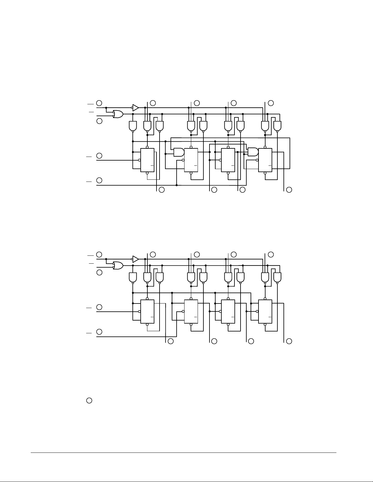
LOGIC DIAGRAM
MR
CP
CP
MR
PL
PL
P
0
4
1
S
D
Q
8
J
P
1
1013
S
D
Q
J
P
2
3
S
D
Q
J
P
3
11
S
D
Q
J
0
C
K
Q
D
6
1
5 9
Q
0
C
K
Q
D
C
K
Q
D
2
Q
1
Q
2
C
K
Q
D
12
Q
3
LS196
P
0
4
1
P
1
1013
P
2
3
P
3
11
8
CP
0
6
CP
1
VCC = PIN 14
GND = PIN 7
= PIN NUMBERS
S
D
Q
J
C
K
Q
D
5 9
Q
0
S
D
Q
J
C
K
Q
D
LS197
FAST AND LS TTL DATA
5-2
S
D
Q
J
C
K
Q
D
Q
1
S
D
Q
J
C
K
Q
D
2
Q
2
12
Q
3
Page 3
SN54/74LS196 • SN54/74LS197
RESPONSE
FUNCTIONAL DESCRIPTION
The LS196 and LS197 are asynchronously presettable decade and binary ripple counters. The LS196 Decade Counter
is partitioned into divide-by-two and divide-by-five sections
while the LS197 is partitioned into divide-by-two and divideby-eight sections, with all sections having a separate Clock input. In the counting modes, state changes are initiated by the
HIGH to LOW transition of the clock signals. State changes of
the Q outputs, however, do not occur simultaneously because
of the internal ripple delays. When using external logic to decode the Q outputs, designers should bear in mind that the unequal delays can lead to decoding spikes and thus a decoded
signal should not be used as a clock or strobe. The CP
serves the Q0 flip-flop in both circuit types while the CP
input
0
input
1
serves the divide-by-five or divide-by-eight section. The Q
output is designed and specified to drive the rated fan-out plus
the CP
Q0 driving CP
input. With the input frequency connected to CP0 and
1
, the LS197 forms a straightforward module-16
1
counter, with Q0 the least significant output and Q3 the most
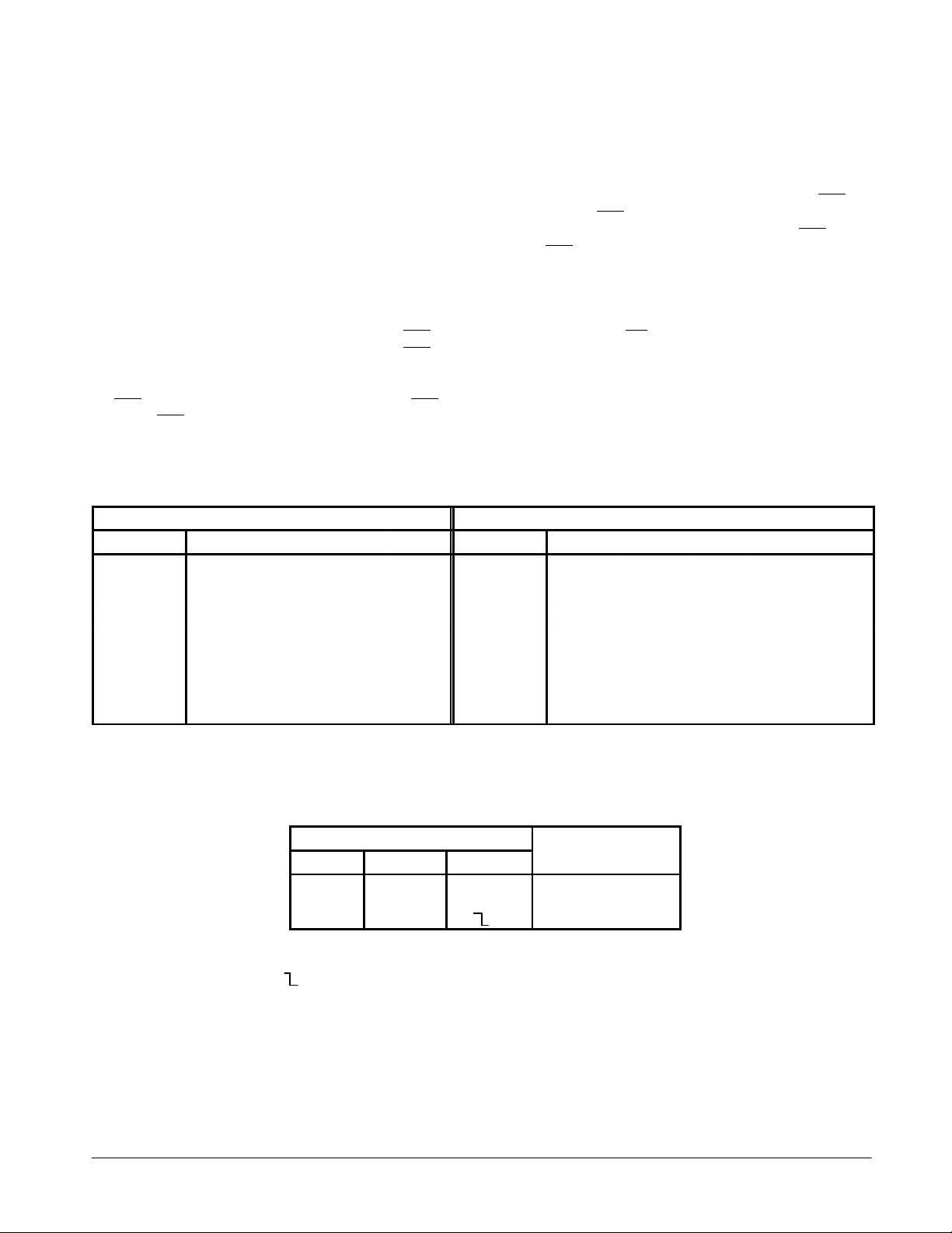
Figure 2. LS196 COUNT SEQUENCES
DECADE (NOTE 1) BI-QUINARY (NOTE 2)
COUNT Q
0 L L L L 0 L L L L
1 L LLH 1 L LL H
2 LLHL 2 L LH L
3 LLHH 3 L LH H
4 LHLL 4 L HL L
5 LHLH 5 H LL L
6 LHHL 6 H LL H
7 LHHH 7 H LH L
8 HLLL 8 H LH H
9 HL L H 9 H HL L
NOTES:
1. Signal applied to CP0, Q0 connected to CP1.
2. Signal applied to CP1, Q3 connected to CP0.
3
Q
2
Q
1
Q
0
significant output.
The LS196 Decade Counter can be connected up to operate in two different count sequences, as indicated in the tables
of Figure 2. With the input frequency connected to CP
with Q0 driving CP
, the circuit counts in the BCD (8, 4, 2, 1)
1
sequence. With the input frequency connected to CP
driving CP
, Q0 becomes the low frequency output and has a
0
50% duty cycle waveform. Note that the maximum counting
rate is reduced in the latter (bi-quinary) configuration because
of the interstage gating delay within the divide-by-five section.
The LS196 and LS197 have an asynchronous active LOW
Master Reset input (MR
) which overrides all other inputs and
forces all outputs LOW. The counters are also asynchronously
presettable. A LOW on the Parallel Load input (PL) overrides
0
the clock inputs and loads the data from Parallel Data (P0–P3)
inputs into the flip-flops. While PL is LOW, the counters act as
transparent latches and any change in the Pn inputs will be reflected in the outputs.
COUNT Q
0
Q
3
Q
2
Q
1
1
and
0
and Q
3
MODE SELECT TABLE
INPUTS
MR PL CP
L X X Reset (Clear)
H L X Parallel Load
H H Count
H = HIGH Voltage Level
L = LOW Voltage Level
X = Don’t Care
= HIGH to Low Clock Transition
FAST AND LS TTL DATA
5-3
Page 4
SN54/74LS196 • SN54/74LS197
VILI
LOW Volt
V
pg
VOHOutput HIGH Volt
CC
,
OH
,
IN IH
VOLOutput LOW Volt
V
V
V
I
IH
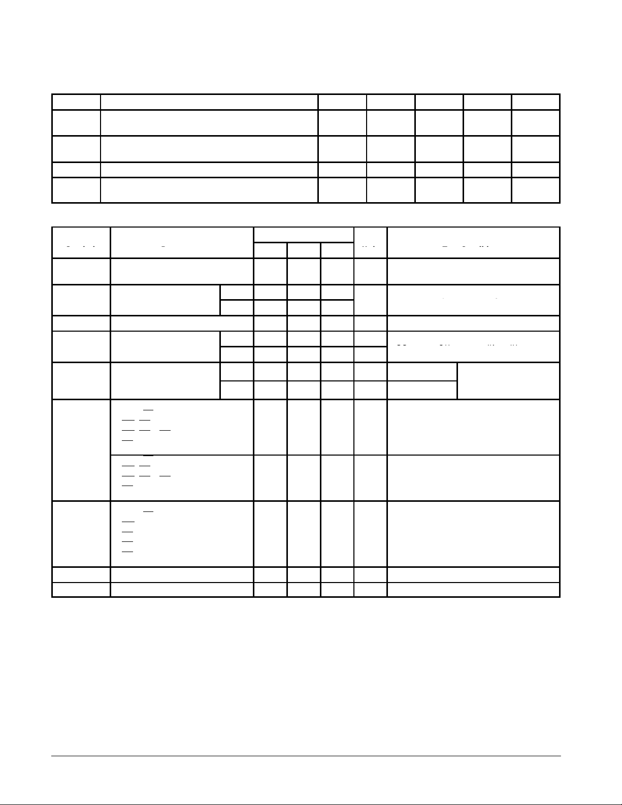
GUARANTEED OPERATING RANGES
Symbol Parameter Min Typ Max Unit
V
CC
T
A
I
OH
I
OL
DC CHARACTERISTICS OVER OPERATING TEMPERATURE RANGE (unless otherwise specified)
Symbol Parameter
V
IH
V
IK
I
IH
I
IL
I
OS
I
CC
Note 1: Not more than one output should be shorted at a time, nor for more than 1 second.
Supply Voltage 54
Operating Ambient Temperature Range 54
Output Current — High 54, 74 –0.4 mA
Output Current — Low 54
Limits
Min Typ Max
Input HIGH Voltage 2.0 V
nput
Input Clamp Diode Voltage –0.65 –1.5 V VCC = MIN, IIN = –18 mA
Input HIGH Current
Data, PL
MR, CP0 (LS196)
MR, CP
CP1 (LS196)
Data, PL
MR, CP0 (LS196)
MR
, CP
CP1 (LS196)
Input LOW Current
Data, PL
MR
CP
0
CP1 (LS196)
CP
(LS197)
1
Short Circuit Current (Note 1) –20 –100 mA VCC = MAX
Power Supply Current 27 mA VCC = MAX
age
age
age
, CP1 (LS197)
0
, CP1 (LS197)
0
54 0.7
74 0.8
54 2.5 3.5 V
74 2.7 3.5 V
54, 74 0.25 0.4 V IOL = 4.0 mA
74 0.35 0.5 V IOL = 8.0 mA
74
74
74
20
40
40
80
0.1
0.2
0.2
0.4
–0.4
–0.8
–2.4
–2.8
–1.3
4.5
4.75
–55
0
Unit Test Conditions
Guaranteed Input HIGH Voltage for
All Inputs
Guaranteed Input LOW Voltage for
All Inputs
VCC = MIN, IOH = MAX, VIN = V
or VIL per Truth Table
µA VCC = MAX, VIN = 2.7 V
mA VCC = MAX, VIN = 7.0 V
mA VCC = MAX, VIN = 0.4 V
5.0
5.0
25
25
5.5
5.25
125
70
4.0
8.0
VCC = VCC MIN,
=
IN
IL
per Truth Table
or
IH
IH
V
°C
mA
FAST AND LS TTL DATA
5-4
Page 5
SN54/74LS196 • SN54/74LS197
CC
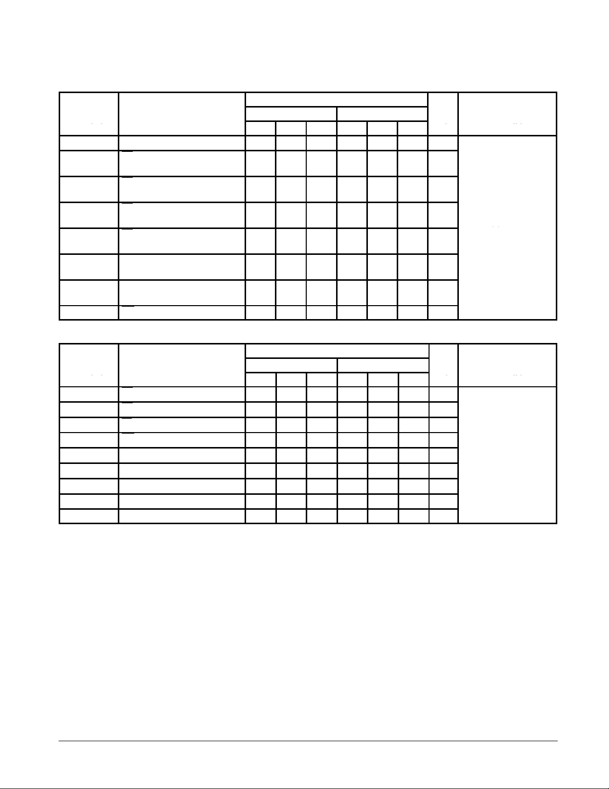
AC CHARACTERISTICS (T
Symbol Parameter
f
MAX
t
PLH
t
PHL
t
PLH
t
PHL
t
PLH
t
PHL
t
PLH
t
PHL
t
PLH
t
PHL
t
PLH
t
PHL
t
PHL
Maximum Clock Frequency 30 40 30 40 MHz
CP0 Input to
Q0 Output
CP
Input to
1
Q1 Output
CP1 Input to
Q2 Output
CP
Input to
1
Q3 Output
Data to Output
PL Input to
Any Output
MR Input to Any Output 34 51 34 51 ns
= 25°C)
A
AC SETUP REQUIREMENTS (T
Symbol Parameter
t
t
t
t
t
t
t
t
t
W
W
W
W
s
s
h
h
rec
CP0 Pulse Width 20 20 ns
CP1 Pulse Width 30 30 ns
PL Pulse Width 20 20 ns
MR Pulse Width 15 15 ns
Data Input Setup Time — HIGH 10 10 ns
Data Input Setup Time — LOW 15 15 ns
Data Hold Time — HIGH 10 10 ns
Data Hold Time — LOW 10 10 ns
Recovery Time 30 30 ns
= 25°C)
A
Limits
LS196 LS197
Min Typ Max Min Typ Max
8.0
13
16
22
38
41
12
30
20
29
27
30
LS196 LS197
Min Typ Max Min Typ Max
15
20
24
33
57
62
18
45
30
44
41
45
Limits
8.0
14
12
23
34
42
55
63
18
29
26
30
15
21
19
35
51
63
78
95
27
44
39
45
Unit T est Conditions
ns
ns
ns
ns
ns
ns
Unit Test Conditions
VCC = 5.0 V
CL = 15 pF
VCC = 5.0 V
DEFINITIONS OF TERMS
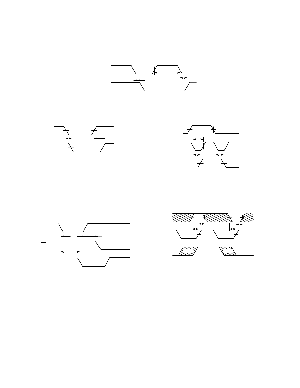
SETUP TIME (ts) — is defined as the minimum time required
for the correct logic level to be present at the logic input prior to
the clock transition from HIGH to LOW in order to be recognized and transferred to the outputs.
HOLD TIME (th) — is defined as the minimum time following
the clock transition from HIGH to LOW that the logic level must
be maintained at the input in order to ensure continued recog-
nition. A negative HOLD TIME indicates that the correct logic
level may be released prior to the clock transition from HIGH to
LOW and still be recognized.
RECOVERY TIME (t
required between the end of the reset pulse and the clock
transition from HIGH to LOW in order to recognize and transfer
LOW Data to the Q outputs.
FAST AND LS TTL DATA
5-5
) — is defined as the minimum time
rec
Page 6
SN54/74LS196 • SN54/74LS197
AC WAVEFORMS
P
n
t
PHL
Q
n
NOTE: PL = LOW
CP 1.3 V 1.3 V
t
PHL
Q
1.3 V 1.3 V
t
W(H)
t
PLH
Figure 1
1.3 V 1.3 V
1.3 V
t
PLH
P
n
1.3 VPL
t
PLH
Q
n
1.3 V
Figure 2 Figure 3
t
W
t
PHL
PL
OR MR
CP
Pn*
1.3 V
t
W
1.3 V
t
PHL
Q
1.3 V
t
rec
PL
Qn*
* The shaded areas indicate when the input is permitted
* to change for predictable output performance
1.3 V 1.3 V
t
t
s(H)
Q = P Q = P
h(H)
t
s(L)
t
h(L)
1.3 V1.3 V
Figure 4 Figure 5
FAST AND LS TTL DATA
5-6
 Loading...