

Page 1
UNIVERSAL 4-BIT
SHIFT REGISTER
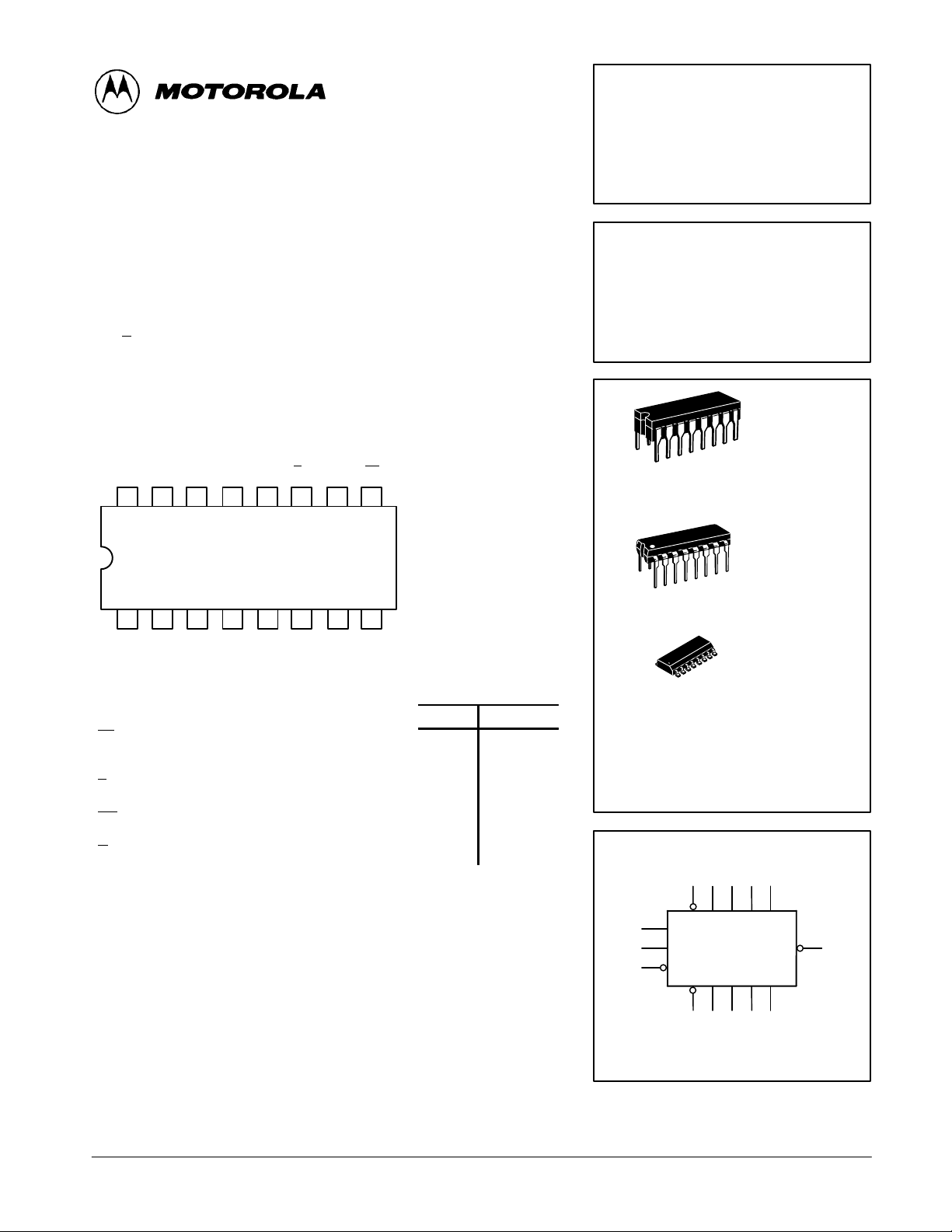
The SN54/74LS195A is a high speed 4-Bit Shift Register offering typical
shift frequencies of 39 MHz. It is useful for a wide variety of register and
counting applications. It utilizes the Schottky diode clamped process to
achieve high speeds and is fully compatible with all Motorola TTL products.
• Typical Shift Right Frequency of 39 MHz
• Asynchronous Master Reset
• J, K Inputs to First Stage
• Fully Synchronous Serial or Parallel Data Transfers
• Input Clamp Diodes Limit High Speed Termination Effects
CONNECTION DIAGRAM DIP (TOP VIEW)
Q0Q1Q2Q
V
CC
16 15
3
14 13 12 11 10 9
CPQ
3
PE
SN54/74LS195A
UNIVERSAL 4-BIT
SHIFT REGISTER
LOW POWER SCHOTTKY
J SUFFIX
CERAMIC
16
1
CASE 620-09
NOTE:
The Flatpak version
has the same pinouts
(Connection Diagram) as
the Dual In-Line Package.
123456
JKP
MR
PIN NAMES LOADING (Note a)
PE Parallel Enable (Active LOW) Input 0.5 U.L. 0.25 U.L.
P0 – P
J First Stage J (Active HIGH) Input 0.5 U.L. 0.25 U.L.
K First Stage K (Active LOW) Input 0.5 U.L. 0.25 U.L.
CP Clock (Active HIGH Going Edge) Input 0.5 U.L. 0.25 U.L.
MR Master Reset (Active LOW) Input 0.5 U.L. 0.25 U.L.
Q0 – Q
Q
3
NOTES:
a. 1 TTL Unit Load (U.L.) = 40 µA HIGH/1.6 mA LOW.
b. The Output LOW drive factor is 2.5 U.L. for Military (54) and 5 U.L. for Commercial (74)
b. T emperature Ranges.
Parallel Data Inputs 0.5 U.L. 0.25 U.L.
3
Parallel Outputs (Note b) 10 U.L. 5 (2.5) U.L.
3
Complementary Last Stage Output (Note b) 10 U.L. 5 (2.5) U.L.
P
0
P
1
2
7
P
GND
3
8
HIGH
LOW
N SUFFIX
16
1
16
1
CASE 648-08
D SUFFIX
CASE 751B-03
ORDERING INFORMATION
SN54LSXXXJ Ceramic
SN74LSXXXN Plastic
SN74LSXXXD SOIC
LOGIC SYMBOL
456 7
9
P0P1P2P
J
CP
K
PE
MR
Q0Q1Q2Q
2
10
3
PLASTIC
SOIC
3
Q
3
3
11
FAST AND LS TTL DAT A
5-1
121314151
VCC = PIN 16
GND = PIN 8
Page 2
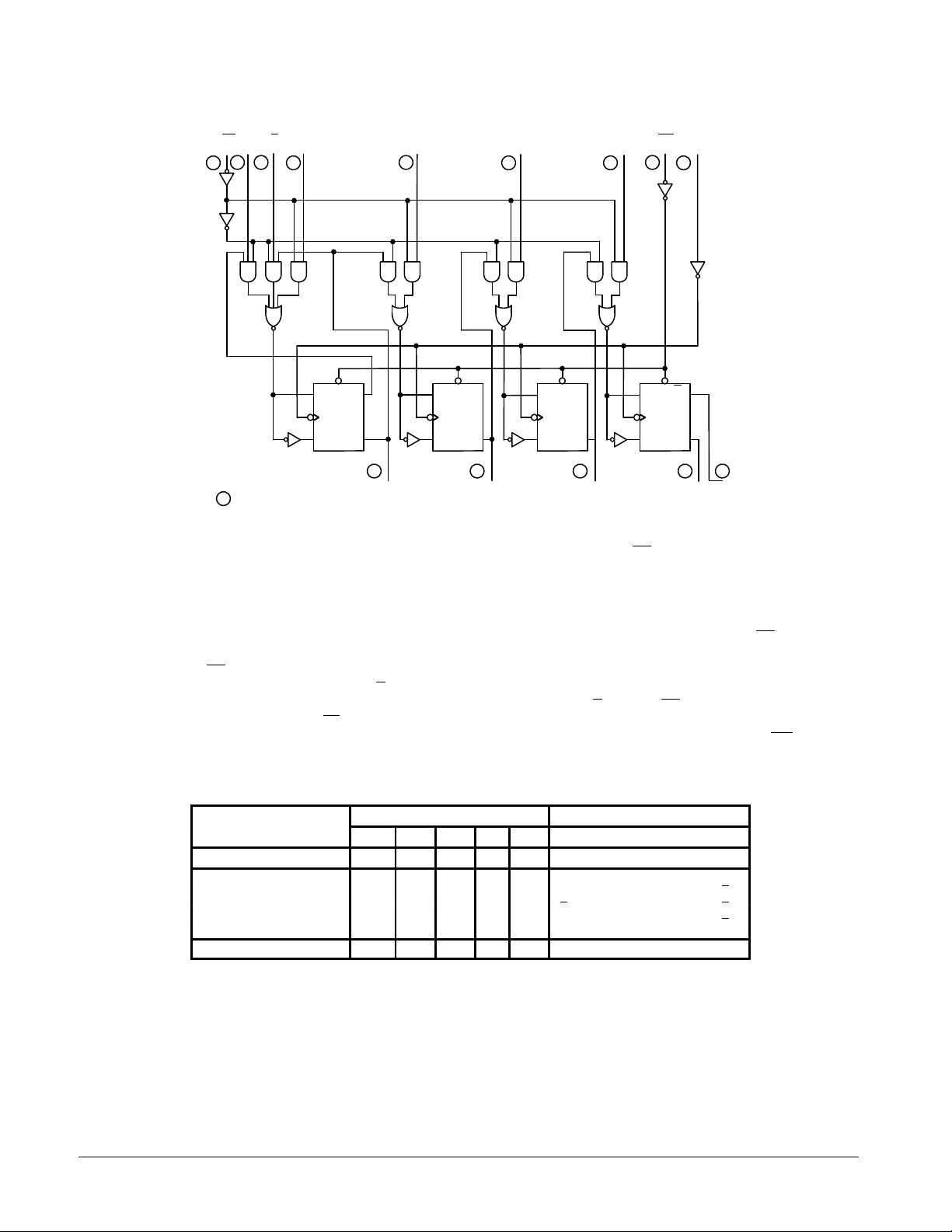
LOGIC DIAGRAM
OPERATING MODES
JP
0
SN54/74LS195A
P
1
P
2
P
3
12 6734 59
CPPE K MR
10
C
Q
VCC = PIN 16
GND = PIN 8
= PIN NUMBERS
R
S
CP
D
0
Q
0
Q
0
R
S
FUNCTIONAL DESCRIPTION
The Logic Diagram and Truth Table indicate the functional
characteristics of the LS195A 4-Bit Shift Register. The device
is useful in a wide variety of shifting, counting and storage
applications. It performs serial, parallel, serial to parallel, or
parallel to serial data transfers at very high speeds.
The LS195A has two primary modes of operation, shift right
(Q0 → Q1) and parallel load which are controlled by the state of
the Parallel Enable (PE
serial data enters the first flip-flop Q0 via the J and K
) input. When the PE input is HIGH,
inputs and
is shifted one bit in the direction Q0 → Q1 → Q2 → Q3 following
each LOW to HIGH clock transition. The JK
inputs provide the
flexibility of the JK type input for special applications, and the
simple D type input for general applications by tying the two
MODE SELECT — TRUTH TABLE
INPUTS OUTPUTS
MR PE J K P
Asynchronous Reset L X X X X L L L L H
Shift, Set First Stage H h h h X H q
Shift, Reset First H h I I X L q
Shift, Toggle First Stage H h h I X q
Shift, Retain First Stage H h I h X q
Parallel Load H I X X p
L = LOW voltage levels
H = HIGH voltage levels
X = Don’t Care
I = LOW voltage level one set-up time prior to the LOW to HIGH clock transition.
h = HIGH voltage level one set-up time prior to the LOW to HIGH clock transition.
pn (qn) = Lower case letters indicate the state of the referenced input (or output) one set-up time prior to the LOW to
HIGH clock transition.
C
D
CP
Q
0
14
Q
1
pins together. When the PE
R
S
CP
C
D
Q
2
1315
Q
2
C
Q
R
D
3
CP
S
Q
3
1112
Q
Q
3
3
input is LOW, the LS195A appears
as four common clocked D flip-flops. The data on the parallel
inputs P0, P1, P2, P3 is transferred to the respective Q0, Q1,
Q2, Q3 outputs following the LOW to HIGH clock transition.
Shift left operations (Q3 →Q2) can be achieved by tying the Q
Outputs to the P
inputs and holding the PE
n–1
All serial and parallel data transfers are synchronous,
occurring after each LOW to HIGH clock transition. Since the
LS195A utilizes edge-triggering, there is no restriction on the
activity of the J, K
, Pn and PE inputs for logic operation —
except for the set-up and release time requirements.
A LOW on the asynchronous Master Reset (MR
all Q outputs LOW, independent of any other input condition.
n
n
Q0Q
0
0
p
0
Q
1
0
0
q
0
q
0
p
1
Q3Q
2
q
1
q
1
q
1
q
1
p
2
q2q
q2q
q2q
q2q
p3p
3
2
2
2
2
3
input LOW.
n
) input sets
FAST AND LS TTL DATA
5-2
Page 3
SN54/74LS195A
VILI
LOW Volt
V
pg
VOHOutput HIGH Volt
CC
,
OH
,
IN IH
VOLOutput LOW Volt
V
V
V
IIHI
HIGH C
t
C
L
pF
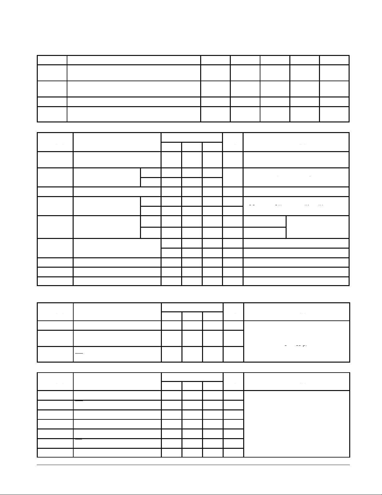
GUARANTEED OPERATING RANGES
Symbol Parameter Min Typ Max Unit
V
CC
T
A
I
OH
I
OL
DC CHARACTERISTICS OVER OPERATING TEMPERATURE RANGE (unless otherwise specified)
Symbol Parameter
V
IH
V
IK
I
IL
I
OS
I
CC
Note 1: Not more than one output should be shorted at a time, nor for more than 1 second.
AC CHARACTERISTICS (T
Symbol Parameter
f
MAX
t
PLH
t
PHL
t
PHL
Supply Voltage 54
Operating Ambient Temperature Range 54
Output Current — High 54, 74 –0.4 mA
Output Current — Low 54
Limits
Min Typ Max
Input HIGH Voltage 2.0 V
nput
Input Clamp Diode Voltage –0.65 –1.5 V VCC = MIN, IIN = –18 mA
nput
Input LOW Current –0.4 mA VCC = MAX, VIN = 0.4 V
Short Circuit Current (Note 1) –20 –100 mA VCC = MAX
Power Supply Current 21 mA VCC = MAX
Maximum Clock Frequency 30 39 MHz
Propagation Delay,
Clock to Output
Propagation Delay,
MR to Output
age
age
age
urren
= 25°C)
A
54 0.7
74 0.8
54 2.5 3.5 V
74 2.7 3.5 V
54, 74 0.25 0.4 V IOL = 4.0 mA
74 0.35 0.5 V IOL = 8.0 mA
Limits
Min Typ Max
14
17
19 30 ns
74
74
74
20 µA VCC = MAX, VIN = 2.7 V
0.1 mA VCC = MAX, VIN = 7.0 V
22
26
4.5
4.75
–55
0
Unit Test Conditions
Guaranteed Input HIGH Voltage for
All Inputs
Guaranteed Input LOW Voltage for
All Inputs
VCC = MIN, IOH = MAX, VIN = V
or VIL per Truth Table
Unit Test Conditions
ns
5.0
5.0
25
25
VCC = 5.0 V
C
5.5
5.25
125
70
4.0
8.0
VCC = VCC MIN,
=
IN
IL
per Truth Table
= 15 pF
= 15
or
IH
IH
V
°C
mA
AC SETUP REQUIREMENTS (T
Symbol Parameter
t
t
t
t
t
t
t
W
W
s
s
rec
rel
h
CP Clock Pulse Width 16 ns
MR Pulse Width 12 ns
PE Setup Time 25 ns
Data Setup Time 15 ns
Recovery Time 25 ns
PE Release Time 10 ns
Data Hold Time 0 ns
= 25°C)
A
Limits
Min Typ Max
FAST AND LS TTL DATA
5-3
Unit Test Conditions
VCC = 5.0 V
Page 4
SN54/74LS195A
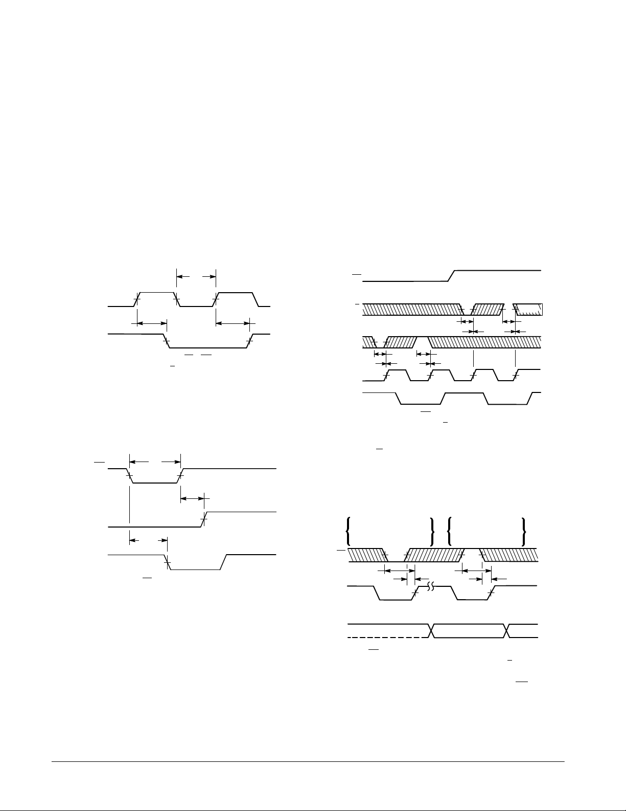
DEFINITIONS OF TERMS
SETUP TIME(ts) —is defined as the minimum time required
for the correct logic level to be present at the logic input prior
to the clock transition from LOW to HIGH in order to be
recognized and transferred to the outputs.
HOLD TIME (th) — is defined as the minimum time following
the clock transition from LOW to HIGH that the logic level must
be maintained at the input in order to ensure continued
AC WAVEFORMS
The shaded areas indicate when the input is permitted to change for predictable output performance.
t
W
recognition. A negative HOLD TIME indicates that the correct
logic level may be released prior to the clock transition from
LOW to HIGH and still be recognized.
RECOVERY TIME (t
) — is defined as the minimum time
rec
required between the end of the reset pulse and the clock
transition from LOW to HIGH in order to recognize and transfer
HIGH Data to the Q outputs.
PE
CLOCK
OUTPUT
1.3 V 1.3 V
t
PHL
1.3 V 1.3 V
CONDITIONS: J = PE
K
= L
= MR = H
Figure 1. Clock to Output Delays and
Clock Pulse Width
t
MR
CLOCK
OUTPUT
CONDITIONS: PE = L
PO = P1 = P2 = P3 = H
1.3 V
t
PHL
W
1.3 V
t
rec
1.3 V
1.3 V
t
PLH
J & K
P0 P1 P2 P
th(L) = 0
CLOCK
OUTPUT*
3
ts(L)
CONDITIONS: MR
*J AND K
ts(L)
th(L) = 0 th(H) = 0
ts(H)
th(H) = 0
1.3 V
= H
SET–UP TIME AFFECTS Q0 ONLY
1.3 V
ts(H)
1.3 V
Figure 3. Setup (ts) and Hold (th) Time for Serial Data
(J & K
) and Parallel Data (P0, P1, P2, P3)
PE
CLOCK
LOAD PARALLEL DATA LOAD SERIAL DATA
1.3 V
ts(L) ts(H)
t
rel
1.3 V
SHIFT RIGHT
1.3 V
t
rel
1.3 V
Figure 2. Master Reset Pulse Width, Master Reset
to Output Delay and Master Reset to Clock
Recovery Time
FAST AND LS TTL DATA
OUTPUT
CONDITIONS: MR = H
*Q0 STATE WILL BE DETERMINED BY J AND K
Qn = P
n
Figure 4. Setup (ts) and Hold (th) Time for PE
5-4
Qn* = Q
n–1
INPUTS .
Input
 Loading...