

Page 1
4-BIT BIDIRECTIONAL
UNIVERSAL SHIFT REGISTER
The SN54 /74LS194A is a High Speed 4-Bit Bidirectional Universal Shift
Register. As a high speed multifunctional sequential building block, it is useful
in a wide variety of applications. It may be used in serial-serial, shift left, shift
right, serial-parallel, parallel-serial, and parallel-parallel data register transfers. The LS194A is similar in operation to the LS195A Universal Shift
Register, with added features of shift left without external connections and
hold (do nothing) modes of operation. It utilizes the Schottky diode clamped
process to achieve high speeds and is fully compatible with all Motorola TTL
families.
• Typical Shift Frequency of 36 MHz
• Asynchronous Master Reset
• Hold (Do Nothing) Mode
• Fully Synchronous Serial or Parallel Data Transfers
• Input Clamp Diodes Limit High Speed Termination Effects
SN54/74LS194A
4-BIT BIDIRECTIONAL
UNIVERSAL SHIFT REGISTER
LOW POWER SCHOTTKY
J SUFFIX
CERAMIC
16
1
CASE 620-09
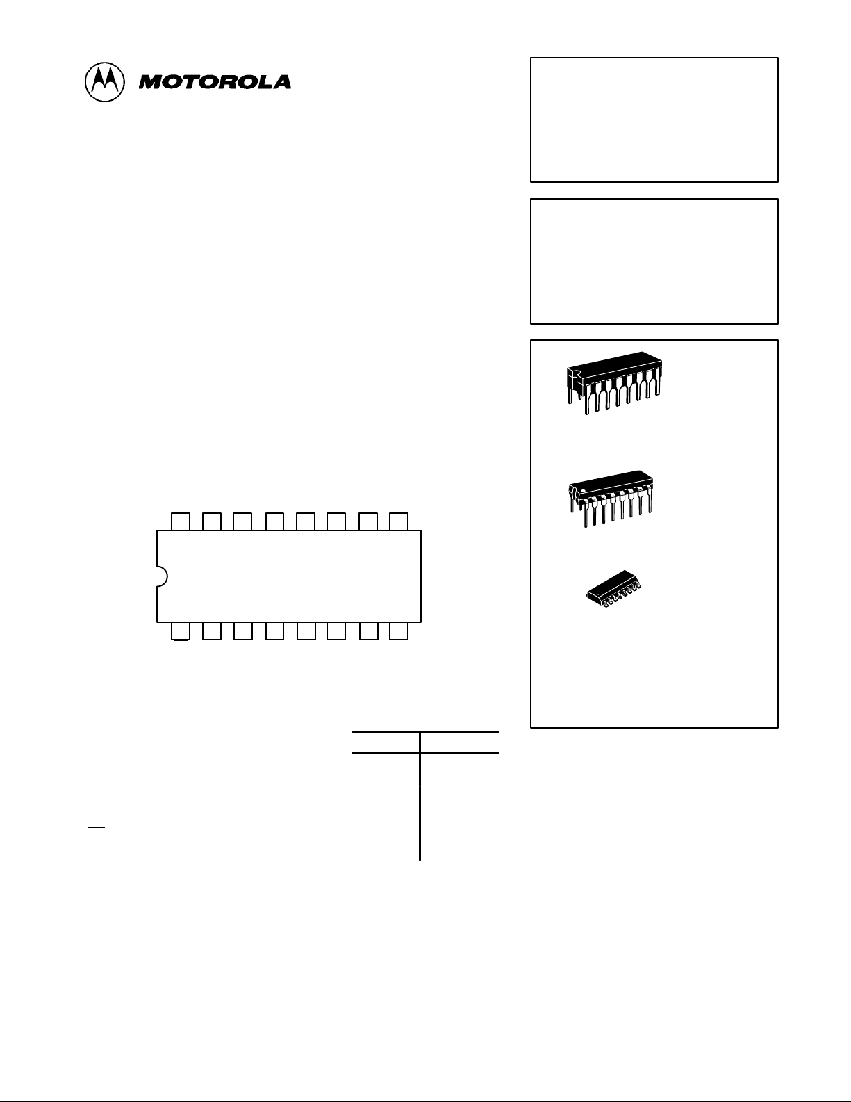
CONNECTION DIAGRAM DIP (TOP VIEW)
Q0Q1Q2Q
V
CC
16 15
123456
MR
PIN NAMES LOADING (Note a)
S0, S
1
P0–P
D
SR
D
SL
CP Clock (Active HIGH Going Edge) Input 0.5 U.L. 0.25 U.L.
MR Master Reset (Active LOW) Input 0.5 U.L. 0.25 U.L.
Q0–Q
NOTES:
a. 1 TTL Unit Load (U.L.) = 40 µA HIGH/1.6 mA LOW.
b. The Output LOW drive factor is 2.5 U.L. for Military (54) and 5 U.L. for Commercial (74)
b. T emperature Ranges.
Mode Control Inputs 0.5 U.L. 0.25 U.L.
Parallel Data Inputs 0.5 U.L. 0.25 U.L.
3
Serial (Shift Right) Data Input 0.5 U.L. 0.25 U.L.
Serial (Shift Left) Data Input 0.5 U.L. 0.25 U.L.
Parallel Outputs (Note b) 10 U.L. 5 (2.5) U.L.
3
14 13 12 11 10 9
DSRP0P1P2P3DSLGND
3
S
CP S
1
7
HIGH
0
8
LOW
N SUFFIX
16
1
16
1
CASE 648-08
D SUFFIX
CASE 751B-03
ORDERING INFORMATION
SN54LSXXXJ Ceramic
SN74LSXXXN Plastic
SN74LSXXXD SOIC
PLASTIC
SOIC
FAST AND LS TTL DAT A
5-1
Page 2
SN54/74LS194A
OPERATING MODE
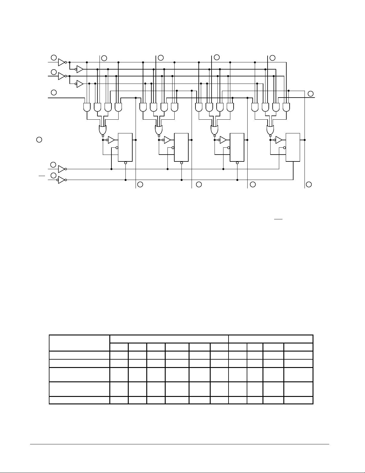
LOGIC DIAGRAM
10
S
1
9
S
0
2
D
SR
P
0
3
P
1
4
VCC = PIN 16
GND = PIN 8
= PIN NUMBERS
11
CP
1
MR
SQ
0
CP
R
CLEAR
Q
0
FUNCTIONAL DESCRIPTION
The Logic Diagram and Truth Table indicate the functional
characteristics of the LS194A 4-Bit Bidirectional Shift Register. The LS194A is similar in operation to the Motorola LS195A
Universal Shift Register when used in serial or parallel data
register transfers. Some of the common features of the two
devices are described below:
All data and mode control inputs are edge-triggered,
responding only to the LOW to HIGH transition of the Clock
(CP). The only timing restriction, therefore, is that the mode
control and selected data inputs must be stable one set-up
time prior to the positive transition of the clock pulse.
The register is fully synchronous, with all operations taking
place in less than 15 ns (typical) making the device especially
useful for implementing very high speed CPUs, or the memory
buffer registers.
The four parallel data inputs (P0, P1, P2, P3) are D-type
inputs. When both S0 and S1 are HIGH, the data appearing on
P0, P1, P2, and P3 inputs is transferred to the Q0, Q1, Q2, and
MODE SELECT — TRUTH TABLE
INPUTS OUTPUTS
MR S
Reset L X X X X X L L L L
Hold H I I X X X q
Shift Left H h I X I X q
H h I X h X q
Shift Right H I h I X X L q
H I h h X X H q
Parallel Load H h h X X P
L = LOW Voltage Level
H = HIGH Voltage Level
X = Don’t Care
I = LOW voltage level one set-up time prior to the LOW to HIGH clock transition
h = HIGH voltage level one set-up time prior to the LOW to HIGH clock transition
pn (qn) = Lower case letters indicate the state of the referenced input (or output) one set-up time prior to the LOW to HIGH clock transition.
S
1
0
SQ
1
CP
R
CLEAR
Q
P
2
5
SQ
2
CP
R
CLEAR
14
1
Q
P
3
6
SQ
CP
R
CLEAR
1315
2
Q3 outputs respectively following the next LOW to HIGH
transition of the clock.
The asynchronous Master Reset (MR
), when LOW, over-
rides all other input conditions and forces the Q outputs LOW.
Special logic features of the LS194A design which increase
the range of application are described below:
Two mode control inputs (S0, S1) determine the synchronous operation of the device. As shown in the Mode Selection
Table, data can be entered and shifted from left to right (shift
right, Q0 →Q1, etc.) or right to left (shift left, Q3 →Q2, etc.), or
parallel data can be entered loading all four bits of the register
simultaneously . When both S0 and S1,are LOW, the existing
data is retained in a “do nothing” mode without restricting the
HIGH to LOW clock transition.
D-type serial data inputs (DSR, DSL) are provided on both
the first and last stages to allow multistage shift right or shift left
data transfers without interfering with parallel load operation.
D
SR
D
SL
P
Q
n
Q
0
0
1
1
P
n
P
0
Q
1
q
1
q
2
q
2
0
0
1
2
q
2
q
3
q
3
q
1
q
1
P
2
Q
q
H
q
q
P
3
3
3
L
2
2
3
7
D
SL
12
Q
3
FAST AND LS TTL DATA
5-2
Page 3
SN54/74LS194A
VILI
LOW Volt
V
pg
VOHOutput HIGH Volt
CC
,
OH
,
IN IH
VOLOutput LOW Volt
V
V
V
IIHI
HIGH C
t
C
L
pF
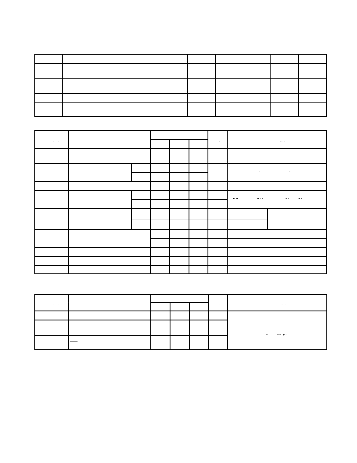
GUARANTEED OPERATING RANGES
Symbol Parameter Min Typ Max Unit
V
CC
T
A
I
OH
I
OL
DC CHARACTERISTICS OVER OPERATING TEMPERATURE RANGE (unless otherwise specified)
Symbol Parameter
V
IH
V
IK
I
IL
I
OS
I
CC
Note 1: Not more than one output should be shorted at a time, nor for more than 1 second.
Supply Voltage 54
Operating Ambient Temperature Range 54
Output Current — High 54, 74 –0.4 mA
Output Current — Low 54
Limits
Min Typ Max
Input HIGH Voltage 2.0 V
nput
Input Clamp Diode Voltage –0.65 –1.5 V VCC = MIN, IIN = –18 mA
nput
Input LOW Current –0.4 mA VCC = MAX, VIN = 0.4 V
Short Circuit Current (Note 1) –20 –100 mA VCC = MAX
Power Supply Current 23 mA VCC = MAX
age
age
age
urren
54 0.7
74 0.8
54 2.5 3.5 V
74 2.7 3.5 V
54, 74 0.25 0.4 V IOL = 4.0 mA
74 0.35 0.5 V IOL = 8.0 mA
74
74
74
20 µA VCC = MAX, VIN = 2.7 V
0.1 mA VCC = MAX, VIN = 7.0 V
4.5
4.75
–55
0
Unit Test Conditions
Guaranteed Input HIGH Voltage for
All Inputs
Guaranteed Input LOW Voltage for
All Inputs
VCC = MIN, IOH = MAX, VIN = V
or VIL per Truth Table
5.0
5.0
25
25
5.5
5.25
125
70
4.0
8.0
VCC = VCC MIN,
=
IN
IL
per Truth Table
or
IH
IH
V
°C
mA
AC CHARACTERISTICS (T
Symbol Parameter
f
MAX
t
PLH
t
PHL
t
PHL
Maximum Clock Frequency 25 36 MHz
Propagation Delay,
Clock to Output
Propagation Delay,
MR to Output
A
= 25°C)
Limits
Min Typ Max
14
17
19 30 ns
22
26
FAST AND LS TTL DATA
5-3
Unit Test Conditions
ns
VCC = 5.0 V
C
= 15 pF
= 15
Page 4
SN54/74LS194A
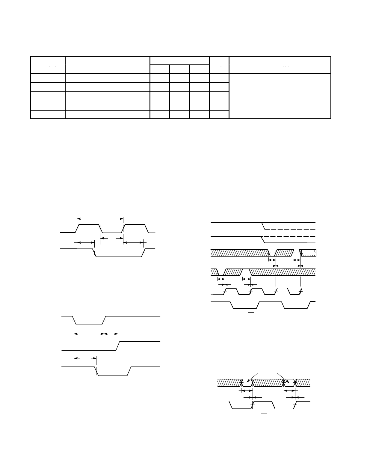
AC SETUP REQUIREMENTS (T
Symbol Parameter
t
t
t
t
t
W
s
s
h
rec
Clock or MR Pulse Width 20 ns
Mode Control Setup Time 30 ns
Data Setup Time 20 ns
Hold time, Any Input 0 ns
Recovery Time 25 ns
= 25°C)
A
Min Typ Max
DEFINITIONS OF TERMS
SETUP TIME(ts) —is defined as the minimum time required
for the correct logic level to be present at the logic input prior
to the clock transition from LOW to HIGH in order to be
recognized and transferred to the outputs.
HOLD TIME (th) — is defined as the minimum time following
the clock transition from LOW to HIGH that the logic level must
be maintained at the input in order to ensure continued
AC WAVEFORMS
The shaded areas indicate when the input is permitted to change for predictable output performance.
1/fmax
CLOCK
OUTPUT
OTHER CONDITIONS: S1 = L, MR = H, S0 = H
1.3 V 1.3 V
t
PHL
1.3 V
t
W
t
PLH
1.3 V
Figure 1. Clock to Output Delays Clock Pulse
Width and f
max
Limits
Unit Test Conditions
VCC = 5.0 V
recognition. A negative HOLD TIME indicates that the correct
logic level may be released prior to the clock transition from
LOW to HIGH and still be recognized.
RECOVERY TIME (t
) — is defined as the minimum time
rec
required between the end of the reset pulse and the clock
transition from LOW to HIGH in order to recognize and transfer
HIGH Data to the Q outputs.
S
DSR D
P0 P1 P2 P
CLOCK
OUTPUT*
0
S
1
SL
3
th(L) = 0
ts(L)
1.3 V
(––– IS SHIFT LEFT)
ts(L)
th(L) = 0 th(H) = 0
ts(H)
th(H) = 0
1.3 V
1.3 V
ts(H)
MR
CLOCK
OUTPUT
OTHER CONDITIONS: S0, S1 = H
OTHER CONDITIONS: PO = P1 = P2 = P3 = H
1.3 V
t
PHL
t
W
1.3 V
t
rec
1.3 V
Figure 2. Master Reset Pulse Width, Master Reset
to Output Delay and Master Reset to Clock
Recovery Time
FAST AND LS TTL DATA
OTHER CONDITIONS: MR
OTHER CONDITIONS: *DSR SET-UP TIME AFFECTS Q0 ONLY
OTHER CONDITIONS: DSL SET-UP TIME AFFECTS Q3 ONLY
= H
Figure 3. Setup (ts) and Hold (th) Time for Serial Data
(DSR, DSL) and Parallel Data (P0, P1, P2, P3)
(STABLE TIME)
S0 S
1
CLOCK
t
s
th = 0 th = 0
1.3 V
OTHER CONDITIONS: MR
= H
Figure 4. Setup (ts) and Hold (th) Time for S Input
5-4
t
s
1.3 V
1.3 V
 Loading...