

Page 1
4-BIT ARITHMETIC
LOGIC UNIT
The SN54/74LS181 is a 4-bit Arithmetic Logic Unit (ALU) which can
perform all the possible 16 logic, operations on two variables and a variety of
arithmetic operations.
• Provides 16 Arithmetic Operations Add, Subtract, Compare, Double,
Plus Twelve Other Arithmetic Operations
• Provides all 16 Logic Operations of Two Variables Exclusive — OR,
Compare, AND, NAND, OR, NOR, Plus Ten other Logic Operations
• Full Lookahead for High Speed Arithmetic Operation on Long Words
• Input Clamp Diodes
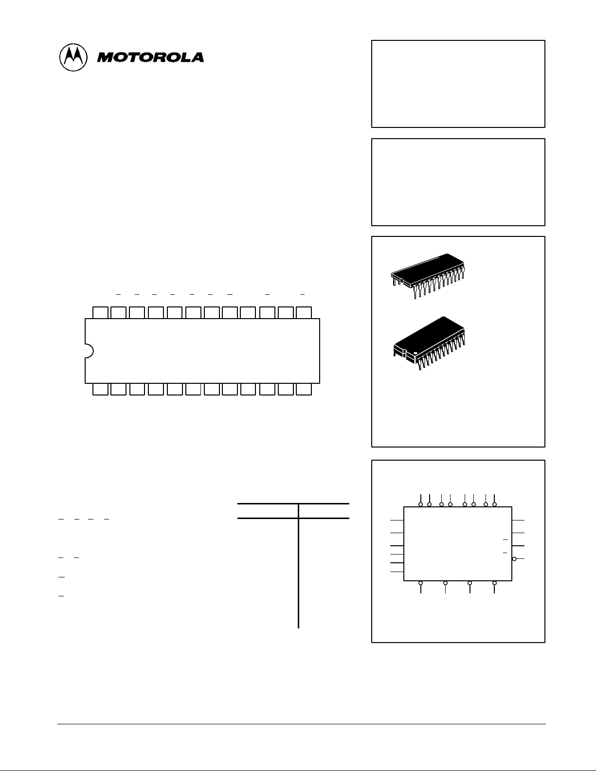
CONNECTION DIAGRAM DIP (TOP VIEW)
A
V
CC
1B1A2B2
24 23
1234 56
B
0
22 21 20 19 18 17
A0S3S2S1S0CnM
NOTE:
The Flatpak version
has the same pinouts
(Connection Diagram) as
the Dual In-Line Package.
A
3
B
3
7
C
G
n+4
16 15 14 13
8
9101112
F
0F1F2
F
A=BP
3
GND
SN54/74LS181
4-BIT ARITHMETIC
LOGIC UNIT
LOW POWER SCHOTTKY
J SUFFIX
CERAMIC
24
1
24
1
ORDERING INFORMATION
SN54LSXXXJ Ceramic
SN74LSXXXN Plastic
CASE 623-05
N SUFFIX
PLASTIC
CASE 649-03
PIN NAMES LOADING (Note a)
HIGH
A0–A3, B0–B
S0–S
3
M
C
n
F
0–F3
A = B
G
P
C
n+4
NOTES:
a. 1 TTL Unit Load (U.L.) = 40 µA HIGH/1.6 mA LOW.
b. The Output LOW drive factor is 2.5 U.L. for Military (54) and 5 U.L. for Commercial (74)
b. T emperature Ranges.
Operand (Active LOW) Inputs
3
Function — Select Inputs
Mode Control Input
Carry Input
Function (Active LOW) Outputs
Comparator Output
Carry Generator (Active LOW)
Output
Carry Propagate (Active LOW)
Output
Carry Output
1.5 U.L.
2.0 U.L.
0.5 U.L.
2.5 U.L.
10 U.L.
Open Collector
10 U.L.
10 U.L.
10 U.L.
LOW
0.75 U.L.
0.25 U.L.
1.25 U.L.
5 (2.5) U.L.
5 (2.5) U.L.
5 (2.5) U.L.
FAST AND LS TTL DAT A
5-1
1.0 U.L.
10 U.L.
5 U.L.
LOGIC SYMBOL
2 1 23 22 21 20 19 18
A0B0A1B1A2B2A3B
C
7
n
M
8
S
6
0
S
5
1
S
4
2
S
3
F
F
3
0
9101113
F
1
VCC = PIN 24
GND = PIN 12
3
C
n+4
A = B
F
2
3
16
14
G
17
P
15
Page 2
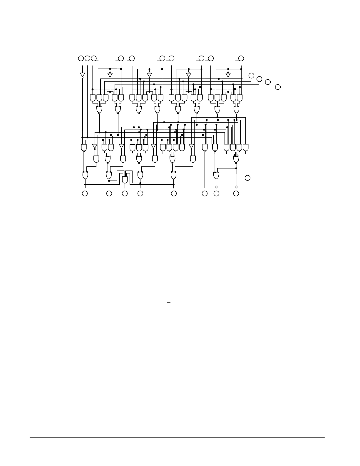
LOGIC DIAGRAM
SN54/74LS181
2
738
CnM
A
0
F
0
9 11 1610 13 15
1
B0A
1
F
1
14
F
A = B C
2
212223 20 1819
A
B
2
1
F
3
A
B
3
2
P
n+4
B
3
6
S
0
VCC = PIN 24
GND = PIN 12
= PIN NUMBERS
G
17
5
S
1
4
S
2
S
3
FUNCTIONAL DESCRIPTION
The SN54/74LS181 is a 4-bit high speed parallel Arithmetic
Logic Unit (ALU). Controlled by the four Function Select Inputs
(S0 . . . S3) and the Mode Control Input (M), it can perform all
the 16 possible logic operations or 16 different arithmetic
operations on active HIGH or active LOW operands. The
Function Table lists these operations.
When the Mode Control Input (M) is HIGH, all internal
carries are inhibited and the device performs logic operations
on the individual bits as listed. When the Mode Control Input is
LOW, the carries are enabled and the device performs
arithmetic operations on the two 4-bit words. The device
incorporates full internal carry lookahead and provides for
either ripple carry between devices using the C
output, or
n+4
for carry lookahead between packages using the signals P
(Carry Propagate) and G (Carry Generate), P and G are not
affected by carry in. When speed requirements are not
stringent, the LS181 can be used in a simple ripple carry mode
by connecting the Carry Output (C
) signal to the Carry Input
n+4
(Cn) of the next unit. For high speed operation the LS181 is
used in conjunction with the 9342 or 93S42 carry lookahead
circuit. One carry lookahead package is required for each
group of the four LS181 devices. Carry lookahead can be
provided at various levels and offers high speed capability
over extremely long word lengths.
The A = B output from the LS181 goes HIGH when all four F
outputs are HIGH and can be used to indicate logic
equivalence over four bits when the unit is in the subtract
mode. The A = B output is open collector and can be
wired-AND with other A = B outputs to give a comparison for
more then four bits. The A = B signal can also be used with the
C
signal to indicate A>B and A<B.
n+4
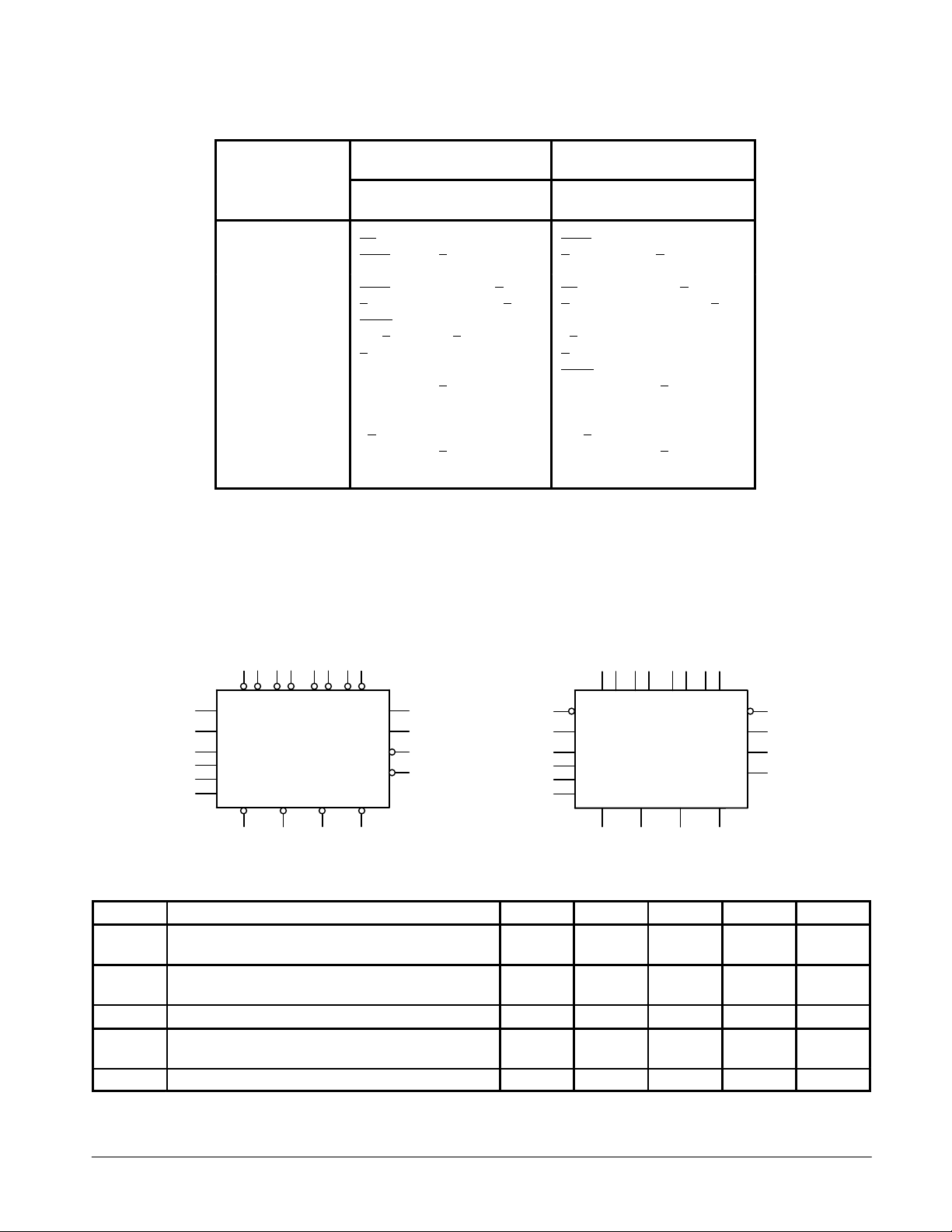
The Function Table lists the arithmetic operations that are
performed without a carry in. An incoming carry adds a one to
each operation. Thus, select code LHHL generates A minus B
minus 1 (2s complement notation) without a carry in and
generates A minus B when a carry is applied. Because
subtraction is actually performed by complementary addition
(1s complement), a carry out means borrow; thus a carry is
generated when there is no underflow and no carry is
generated when there is underflow.
As indicated, the LS181 can be used with either active LOW
inputs producing active LOW outputs or with active HIGH
inputs producing active HIGH outputs. For either case the
table lists the operations that are performed to the operands
labeled inside the logic symbol.
FAST AND LS TTL DATA
5-2
Page 3
SN54/74LS181
FUNCTION TABLE
MODE SELECT
INPUTS
S3S2S1S
L L L L A A minus 1 A A
L LLHAB AB minus 1 A + B A + B
L L H L A + B AB minus 1 AB A + B
L L H H Logical 1 minus 1 Logical 0 minus 1
L H L L A + B A plus (A + B)ABA plus AB
L HLHB AB plus (A + B)B (A + B) plus AB
L HHLA ⊕B A minus B minus 1 A ⊕ B A minus B minus 1
L H H H A + B A + B AB AB minus 1
H LLLAB A plus (A + B) A + B A plus AB
H LLHA ⊕B A plus B A ⊕ B A plus B
H LHLB AB plus (A + B) B (A + B) plus AB
H L H H A + B A + B AB AB minus 1
H H L L Logical 0 A plus A* Logical 1 A plus A*
H HLHAB AB plus A A + B (A + B) plus A
H HHLAB AB plus A A + B (A + B) Plus A
H H H H A A A A minus 1
L = LOW Voltage Level
H = HIGH Voltage Level
**Each bit is shifted to the next more significant position
**Arithmetic operations expressed in 2s complement notation
0
ACTIVE LOW INPUTS
& OUTPUTS
LOGIC
(M = H)
ARITHMETIC**
(M = L) (Cn = L)
ACTIVE HIGH INPUTS
& OUTPUTS
LOGIC
(M = H)
ARITHMETIC**
(M = L) (Cn = H)
LOGIC SYMBOLS
ACTIVE LOW OPERANDS ACTIVE HIGH OPERANDS
2 1 23 22 21 20 19 18
A0B0A1B1A2B2A3B
C
7
n
M
8
S
6
0
S
5
1
S
4
2
S
3
F
3
9101113
LS181
4 BIT ARITHMETIC
LOGIC UNIT
F
0
1
3
C
n+4
A = B
F
F
2
3
16
14
17
G
15
P
7
8
6
5
4
3
2 1 23 22 21 20 19 18
A0B0A1B1A2B2A3B
C
n
M
S
0
S
1
S
2
S
F
3
0
9101113
LS181
4 BIT ARITHMETIC
LOGIC UNIT
F
1F2
3
C
n+4
A = B
G
P
F
3
16
14
17
15
GUARANTEED OPERATING RANGES
Symbol Parameter Min Typ Max Unit
V
T
I
I
V
CC
A
OH
OL
OH
Supply Voltage 54
74
Operating Ambient Temperature Range 54
74
Output Current — High 54, 74 –0.4 mA
Output Current — Low 54
74
Output Voltage — High (A = B only) 54, 74 5.5 V
4.5
4.75
–55
0
5.0
5.0
25
25
5.5
5.25
125
70
4.0
8.0
V
°C
mA
FAST AND LS TTL DATA
5-3
Page 4
SN54/74LS181
VILI
LOW Volt
V
pg
VOHOutput HIGH Volt
CC
,
OH
,
IN IH
pg
VCC VCC MIN,
I
IH
pp y
I
A
V
MAX
S
1B
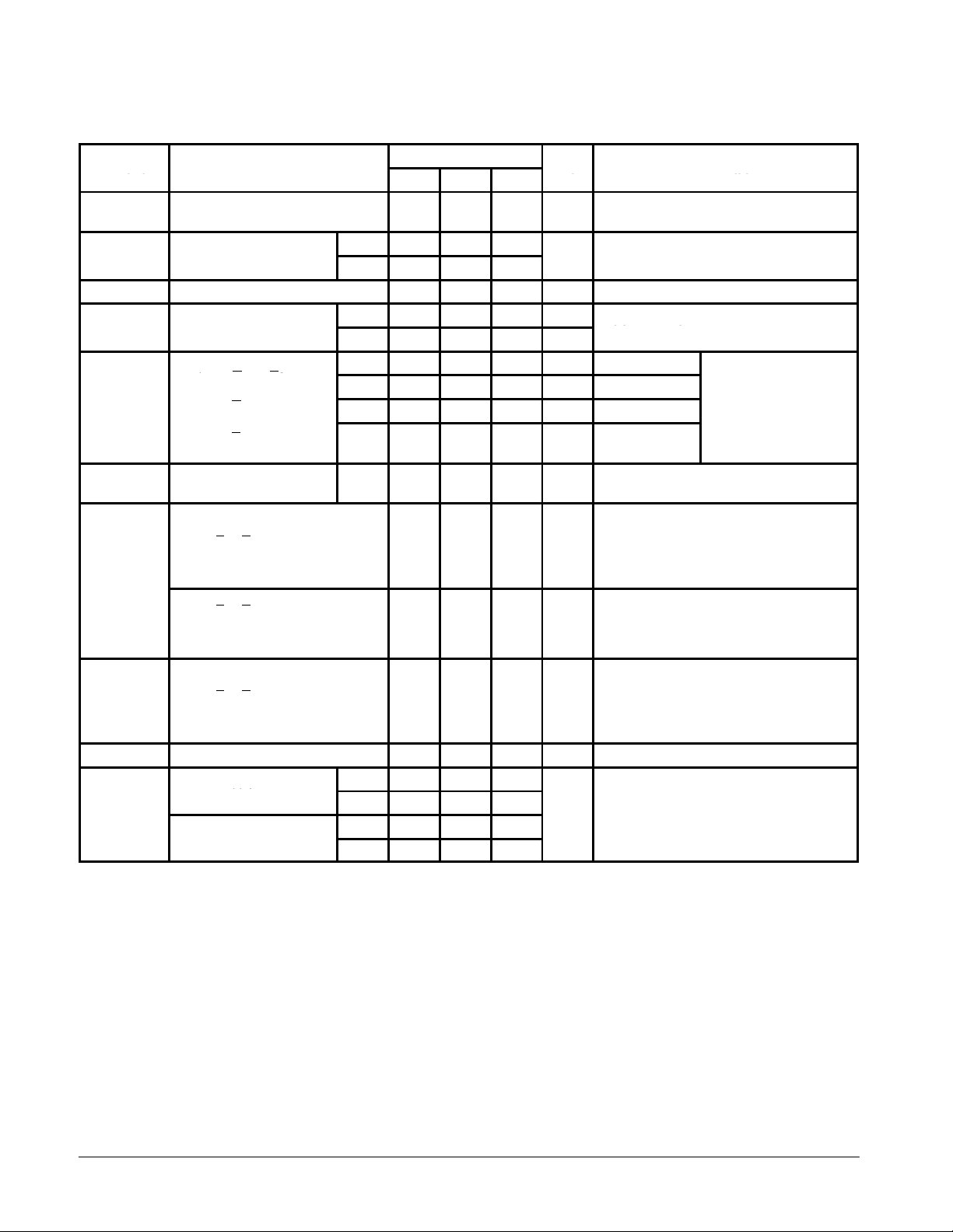
DC CHARACTERISTICS OVER OPERATING TEMPERATURE RANGE (unless otherwise specified)
Limits
Symbol Parameter
V
IH
V
IK
V
OL
I
OH
I
IH
I
IL
I
OS
CC
Note 1.
With outputs open, ICC is measured for the following conditions:
A. S0 through S3, M, and A inputs are at 4.5 V, all other inputs are grounded.
B. S0 through S3 and M are at 4.5 V, all other inputs are grounded.
Note 2: Not more than one output should be shorted at a time, nor for more than 1 second.
Input HIGH Voltage 2.0 V
nput
Input Clamp Diode Voltage –0.65 –1.5 V VCC = MIN, IIN = –18 mA
Output LOW Voltage
Except G and P
Output G 54, 74 0.7 V IOL = 16 mA
Output P
Output HIGH Current 54, 74 100 µA
Input HIGH Current
Mode Input
Any A
Any S Input
Cn Input
Mode Input
Any A
Any S Input
Cn Input
Input LOW Current
Mode Input
Any A
Any S Input
Cn Input
Short Circuit Current (Note 2) –20 –100 mA VCC = MAX
Power Supply Current
age
age
or B Input
or B Input
or B Input
See Note 1A
ee Note
54 0.7
74 0.8
54 2.5 3.5 V
74 2.7 3.5 V
54, 74 0.25 0.4 V IOL = 4.0 mA
74 0.35 0.5 V IOL = 8.0 mA
54
74
54 32
74 34
54 35
74 37
Min Typ Max
0.6
0.5
20
60
80
100
0.1
0.3
0.4
0.5
–0.4
–1.2
–1.6
–2.0
Unit T est Conditions
Guaranteed Input HIGH Voltage for
All Inputs
Guaranteed Input LOW Voltage for
All Inputs
VCC = MIN, IOH = MAX, VIN = V
or VIL per Truth Table
V IOL = 8.0 mA
VCC = MIN, IOH = MAX, VIN = V
or VIL per Truth Table
µA VCC = MAX, VIN = 2.7 V
mA VCC = MAX, VIN = 7.0 V
mA VCC = MAX, VIN = 0.4 V
m
CC
=
IH
VCC = VCC MIN,
VIN = VIL or V
per Truth Table
IH
IH
FAST AND LS TTL DATA
5-4
Page 5
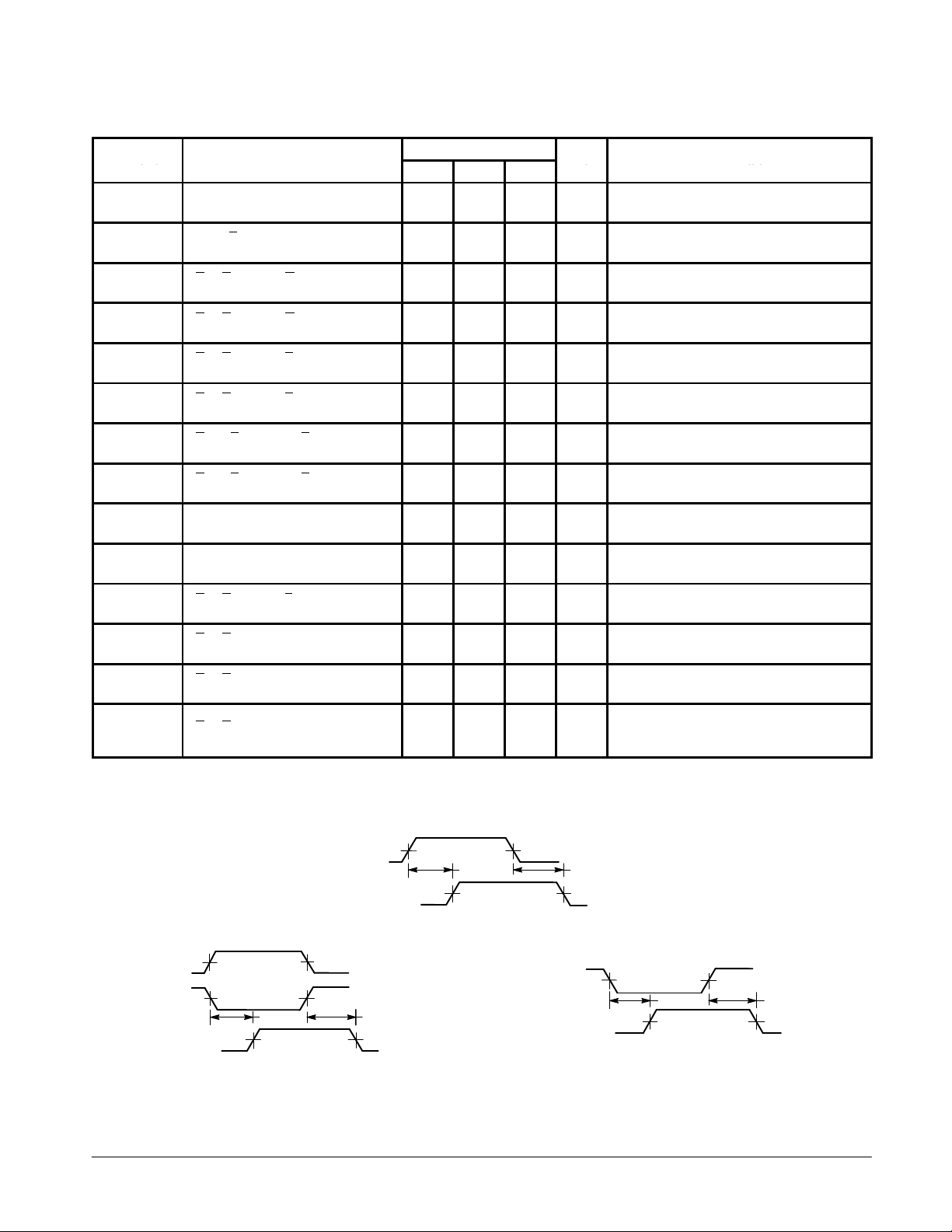
SN54/74LS181
AC CHARACTERISTICS (T
Symbol Parameter
t
PLH
t
PHL
t
PLH
t
PHL
t
PLH
t
PHL
t
PLH
t
PHL
t
PLH
t
PHL
t
PLH
t
PHL
t
PLH
t
PHL
t
PLH
t
PHL
t
PLH
t
PHL
t
PLH
t
PHL
t
PLH
t
PHL
t
PLH
t
PHL
t
PLH
t
PHL
t
PLH
t
PHL
Propagation Delay,
(Cn to C
(Cn to F Outputs)
(A or B Inputs to G Output)
(A or B Inputs to G Output)
(A or B Inputs to P Output)
(A or B Inputs to P Output)
(AX or BX Inputs to FX Output)
(AX or BX Inputs to FX Output)
(AX or BX Inputs to FXH Outputs)
(AX or BX Inputs to FXH Outputs)
(A or B Inputs to F Outputs)
(A or B Inputs to C
(A or B Inputs to C
(A or B Inputs to A = B Output)
n+4
)
= 25°C, VCC = 5.0 V, Pin 12 = GND, CL = 15 pF)
A
Limits
Min Typ Max
18
13
17
13
19
15
21
21
20
20
20
22
21
13
21
21
22
26
n+4
n+4
Output)
Output)
25
25
27
27
33
41
Unit Test Conditions
27
20
26
20
29
23
32
32
30
30
30
33
32
20
32
32
38
26
38
38
33
38
38
38
41
41
50
62
M = 0 V, (Sum or Diff Mode)
ns
See Fig. 4 and Tables I and II
M = 0 V, (Sum Mode)
ns
See Fig. 4 and Table I
M = S1 = S2 = 0 V, S0 = S3 = 4.5 V
ns
(Sum Mode) See Fig. 4 and Table I
M = S0 = S3 = 0 V, S1 = S2 = 4.5 V
ns
(Diff Mode) See Fig. 5 and Table II
M = S1 = S2 = 0 V, S0 = S3 = 4.5 V
ns
(Sum Mode) See Fig. 4 and Table I
M = S0 = S3 = 0 V, S1 = S2 = 4.5 V
ns
(Diff Mode) See Fig. 5 and Table II
M = S1 = S2 = 0 V, S0 = S3 = 4.5 V
ns
(Sum Mode) See Fig. 4 and Table I
M = S0 = S3 = 0 V, S1 = S2 = 4.5 V
ns
(Diff Mode) See Fig. 5 and Table II
M = S1 = S2 = 0 V, S0 = S3 = 4.5 V
ns
(Sum Mode) See Fig. 4 and Table I
M = S0 = S3 = 0 V, S1 = S2 = 4.5 V
ns
(Diff Mode) See Fig. 5 and Table II
M = 4.5 V (Logic Mode)
ns
See Fig. 4 and Table III
M = 0 V, S0 = S3 = 4.5 V, S1 = S2 = 0 V
ns
(Sum Mode) See Fig. 6 and Table I
M = 0 V, S0 = S3 = 0 V, S1 = S2 = 4.5 V
ns
(Diff Mode)
M = S0 = S3 = 0 V, S1 = S2 = 4.5 V
RL = 2.0 kΩ
ns
(Diff Mode) See Fig. 5 and Table II
A INPUT
B INPUT
OUTPUT
AC WAVEFORMS
INPUT
1.3 V 1.3 V
t
PLH
OUTPUT
t
PHL
1.3 V1.3 V
Figure 4
1.3 V 1.3 V
1.3 V 1.3 V
OUTPUT
t
PLH
t
PLH
INPUT
1.3 V1.3 V
t
PHL
1.3 V1.3 V
Figure 5 Figure 6
FAST AND LS TTL DATA
5-5
t
PHL
1.3 V1.3 V
Page 6
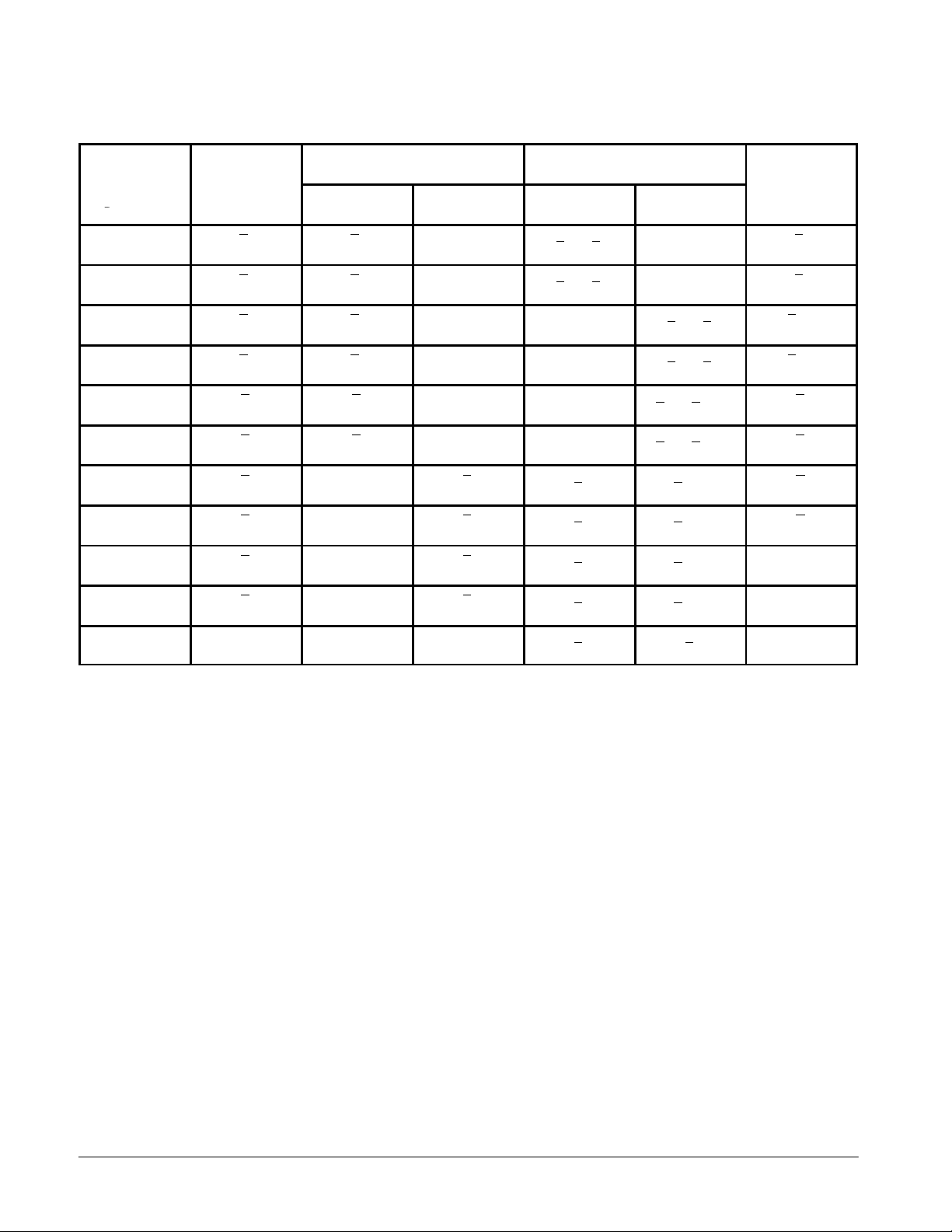
SN54/74LS181
Input
Output
SUM MODE TEST TABLE I FUNCTION INPUTS: S
Other Input
Parameter
t
PLH
t
PHL
t
PLH
t
PHL
t
PLH
t
PHL
t
PLH
t
PHL
t
PLH
t
PHL
t
PLH
t
PHL
t
PLH
t
PHL
t
PLH
t
PHL
t
PLH
t
PHL
t
PLH
t
PHL
t
PLH
t
PHL
Same Bit
Under
Test
A
l
B
l
A
l
B
l
A B None None
B A None None
A None B
B None A
A None B
B None A
C
n
Apply
4.5 V
B
l
A
l
B
l
A
l
None None
Apply
GND
None
None
None C
None C
Other Data Inputs
Apply
4.5 V
Remaining
A and B
Remaining
A and B
n
n
Remaining
B
Remaining
B
Remaining
B
Remaining
B
All
A
Remaining
Remaining
Remaining
A and B, C
Remaining
A
Remaining
Remaining
Remaining
Remaining
= S3 = 4.5 V, S1 = S2 = M = 0 V
0
Apply
GND
C
n
C
n
A
and B
A
and B
and B, C
A
, C
n
A
, C
n
A, C
n
A
, C
n
All
B
n
n
Under
Test
F
F
F
l+1
F
l+1
P
P
G
G
C
n+4
C
n+4
Any F
or C
l
l
n+4
FAST AND LS TTL DATA
5-6
Page 7
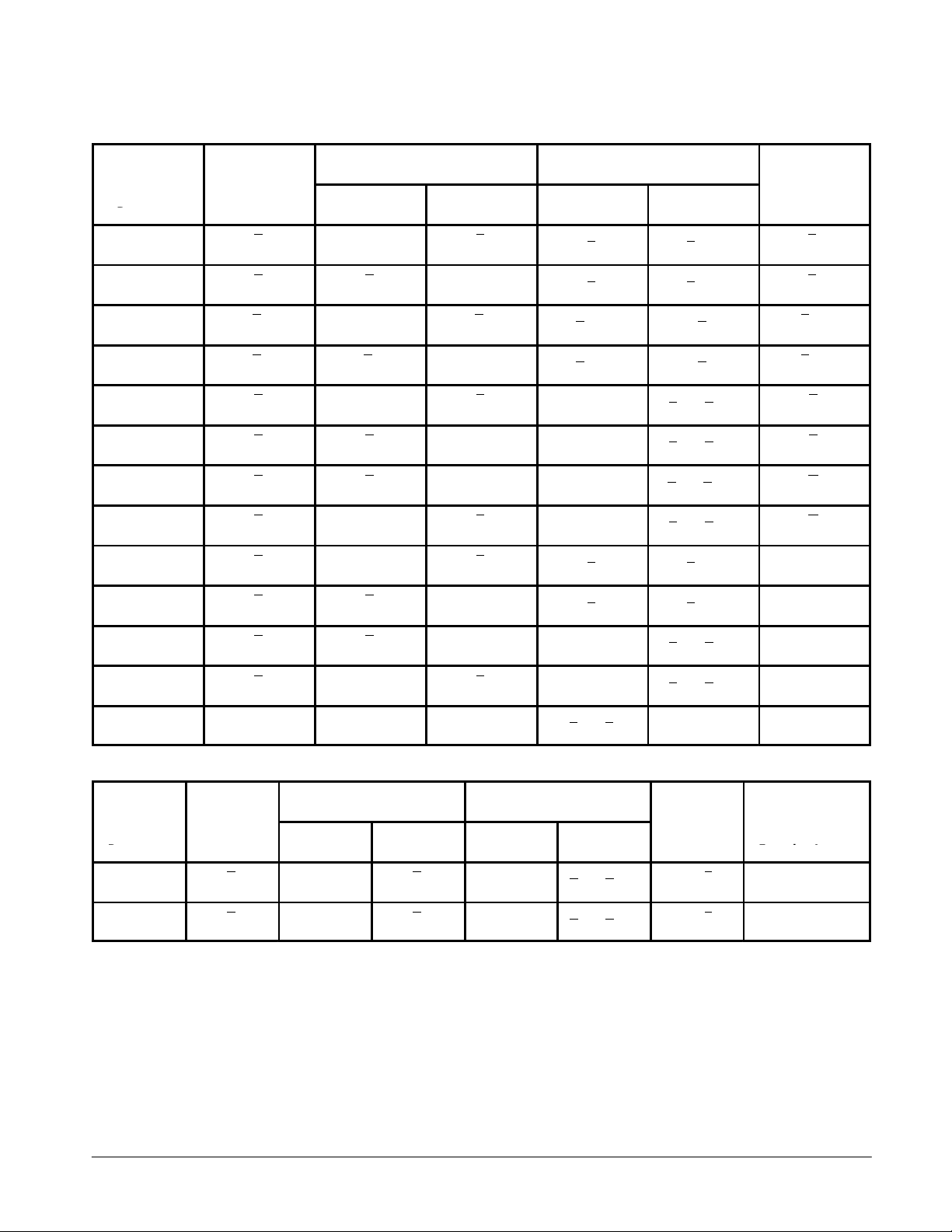
SN54/74LS181
Input
Output
Input
Output
DIFF MODE TEST TABLE II FUNCTION INPUTS: S
Other Input
Parameter
t
PLH
t
PHL
t
PLH
t
PHL
t
PLH
t
PHL
t
PLH
t
PHL
t
PLH
t
PHL
t
PLH
t
PHL
t
PLH
t
PHL
t
PLH
t
PHL
t
PLH
t
PHL
t
PLH
t
PHL
t
PLH
t
PHL
t
PLH
t
PHL
t
PLH
t
PHL
Same Bit
Under
Test
A None B
B A None
A
l
B
l
A None B None
B A None None
A B None None
B None A None
A None B
B A None
A B None None
B None A None
C
n
Apply
4.5 V
None B
A
l
None None
Apply
GND
l
None
Other Data Inputs
Apply
4.5 V
Remaining
A
Remaining
A
Remaining
B
, C
n
Remaining
B
, C
n
Remaining
A
Remaining
A
All
A and B
Remaining
Remaining
Remaining
Remaining
Remaining
A and B, C
Remaining
A
Remaining
A
Remaining
A
Remaining
Remaining
Remaining
A
Remaining
A and B, C
= S2 = 4.5 V, S0 = S3 = M = 0 V
1
Apply
GND
B, C
n
B, C
n
A
A
n
and B, C
and Bl, C
and B, C
and B, C
n
n
n
B, C
n
B
, C
n
n
n
None C
Under
Test
F
l
F
l
F
l+1
F
l+1
P
P
G
G
A = B
A = B
c
n+4
C
n+4
n+4
LOGIC MODE TEST TABLE III
Under
Parameter
t
PLH
t
PHL
t
PLH
t
PHL
Test
A None B None
B None A None
Apply
4.5 V
Other Input
Same Bit
Other Data Inputs
Apply
GND
Apply
4.5 V
FAST AND LS TTL DATA
5-7
Apply
GND
Remaining
A
and B, C
Remaining
A and B, C
Under
Test
n
n
Any F
Any F
Function Inputs
S1 = S2 = M = 4.5 V
S0 = S3 = 0 V
S1 = S2 = M = 4.5 V
S0 = S3 = 0 V
 Loading...