

Page 1
SN54/74LS168
BCD DECADE/MODULO
16 BINARY SYNCHRONOUS
BI-DIRECTIONAL COUNTERS
The SN54 / 74LS168 and SN54 / 74LS169 are fully synchronous 4-stage
up/down counters featuring a preset capability for programmable operation,
carry lookahead for easy cascading and a U/D input to control the direction
of counting. The SN54/74LS168 counts in a BCD decade (8, 4, 2, 1)
sequence, while the SN54/74LS169 operates in a Modulo 16 binary
sequence. All state changes, whether in counting or parallel loading, are
initiated by the LOW-to-HIGH transition of the clock.
• Low Power Dissipation 100 mW Typical
• High-Speed Count Frequency 30 MHz Typical
• Fully Synchronous Operation
• Full Carry Lookahead for Easy Cascading
• Single Up/Down Control Input
• Positive Edge-Trigger Operation
• Input Clamp Diodes Limit High-Speed Termination Effects
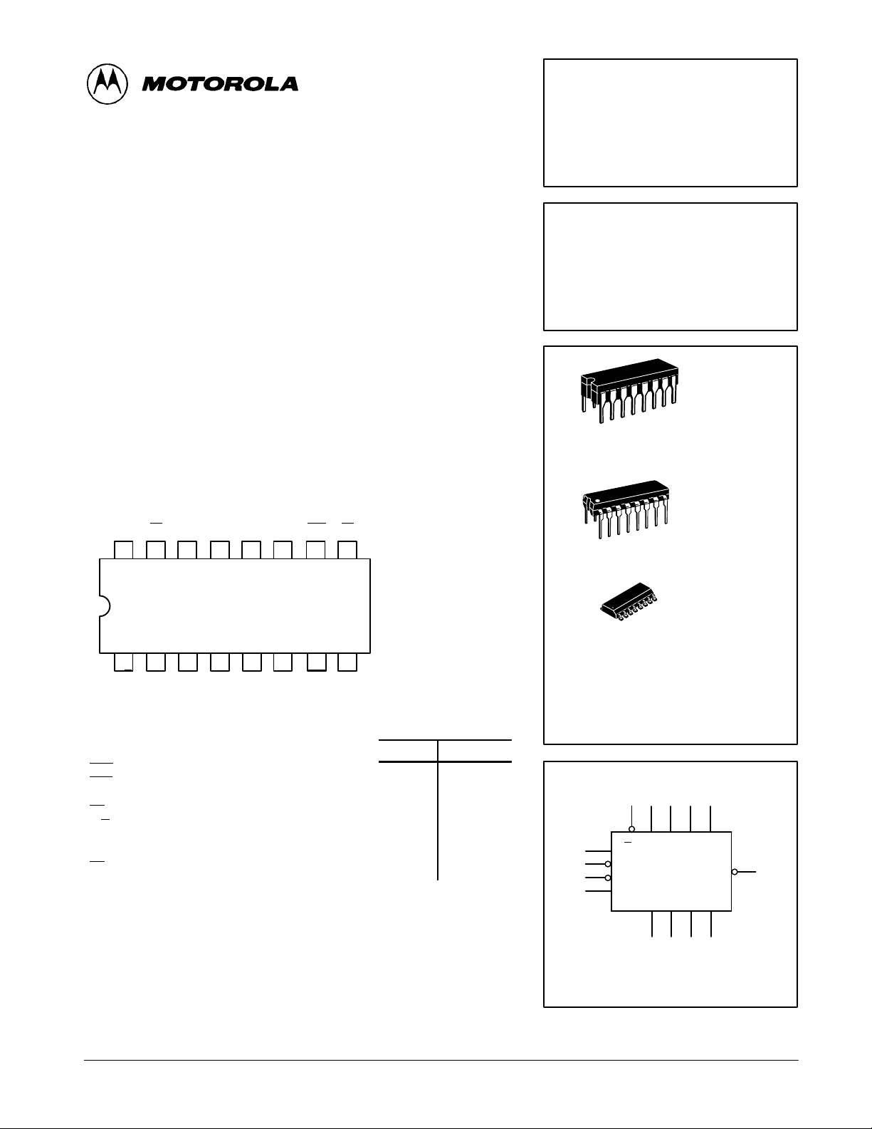
CONNECTION DIAGRAM DIP (TOP VIEW)
TC Q0Q1Q
V
CC
16 15
2
14 13 12 11 10 9
CETQ
3
PE
SN54/74LS169
BCD DECADE/MODULO
16 BINARY SYNCHRONOUS
BI-DIRECTIONAL COUNTERS
LOW POWER SCHOTTKY
J SUFFIX
CERAMIC
16
1
16
1
CASE 620-09
N SUFFIX
PLASTIC
CASE 648-08
NOTE:
The Flatpak version
has the same pinouts
(Connection Diagram) as
the Dual In-Line Package.
123456
CP P0P1P2P3CEP GND
U/D
PIN NAMES LOADING (Note a)
CEP
CET
CP
PE
U/D
P0–P
Q0–Q
TC
NOTES:
a. 1 TTL Unit Load (U.L.) = 40 µA HIGH/1.6 mA LOW.
b. The Output LOW drive factor is 2.5 U.L. for Military (54) and 5 U.L. for Commercial (74)
b. T emperature Ranges.
Count Enable Parallel (Active LOW) Input
Count Enable Trickle (Active LOW) Input
Clock Pulse (Active positive going edge) Input
Parallel Enable (Active LOW) Input
Up-Down Count Control Input
Parallel Data Inputs
3
Flip-Flop Outputs
3
Terminal Count (Active LOW) Output
7
8
HIGH
0.5 U.L.
1.0 U.L.
0.5 U.L.
0.5 U.L.
0.5 U.L.
0.5 U.L.
10 U.L.
10 U.L.
LOW
0.25 U.L.
0.5 U.L.
0.25 U.L.
0.25 U.L.
0.25 U.L.
0.25 U.L.
5 (2.5) U.L.
5 (2.5) U.L.
16
1
CASE 751B-03
ORDERING INFORMATION
SN54LSXXXJ Ceramic
SN74LSXXXN Plastic
SN74LSXXXD SOIC
LOGIC SYMBOL
934 56
1
7
10
2
PE P0P1P2P
U/D
CEP
CET
CP
Q0Q1Q2Q
14 13 12 11
VCC = PIN 16
GND = PIN 8
D SUFFIX
SOIC
3
TC
3
15
FAST AND LS TTL DAT A
5-1
Page 2
SN54/74LS168 • SN54/74LS169
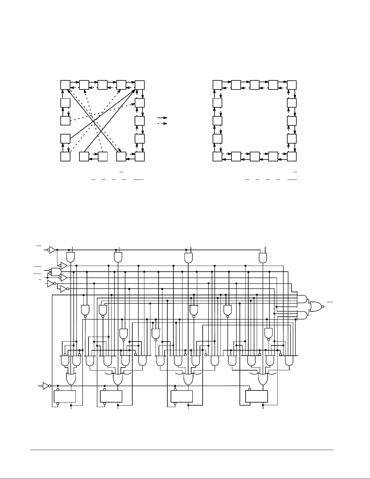
STATE DIAGRAMS
PE
UP/DOWN DECADE COUNTER
SN54/74LS168
0123
15
14
13
12
SN54/74LS168
UP: TC = Q0 ⋅ Q3 ⋅ (U/D
DOWN: TC = Q
P
0
⋅ Q1 ⋅ Q2 ⋅ Q3 ⋅ (U/D)
0
)
P
1
4
5
6
7
891011
Count Up
Count Down
LOGIC DIAGRAMS
SN54/74LS168
P
2
SN54/74LS169
0123
15
14
13
12
SN54/74LS169
UP: TC = Q0 ⋅ Q1 ⋅ Q2 ⋅ Q3 ⋅ (U/D
DOWN: TC = Q
⋅ Q1 ⋅ Q2 ⋅ Q3 ⋅ (U/D)
0
P
3
4
5
6
7
891011
)
CEP
CET
CP
U/D
CP D
Q
TC
0
Q
1
Q
2
Q
3
FAST AND LS TTL DATA
5-2
Page 3
SN54/74LS168 • SN54/74LS169
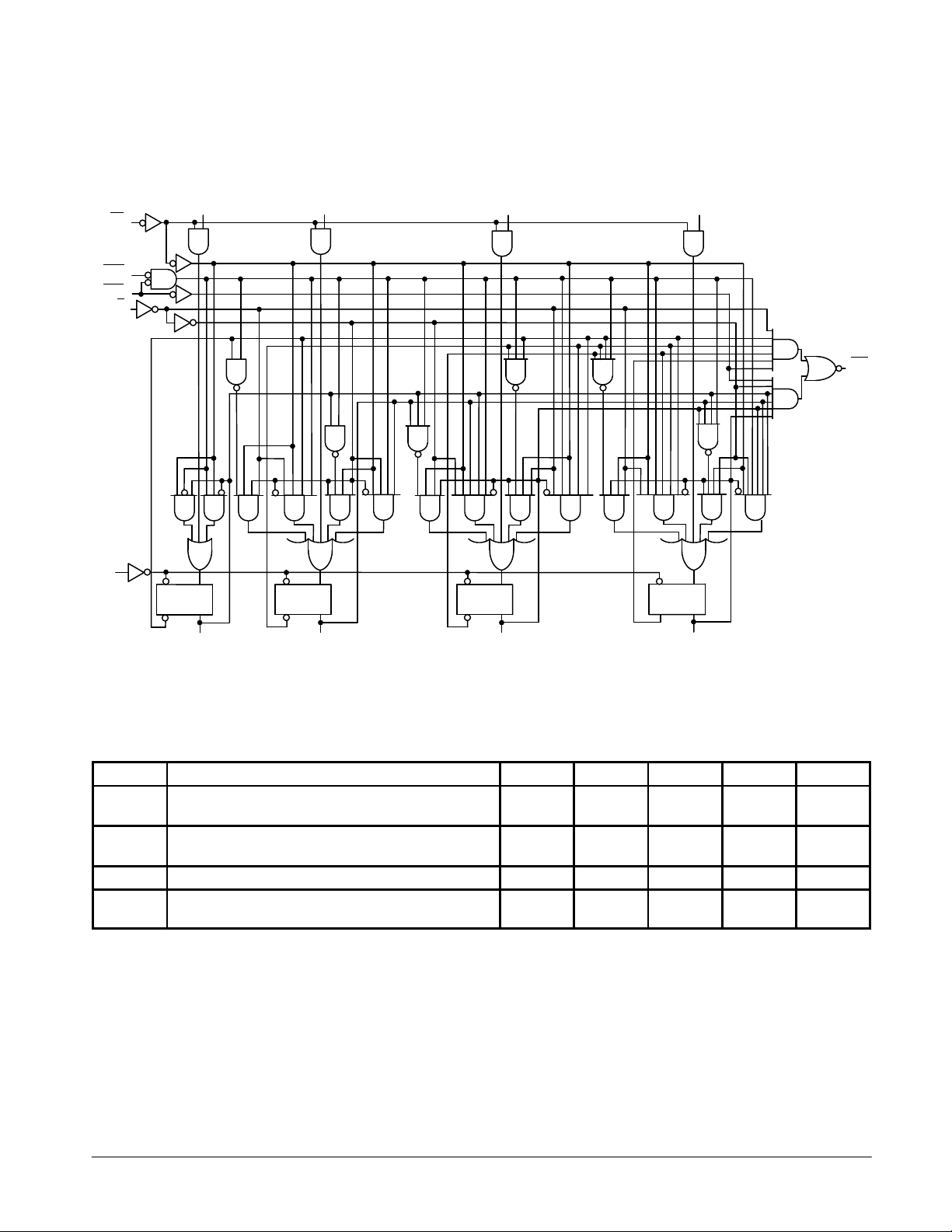
LOGIC DIAGRAMS (continued)
SN54/74LS169
CEP
CET
U/D
CP
PE
CP D
Q
P
0
0
P
1
Q
1
P
2
Q
2
P
3
TC
Q
3
GUARANTEED OPERATING RANGES
Symbol Parameter Min Typ Max Unit
V
T
I
OH
I
OL
CC
A
Supply Voltage 54
74
Operating Ambient Temperature Range 54
74
Output Current — High 54, 74 –0.4 mA
Output Current — Low 54
74
4.5
4.75
–55
0
5.0
5.0
25
25
5.5
5.25
125
70
4.0
8.0
FAST AND LS TTL DATA
5-3
V
°C
mA
Page 4
SN54/74LS168 • SN54/74LS169
VILI
LOW Volt
V
pg
VOHOutput HIGH Volt
CC
,
OH
,
IN IH
VOLOutput LOW Volt
V
V
V
I
IH
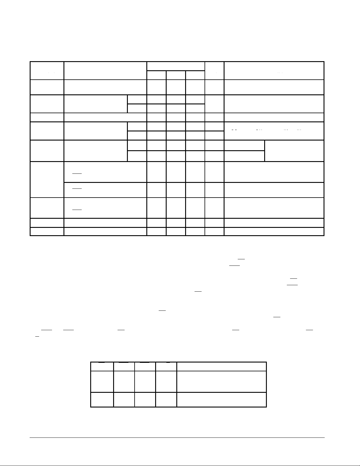
DC CHARACTERISTICS OVER OPERATING TEMPERATURE RANGE (unless otherwise specified)
Limits
Symbol Parameter
V
IH
V
IK
I
IH
I
IL
I
OS
I
CC
Note 1: Not more than one output should be shorted at one time, nor for more than 1 second.
Input HIGH Voltage 2.0 V
nput
Input Clamp Diode Voltage –0.65 –1.5 V VCC = MIN, IIN = –18 mA
Input HIGH Current
Other Inputs
CET
Other Input
CET
Input LOW Current
Other Input
CET
Short Circuit Current (Note 1) –20 –100 mA VCC = MAX
Power Supply Current 34 mA VCC = MAX
age
age
age
Input
Input
Input
54 0.7
74 0.8
54 2.5 3.5 V
74 2.7 3.5 V
54, 74 0.25 0.4 V IOL = 4.0 mA
74 0.35 0.5 V IOL = 8.0 mA
Min Typ Max
20
40
0.1
0.2
–0.4
–0.8
Unit Test Conditions
Guaranteed Input HIGH Voltage for
All Inputs
Guaranteed Input LOW Voltage for
All Inputs
VCC = MIN, IOH = MAX, VIN = V
or VIL per Truth Table
µA VCC = MAX, VIN = 2.7 V
mA VCC = MAX, VIN = 7.0 V
mA VCC = MAX, VIN = 0.4 V
IH
VCC = VCC MIN,
=
or
IN
IL
per Truth Table
IH
FUNCTIONAL DESCRIPTION
The SN54/74LS168 and SN54/74LS169 use edgetriggered D-type flip-flops that have no constraints on
changing the control or data input signals in either state of the
Clock. The only requirement is that the various inputs attain
the desired state at least a set-up time before the rising edge of
the clock and remain valid for the recommended hold time
thereafter.
The parallel load operation takes precedence over the other
operations, as indicated in the Mode Select T able. When PE
is
LOW, the data on the P0–P3 inputs enters the flip-flops on the
next rising edge of the Clock. In order for counting to occur,
both CEP
U/D
and CET must be LOW and PE must be HIGH. The
input then determines the direction of counting.
MODE SELECT TABLE
PE CEP CET U/D Action on Rising Clock Edge
L X X X Load (Pn → Qn)
H L L H Count Up (increment)
H L L L Count Down (decrement)
H H X X No Change (Hold)
H X H X No Change (Hold)
H = HIGH Voltage Level
L = LOW Voltage Level
X = Immaterial
The T erminal Count (TC
LOW, provided that CET
) output is normally HIGH and goes
is LOW, when a counter reaches zero
in the COUNT DOWN mode or reaches 15 (9 for the
SN54/74LS168) in the COUNT UP mode. The TC
is not a function of the Count Enable Parallel (CEP
output of the SN54/74LS168 decade counter can also
The TC
output state
) input level.
be LOW in the illegal states 11, 13 and 15, which can occur
when power is turned on or via parallel loading. If illegal state
occurs, the SN54/74LS168 will return to the legitimate
sequence within two counts. Since the TC
signal is derived by
decoding the flip-flop states, there exists the possibility of
decoding spikes on TC
. For this reason the use of TC as a
clock signal is not recommended.
FAST AND LS TTL DATA
5-4
Page 5
SN54/74LS168 • SN54/74LS169
C
L
pF
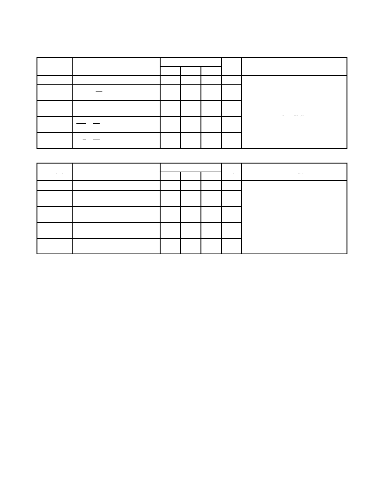
AC CHARACTERISTICS (T
Symbol Parameter
f
MAX
t
PLH
t
PHL
t
PLH
t
PHL
t
PLH
t
PHL
t
PLH
t
PHL
Maximum Clock Frequency 25 32 MHz
Propagation Delay,
Clock to TC
Propagation Delay,
Clock to any Q
Propagation Delay,
CET
to TC
Propagation Delay,
U/D to TC
= 25°C, VCC = 5.0 V)
A
AC SETUP REQUIREMENTS (T
Symbol Parameter
t
W
t
s
t
s
t
s
t
h
Clock Pulse Width 25 ns
Setup Time,
Data or Enable
Setup Time
PE
Setup Time
U/D
Hold Time
Any Input
= 25°C)
A
Limits
Min Typ Max
23
23
13
15
15
15
17
19
Limits
Min Typ Max
20 ns
25 ns
30 ns
0 ns
35
35
20
23
20
20
25
29
Unit Test Conditions
ns
ns
ns
ns
Unit Test Conditions
VCC = 5.0 V
C
= 15 pF
= 15
VCC = 5.0 V
FAST AND LS TTL DATA
5-5
Page 6
CP
Q OR TC
SN54/74LS168 • SN54/74LS169
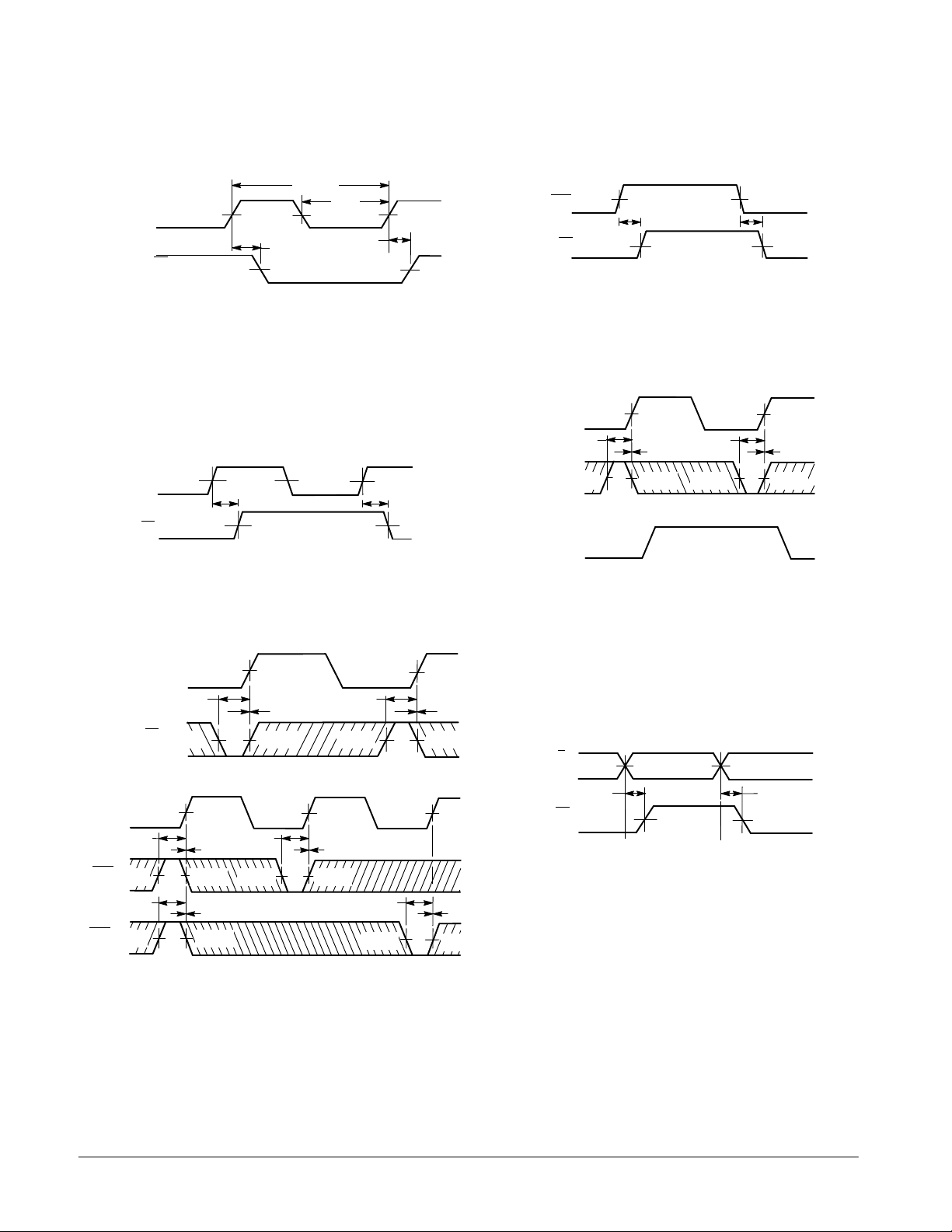
AC WAVEFORMS
1/f
max
t
W
1.3 V 1.3 V
1.3 V
t
t
PHL
1.3 V 1.3 V
PLH
CET
TC
1.3 V 1.3 V
t
PLH
1.3 V
t
PHL
1.3 V
CP
TC
SR OR PE
Figure 1. Clock to Output Delays,
Count Frequency , and Clock Pulse Width
1.3 V 1.3 V 1.3 V
t
PLH
1.3 V 1.3 V
t
PHL
Q0
•
Q1 • Q2 • Q
Figure 2. Count Enable Trickle Input
To Terminal Count Output Delays
CP
ts(H)
3
3
1.3 V 1.3 V
ts(L)
1.3 V 1.3 V1.3 V1.3 VP0 • P1 • P2 • P
Figure 3. Clock to T erminal Delays Figure 4. Setup Time (ts) and Hold (th)
for Parallel Data Inputs
CP
t
s(L)
1.3 V 1.3 V1.3 V1.3 V
1.3 V
th(L) = 0 th(H) = 0
ts(H)
1.3 V
U/D
1.3 V 1.3 V
th(L) = 0th(H) = 0
CP
ts(H)
CEP
1.3 V 1.3 V
ts(H)
1.3 V
CET
1.3 V 1.3 V 1.3 V
ts(L)
th(H) = 0 th(L) = 0
1.3 V
The shaded areas indicate when the
input is permitted to change for
predictable output performance.
th(L) = 0th(H) = 0
1.3 V1.3 V
ts(L)
1.3 V
Figure 5. Setup Time and Hold Time for
Count Enable and Parallel Enable Inputs,
and Up-Down Control Inputs
FAST AND LS TTL DATA
1.3 V
5-6
t
PLH
TC
1.3 V 1.3 V
Figure 6. Up-Down Input to
Terminal Count Output Delays
t
PHL
 Loading...