

Page 1
8-BIT SHIFT REGISTERS
CLEAR
CLOCK
SERIAL
Q
H
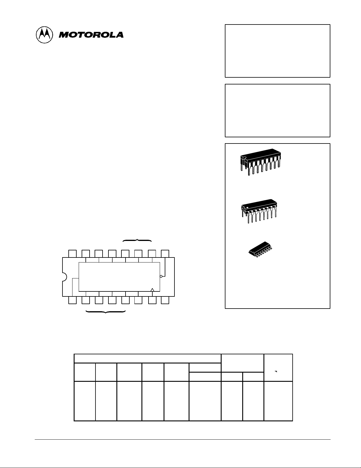
The SN54L/ 74LS166 is an 8-Bit Shift Register. Designed with all inputs
buffered, the drive requirements are lowered to one 54/74LS standard load.
By utilizing input clamping diodes, switching transients are minimized and
system design simplified.
The LS166 is a parallel-in or serial-in, serial-out shift register and has a
complexity of 77 equivalent gates with gated clock inputs and an overriding
clear input. The shift/load input establishes the parallel-in or serial-in mode.
When high, this input enables the serial data input and couples the eight
flip-flops for serial shifting with each clock pulse. Synchronous loading occurs
on the next clock pulse when this is low and the parallel data inputs are
enabled. Serial data flow is inhibited during parallel loading. Clocking is done
on the low-to-high level edge of the clock pulse via a two input positive NOR
gate, which permits one input to be used as a clock enable or clock inhibit
function. Clocking is inhibited when either of the clock inputs are held high,
holding either input low enables the other clock input. This will allow the
system clock to be free running and the register stopped on command with
the other clock input. A change from low-to-high on the clock inhibit input
should only be done when the clock input is high. A buffered direct clear input
overrides all other inputs, including the clock, and sets all flip-flops to zero.
• Synchronous Load
• Direct Overriding Clear
• Parallel to Serial Conversion
PARALLEL PARALLEL INPUTS
INPUT OUTPUT
SHIFT/
V
LOAD
CC
16 15
123456
SERIAL
INPUT
HQ
14 13 12 11 10 9
SHIFT/
HQ
LOAD
SERIAL INPUT
ABC D
A B C D CLOCK
PARALLEL INPUTS
GEF CLEAR
H
GFE
H
CLOCK
INHIBIT
INHIBIT
CLEAR
CK
8
7
CLOCK GND
SN54/74LS166
8-BIT SHIFT REGISTERS
LOW POWER SCHOTTKY
J SUFFIX
CERAMIC
16
1
16
1
16
1
ORDERING INFORMATION
SN54LSXXXJ Ceramic
SN74LSXXXN Plastic
SN74LSXXXD SOIC
CASE 620-09
N SUFFIX
PLASTIC
CASE 648-08
D SUFFIX
SOIC
CASE 751B-03
FUNCTION TABLE
INPUTS
SHIFT/ CLOCK
LOAD INHIBIT
L X X X X X L L L
H X L L X X Q
H L L ↑ X a . . . h a b h
H H L ↑ H X H Q
H H L ↑ L X L Q
H X H ↑ X X Q
PARALLEL
A . . . H Q
INTERNAL
OUTPUTS
A
A0
A0
Q
Q
Q
B0
An
An
B0
OUTPUT
Q
B
Q
Q
Q
Q
FAST AND LS TTL DAT A
5-1
H0
Gn
Gn
H0
Page 2
SN54/74LS166
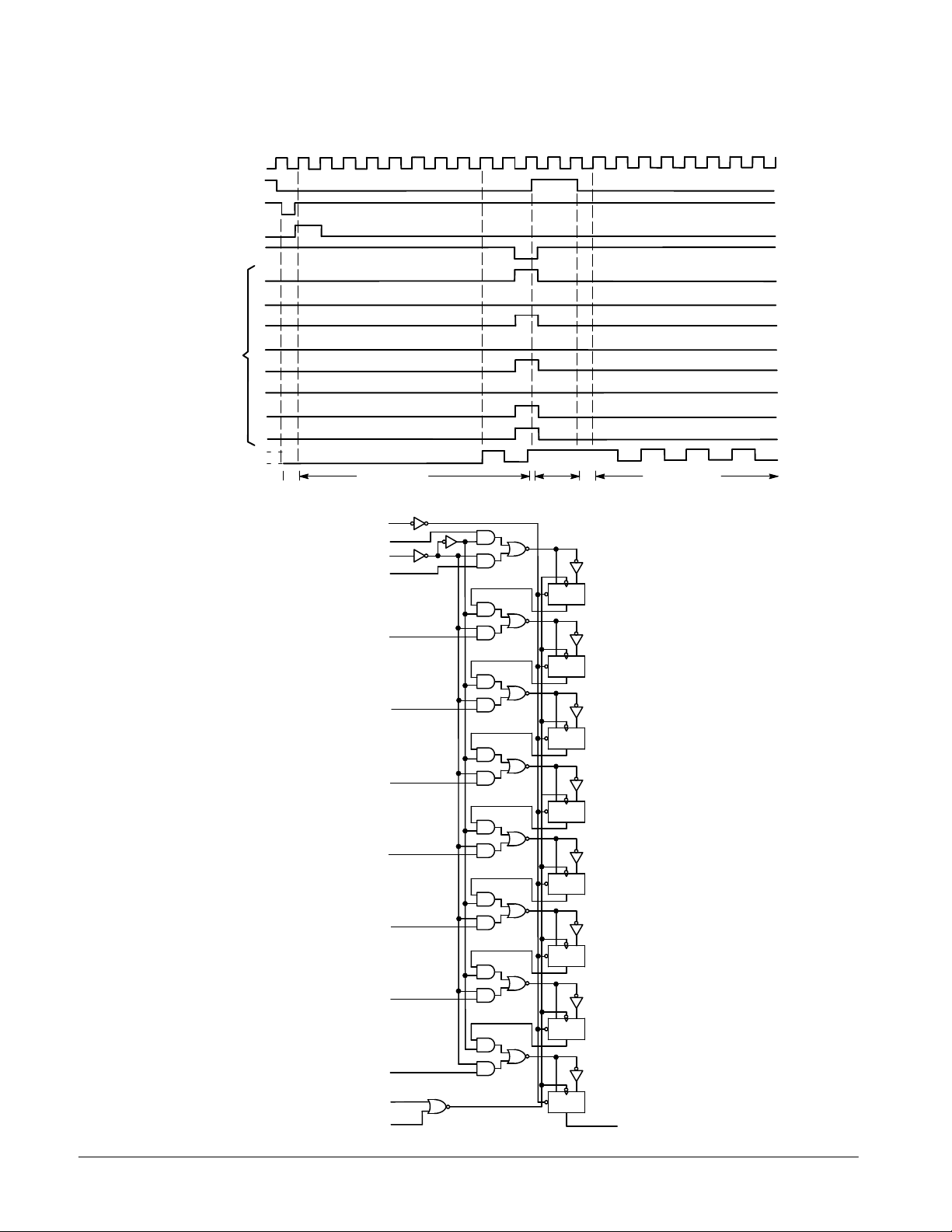
T ypical Clear, Shift, Load, Inhibit, and Shift Sequences
CLOCK
CLOCK INIHIBIT
CLEAR
SERIAL INPUT
SHIFT/LOAD
A
B
C
PARALLEL
INPUTS
OUTPUT Q
D
E
F
G
H
H
CLEAR
SERIAL SHIFT
CLEAR
SERIAL INPUT
SHIFT/LOAD
A
B
C
D
E
F
G
H
CLOCK
CLOCK INHIBIT
(9)
(1)
(15)
(2)
(3)
(4)
(5)
(10)
(11)
(12)
(14)
(7)
(6)
H
L
H
L
H
L
H
H
LOAD
INHIBIT
RCKS
RCKS
RCKS
RCKS
RCKS
RCKS
RCKS
RCKS
Q
A
Q
B
Q
C
Q
D
Q
E
Q
F
Q
G
(13)
SERIAL SHIFT
Q
H
LL
HH H H H
L
FAST AND LS TTL DATA
5-2
Page 3
SN54/74LS166
VILI
LOW Volt
V
pg
VOHOutput HIGH Volt
CC
,
OH
,
IN IH
VOLOutput LOW Volt
V
V
V
IIHI
HIGH C
t
GUARANTEED OPERATING RANGES
Symbol Parameter Min Typ Max Unit
V
CC
T
A
I
OH
I
OL
DC CHARACTERISTICS OVER OPERATING TEMPERATURE RANGE (unless otherwise specified)
Symbol Parameter
V
IH
V
IK
I
IL
I
OS
I
CC
Note 1: Not more than one output should be shorted at a time, nor for more than 1 second.
Supply Voltage 54
Operating Ambient Temperature Range 54
Output Current — High 54, 74 –0.4 mA
Output Current — Low 54
Limits
Min Typ Max
Input HIGH Voltage 2.0 V
nput
Input Clamp Diode Voltage –0.65 –1.5 V VCC = MIN, IIN = –18 mA
nput
Input LOW Current –0.4 mA VCC = MAX, VIN = 0.4 V
Short Circuit Current (Note 1) –20 –100 mA VCC = MAX
Power Supply Current 38 mA VCC = MAX
age
age
age
urren
54 0.7
74 0.8
54 2.5 3.5 V
74 2.7 3.5 V
54, 74 0.25 0.4 V IOL = 4.0 mA
74 0.35 0.5 V IOL = 8.0 mA
74
74
74
20 µA VCC = MAX, VIN = 2.7 V
0.1 mA VCC = MAX, VIN = 7.0 V
4.5
4.75
–55
0
Unit Test Conditions
Guaranteed Input HIGH Voltage for
All Inputs
Guaranteed Input LOW Voltage for
All Inputs
VCC = MIN, IOH = MAX, VIN = V
or VIL per Truth Table
5.0
5.0
25
25
5.5
5.25
125
70
4.0
8.0
VCC = VCC MIN,
=
IN
IL
per Truth Table
or
IH
IH
V
°C
mA
FAST AND LS TTL DATA
5-3
Page 4
CLEAR INPUT
V
V
CLOCK INPUT
DATA
INPUT
(SEE TEST
TABLE)
OUTPUT Q
V
V
ref
t
PHL
(clear-Q)
SN54/74LS166
TEST TABLE FOR SYNCHRONOUS INPUTS
DATA INPUT
FOR TEST
H 0 V QH at t
Serial
Input
t
w(clear)
ref
t
w(clock)
V
ref
SHIFT/LOAD OUTPUT TESTED
4.5 V QH at t
AC WAVEFORMS
V
ref
tn +
1
V
ref
t
PLH
t
V
ref
(SEE NOTE 1)
h
V
ref
t
n
V
ref
t
su
V
ref
(CLK-Q)
n+1
n+8
t
n
t
su
tn +
1
V
ref
V
t
PHL
(CLK-Q)
ref
3 V
0 V
3 V
t
h
V
ref
0 V
3 V
0 V
V
V
OH
OL
AC CHARACTERISTICS (T
Symbol Parameter
f
MAX
t
PHL
t
PLH
t
PHL
Maximum Clock Frequency 25 35 MHz
Clear to Output 19 30 ns
Clock to Output
= 25°C)
A
AC SETUP REQUIREMENTS (T
Symbol Parameter
t
W
t
s
t
s
t
h
Clock Clear Pulse Width 30 ns
Mode Control Setup Time 30 ns
Data Setup Time 20 ns
Hold Time, Any Input 15 ns
= 25°C)
A
NOTE 1. tn = bit time before clocking transition
NOTE 1. t
NOTE 1. t
NOTE 1. LS166 V
= bit time after one clocking transition
n+1
= bit time after eight clocking transition
n+8
Min Typ Max
Min Typ Max
ref
Limits
23
24
Limits
= 1.3 V.
35
35
Unit Test Conditions
ns
Unit Test Conditions
VCC = 5.0 V
CL = 15 pF
= 5.0
CC
FAST AND LS TTL DATA
5-4
 Loading...