

Page 1
SERIAL-IN PARALLEL-OUT
SHIFT REGISTER
The SN54/74LS164 is a high speed 8-Bit Serial-In Parallel-Out Shift Register. Serial data is entered through a 2-Input AND gate synchronous with the
LOW to HIGH transition of the clock. The device features an asynchronous
Master Reset which clears the register setting all outputs LOW independent of
the clock. It utilizes the Schottky diode clamped process to achieve high
speeds and is fully compatible with all Motorola TTL products.
• Typical Shift Frequency of 35 MHz
• Asynchronous Master Reset
• Gated Serial Data Input
• Fully Synchronous Data Transfers
• Input Clamp Diodes Limit High Speed Termination Effects
• ESD > 3500 Volts
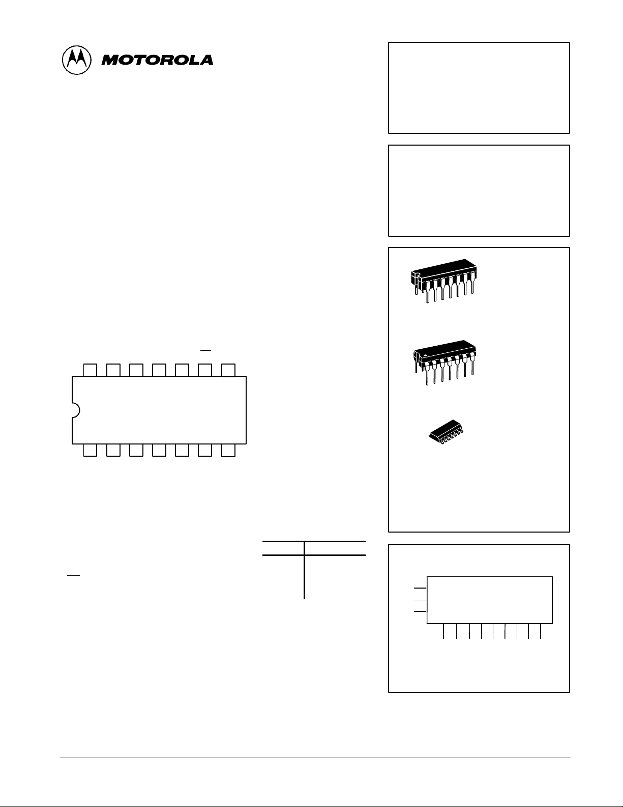
CONNECTION DIAGRAM DIP (TOP VIEW)
SN54/74LS164
SERIAL-IN PARALLEL-OUT
SHIFT REGISTER
LOW POWER SCHOTTKY
J SUFFIX
CERAMIC
14
1
CASE 632-08
VCCQ7Q6Q5Q4MR
14 13 12 11 10 9
123456
ABQ
PIN NAMES LOADING (Note a)
A, B
CP
MR
Q0–Q
NOTES:
a) 1 TTL Unit Load (U.L.) = 40 µA HIGH/1.6 mA LOW.
b) The Output LOW drive factor is 2.5 U.L. for Military (54) and 5 U.L. for Commercial (74)
T emperature Ranges.
Data Inputs
Clock (Active HIGH Going Edge) Input
Master Reset (Active LOW) Input
Outputs (Note b)
7
Q
0
Q
1
2
Q
3
CP
8
7
GND
NOTE:
The Flatpak version
has the same pinouts
(Connection Diagram) as
the Dual In-Line Package.
HIGH
0.5 U.L.
0.5 U.L.
0.5 U.L.
10 U.L.
LOW
0.25 U.L.
0.25 U.L.
0.25 U.L.
5 (2.5) U.L.
14
1
14
1
CASE 646-06
CASE 751A-02
ORDERING INFORMATION
SN54LSXXXJ Ceramic
SN74LSXXXN Plastic
SN74LSXXXD SOIC
LOGIC SYMBOL
1
A
2
B
8
CP
MR Q0Q1Q2Q3Q4Q5Q6Q
9 3 4 5 610111213
LS164
8-BIT SHIFT REGISTER
VCC = PIN 14
GND = PIN 7
N SUFFIX
PLASTIC
D SUFFIX
SOIC
7
FAST AND LS TTL DAT A
5-1
Page 2
SN54/74LS164
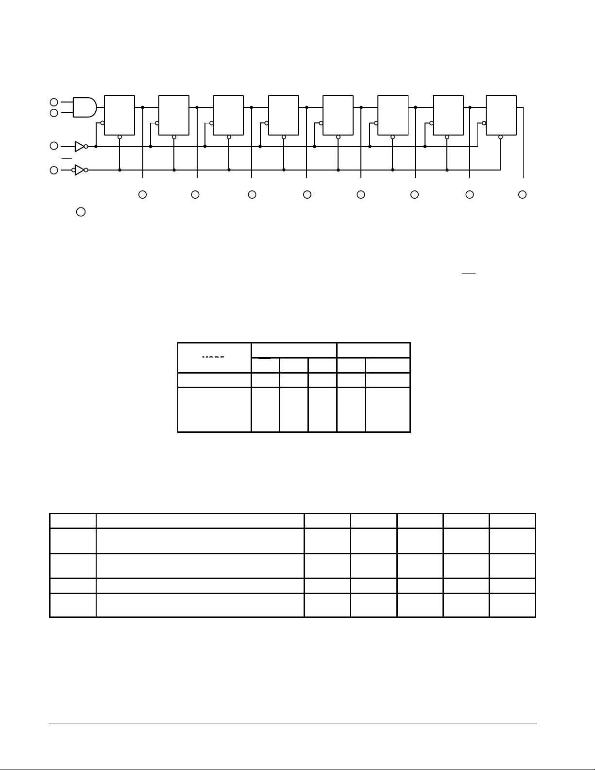
LOGIC DIAGRAM
A
1
2
B
CP
8
MR
9
DQ
C
VCC = PIN 14
GND = PIN 7
= PIN NUMBERS
D
DQ
Q
0
C
D
Q
1
DQ
C
D
FUNCTIONAL DESCRIPTION
The LS164 is an edge-triggered 8-bit shift register with serial data entry and an output from each of the eight stages. Data
is entered serially through one of two inputs (A or B); either of
these inputs can be used as an active HIGH Enable for data
entry through the other input. An unused input must be tied
HIGH, or both inputs connected together.
Q
2
DQ
Q
4
DQ
C
D
DQ
C
D
Q
C
D
3
63 4 5 11 1210 13
Q
5
DQ
C
D
Q
6
Each LOW-to-HIGH transition on the Clock (CP) input shifts
data one place to the right and enters into Q0 the logical AND
of the two data inputs (A•B) that existed before the rising clock
edge. A LOW level on the Master Reset (MR
) input overrides
all other inputs and clears the register asynchronously , forcing
all Q outputs LOW.
DQ
C
D
Q
7
MODE SELECT — TRUTH TABLE
OPERATING
MODE
Reset (Clear) L X X L L – L
Shift H I h L q0–q
L (l) = LOW Voltage Levels
H (h) = HIGH Voltage Levels
X = Don’t Care
qn = Lower case letters indicate the state of the referenced input or output one
qn = set-up time prior to the LOW to HIGH clock transition.
INPUTS OUTPUTS
MR A B Q
H I I L q0–q
H h I L q0–q
H h h H q0–q
Q1–Q
0
7
6
6
6
6
GUARANTEED OPERATING RANGES
Symbol Parameter Min Typ Max Unit
V
T
I
OH
I
OL
CC
A
Supply Voltage 54
74
Operating Ambient Temperature Range 54
74
Output Current — High 54, 74 –0.4 mA
Output Current — Low 54
74
4.5
4.75
–55
0
5.0
5.0
25
25
5.5
5.25
125
70
4.0
8.0
V
°C
mA
FAST AND LS TTL DATA
5-2
Page 3
SN54/74LS164
VILI
LOW Volt
V
pg
VOHOutput HIGH Volt
V
CC
,
OH
,
IN IH
VOLOutput LOW Volt
V
V
V
IIHI
HIGH C
t
C
L
pF
V
5.0 V
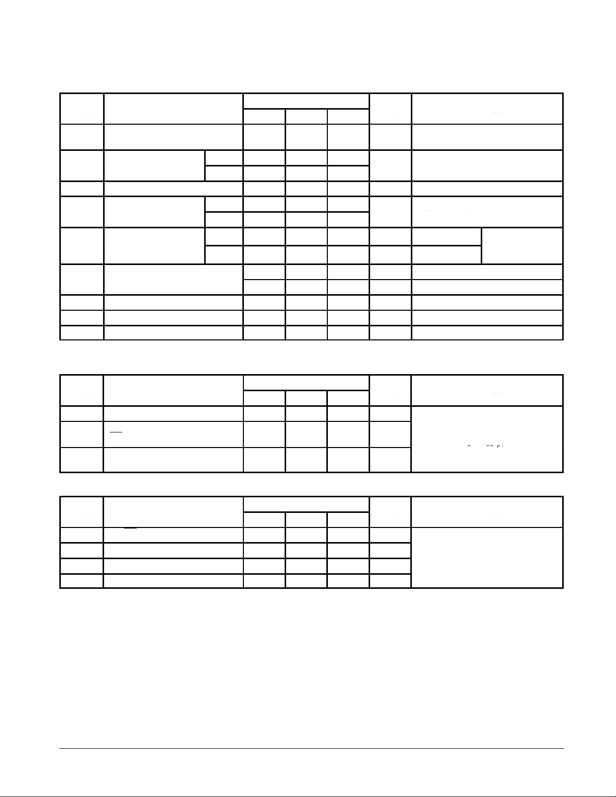
DC CHARACTERISTICS OVER OPERATING TEMPERATURE RANGE (unless otherwise specified)
Limits
Symbol Parameter
V
IH
V
IK
I
IL
I
OS
I
CC
Note 1: Not more than one output should be shorted at a time, nor for more than 1 second.
Input HIGH Voltage 2.0 V
nput
Input Clamp Diode Voltage –0.65 –1.5 V VCC = MIN, IIN = –18 mA
nput
Input LOW Current –0.4 mA VCC = MAX, VIN = 0.4 V
Short Circuit Current (Note 1) –20 –100 mA VCC = MAX
Power Supply Current 27 mA VCC = MAX
age
age
age
urren
54 0.7
74 0.8
54 2.5 3.5
74 2.7 3.5
54, 74 0.25 0.4 V IOL = 4.0 mA
74 0.35 0.5 V IOL = 8.0 mA
Min Typ Max
20 µA VCC = MAX, VIN = 2.7 V
0.1 mA VCC = MAX, VIN = 7.0 V
Unit Test Conditions
Guaranteed Input HIGH Voltage for
All Inputs
Guaranteed Input LOW Voltage for
All Inputs
VCC = MIN, IOH = MAX, VIN = V
or VIL per Truth Table
IH
VCC = VCC MIN,
=
IN
per Truth Table
or
IH
IL
AC CHARACTERISTICS (T
Symbol Parameter
f
MAX
t
PHL
t
PLH
t
PHL
Maximum Clock Frequency 25 36
Propagation Delay
MR to Output Q
Propagation Delay
Clock to Output Q
= 25°C)
A
AC SETUP REQUIREMENTS (T
Symbol Parameter
t
t
t
t
W
s
h
rec
CP, MR Pulse Width 20
Data Setup Time 15
Data Hold Time 5.0
MR to Clock Recovery Time 20
= 25°C)
A
Limits
Min Typ Max
24 36 ns
17
21
Limits
Min Typ Max
27
32
Unit Test Conditions
MHz
VCC = 5.0 V
C
= 15 pF
= 15
ns
Unit Test Conditions
ns
ns
ns
ns
CC
=
FAST AND LS TTL DATA
5-3
Page 4
CP
Q
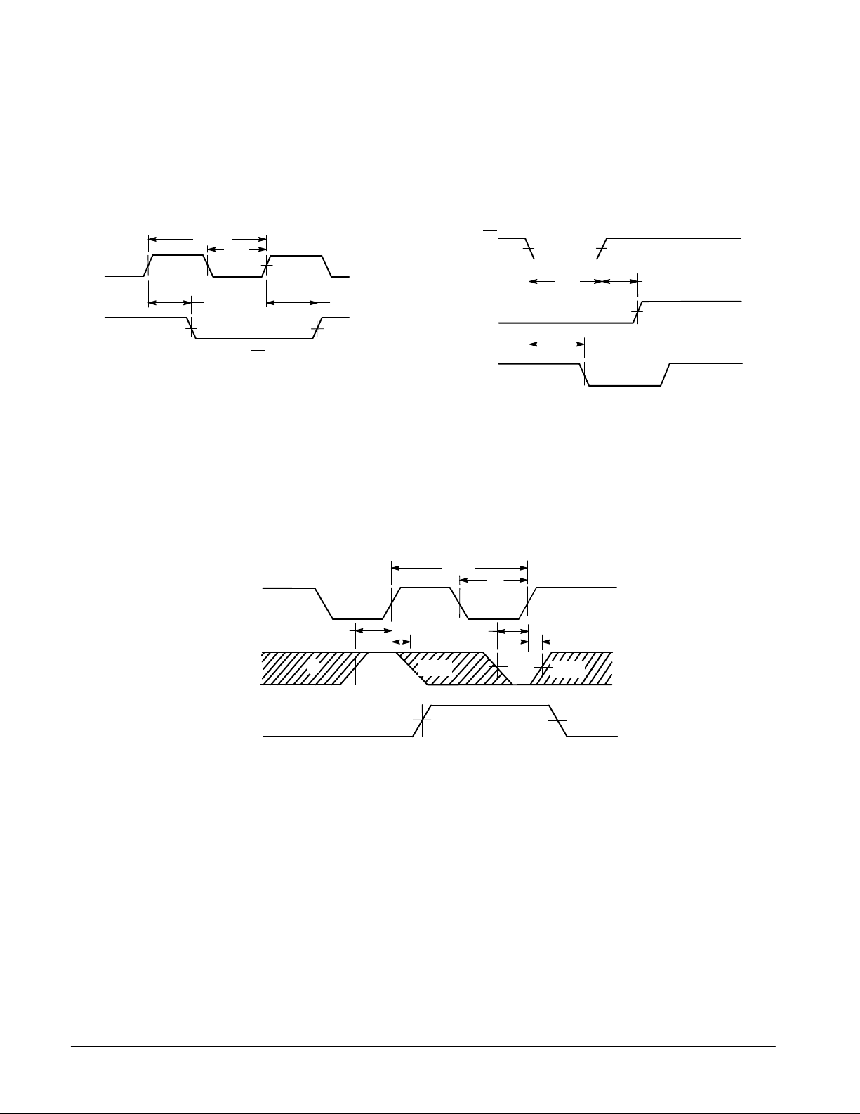
*The shaded areas indicate when the input is permitted to change for predictable output performance.
I
/f
max
t
1.3 V 1.3 V
t
PHL
1.3 V
CONDITIONS: MR = H
SN54/74LS164
AC WAVEFORMS
MR
W
1.3 V
t
PLH
1.3 V
CP
Q
1.3 V
t
W
t
PHL
1.3 V
1.3 V
t
rec
1.3 V
Figure 1. Clock to Output Delays
and Clock Pulse Width
CP
D
Q
Figure 2. Master Reset Pulse Width,
Master Reset to Output Delay and
Master Reset to Clock Recovery Time
1/f
max
t
W
1.3 V
ts(H)
1.3 V
1.3 V
th(H)
1.3 V
1.3 V
1.3 V 1.3 V
ts(L)
1.3V
Figure 3. Data Setup and Hold Times
th(L)
1.3 V*
1.3 V
FAST AND LS TTL DATA
5-4
 Loading...