

Page 1
SN54/74LS147
10-LINE-TO-4-LINE
AND 8-LINE-TO-3-LINE
PRIORITY ENCODERS
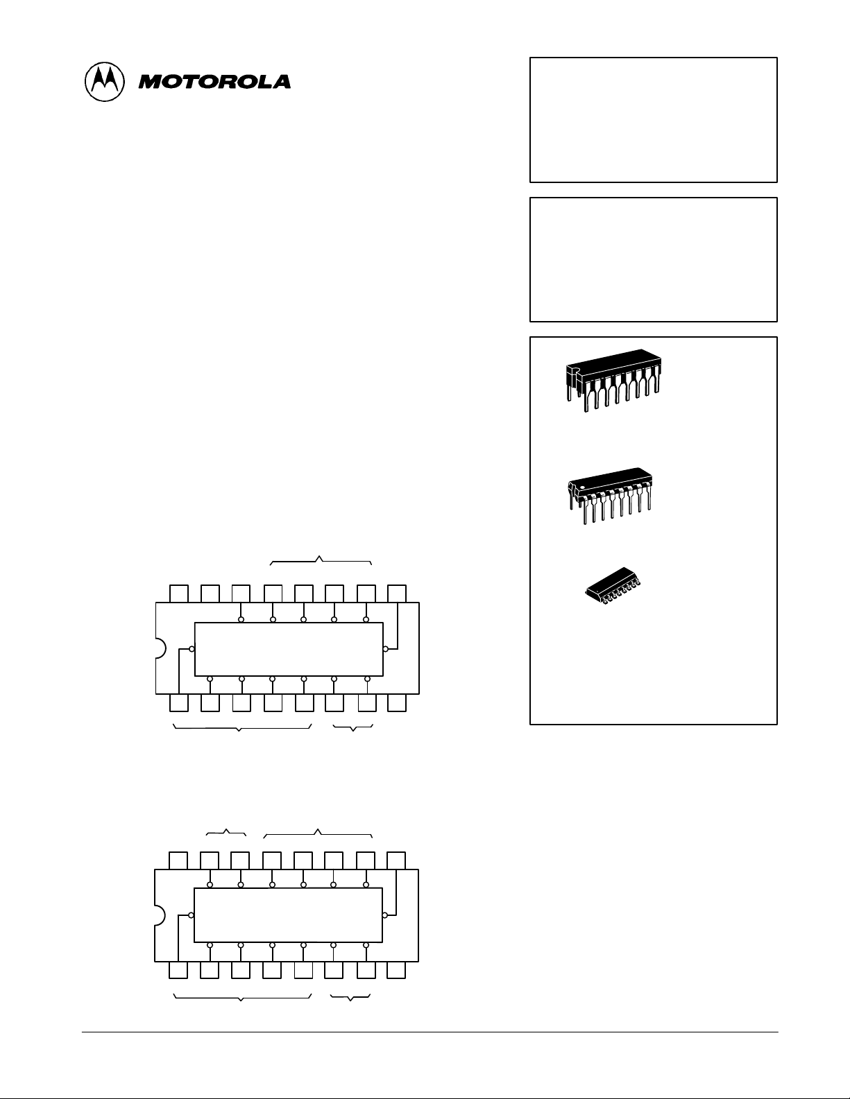
The SN54/74LS147 and the SN54/74LS148 are Priority Encoders. They
provide priority decoding of the inputs to ensure that only the highest order
data line is encoded. Both devices have data inputs and outputs which are
active at the low logic level.
The LS147 encodes nine data lines to four-line (8-4-2-1) BCD. The implied
decimal zero condition does not require an input condition because zero is
encoded when all nine data lines are at a high logic level.
The LS148 encodes eight data lines to three-line (4-2-1) binary (octal). By
providing cascading circuitry (Enable Input EI and Enable Output EO) octal
expansion is allowed without needing external circuitry .
The SN54/74LS748 is a proprietary Motorola part incorporating a built-in
deglitcher network which minimizes glitches on the GS output. The glitch
occurs on the negative going transition of the EI input when data inputs 0–7
are at logical ones.
The only dc parameter differences between the LS148 and the LS748 are
that (1) Pin 10 (input 0) has a fan-in of 2 on the LS748 versus a fan-in of 1 on
the LS148; (2) Pins 1, 2, 3, 4, 1 1, 12 and 13 (inputs 1, 2, 3, 4, 5, 6, 7) have a
fan-in of 3 on the LS748 versus a fan-in of 2 on the LS148.
The only ac difference is that t
45 ns.
SN54 /74LS147
OUTPUT INPUTS OUTPUT
from EI to EO is changed from 40 to
PHL
(TOP VIEW)
SN54/74LS148
SN54/74LS748
10-LINE-TO-4-LINE
AND 8-LINE-TO-3-LINE
PRIORITY ENCODERS
LOW POWER SCHOTTKY
J SUFFIX
CERAMIC
16
1
16
1
CASE 620-09
N SUFFIX
PLASTIC
CASE 648-08
D3219AVCCNC
16 15
123456
45678CBGND
VCCEO GS 3 2 1 0 A0
16 15
123456
4 5 6 7 E1 A2 A1 GND
14 13 12 11 10 9
D3219
A4
5678CB
7
INPUTS OUTPUTS
SN54/74LS148
SN54/74LS748
(TOP VIEW)
OUTPUTS
14 13 12 11 10 9
EO GS 3 2 1 0
567EIA2A1
INPUTS OUTPUTS
INPUTS OUTPUT
A04
7
8
8
D SUFFIX
16
1
ORDERING INFORMATION
SN54LSXXXJ Ceramic
SN74LSXXXN Plastic
SN74LSXXXD SOIC
SOIC
CASE 751B-03
FAST AND LS TTL DAT A
5-1
Page 2
SN54/74LS147 • SN54/74LS148 • SN54/74LS748
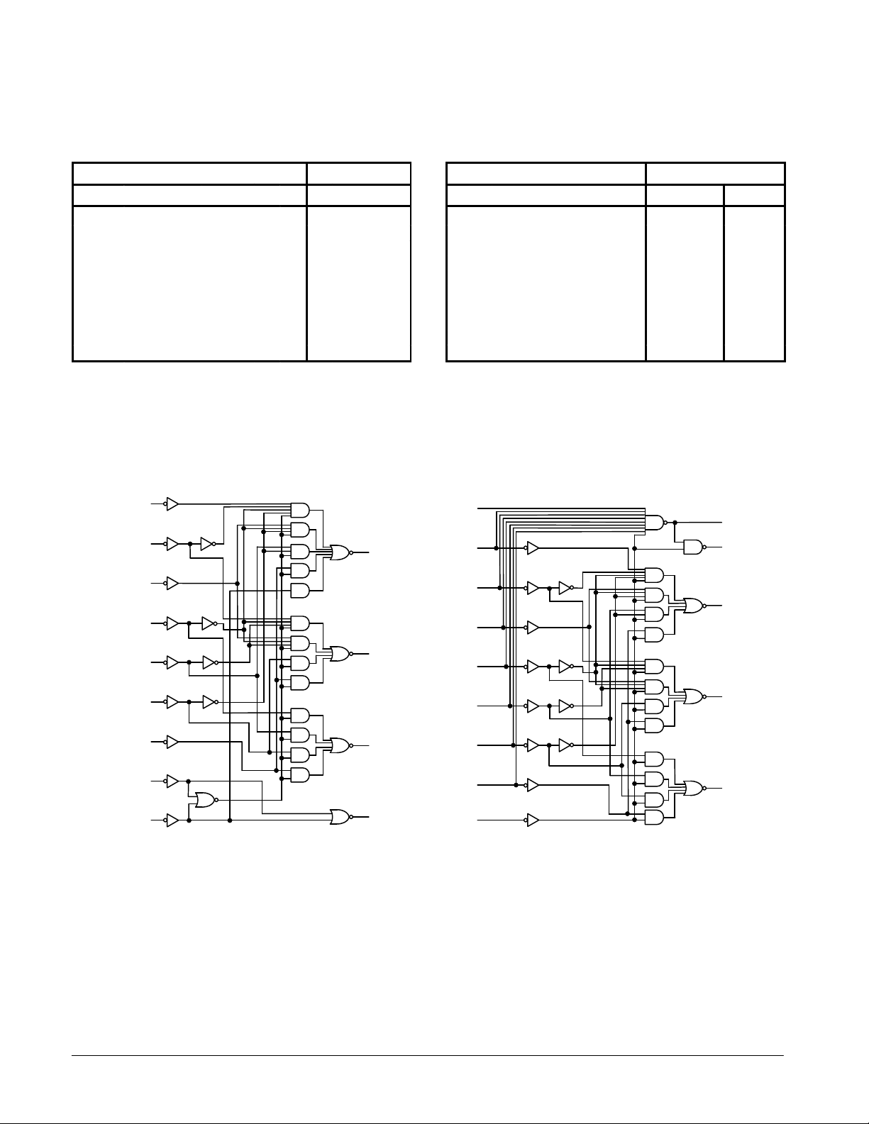
SN54/74LS147
FUNCTION TABLE
INPUTS OUTPUTS
1 2 3 4 5 6 7 8 9 D C B A
H H H H H H H H H H H H H
X XXXXXXXLLHHL
XXXXXXXLHLHHH
XXXXXXLHHHLLL
XXXXXLHHHHLLH
XX XXL HHHHHLHL
XXXLHHHHHHLHH
XX LHHHHHHHHLL
XLHHHHHHHHHLH
LHHHHHHHHHHHL
H = HIGH Logic Level, L = LOW Logic Level, X = Irrelevant
FUNCTIONAL BLOCK DIAGRAMS
SN54/74LS148
SN54/74LS748
FUNCTION TABLE
INPUTS OUTPUTS
EI 0 1 2 3 4 5 6 7 A2 A1 A0 GS EO
H X X X X X X X X H H H H H
L HHHHHHHH H HHH L
LXXXXXXXL L LL L H
LXXXXXXLH L LH L H
LXXXXXLHHL HL L H
LXXXXLHHHL HH L H
LXXXLHHHH H LL L H
LXXLHHHHHH LH L H
LX LHHHHHHH HL L H
LLHHHHHHHHHH L H
(11)
1
(12)
2
(13)
3
(1)
4
(2)
5
(3)
6
(4)
7
(5)
8
(10)
9
(9)
(7)
(6)
(14)
A
B
C
D
(10)
0
(11)
1
(12)
2
(13)
3
(1)
4
(2)
5
(3)
6
(4)
7
(5)
EI
(15)
(14)
(8)
(7)
(6)
EO
GS
A0
A1
A2
SN54/74LS147 SN54/74LS148
FAST AND LS TTL DATA
5-2
Page 3
SN54/74LS147 • SN54/74LS148 • SN54/74LS748
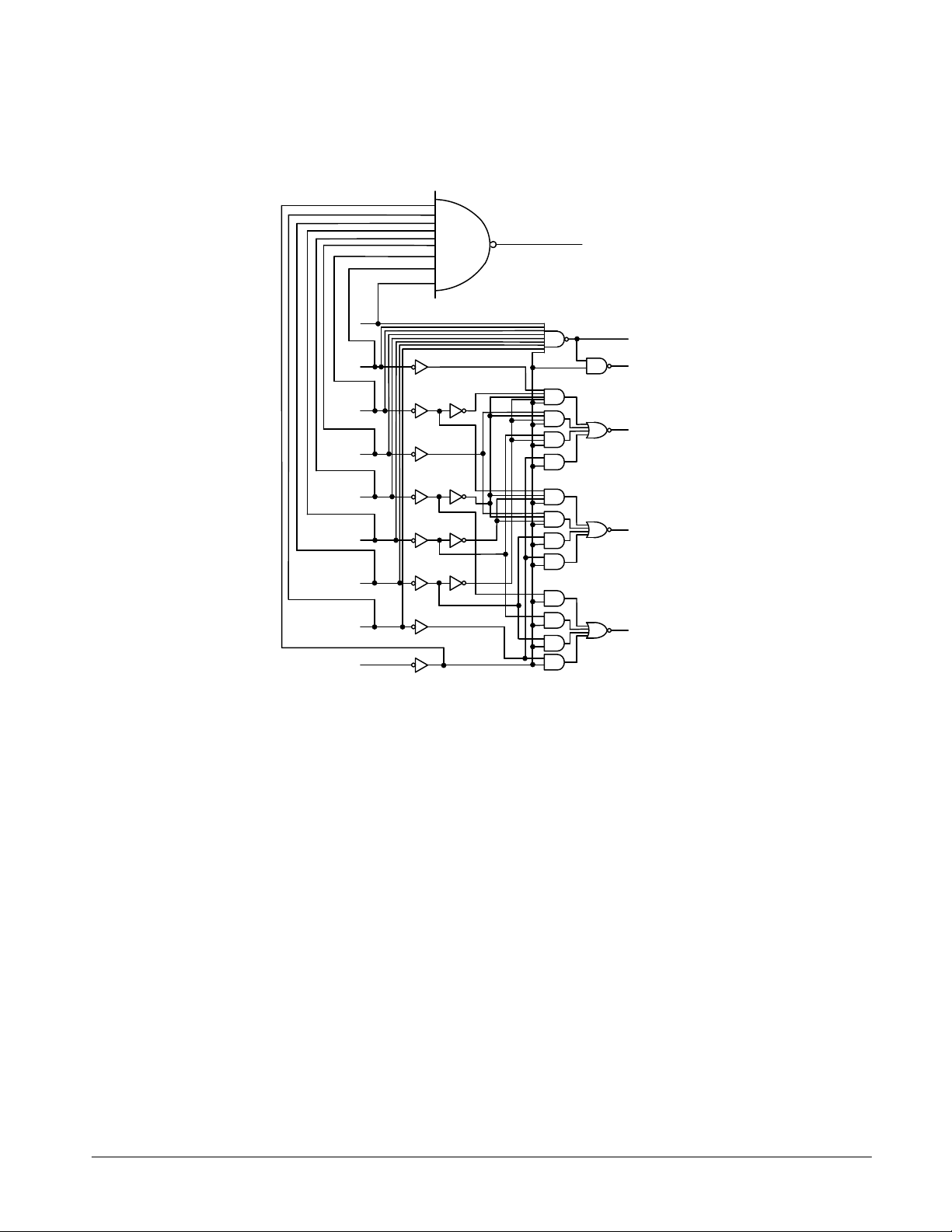
FUNCTIONAL BLOCK DIAGRAMS (continued)
G31
(10)
EI
0
(11)
1
(12)
2
(13)
3
4
5
6
7
(1)
(2)
(3)
(4)
(5)
G2
G9
G3
G4
G10
G5
G11
G6
G12
G7
G8
G1
G13
G29
G18
G23
G28
(15)
(14)
(9)
(7)
(6)
EO
GS
A0
A1
A2
SN54/74LS748
FAST AND LS TTL DATA
5-3
Page 4
SN54/74LS147 • SN54/74LS148 • SN54/74LS748
VILI
LOW Volt
V
pg
VOHOutput HIGH Volt
CC
,
OH
,
IN IH
VOLOutput LOW Volt
V
V
V
I
IH
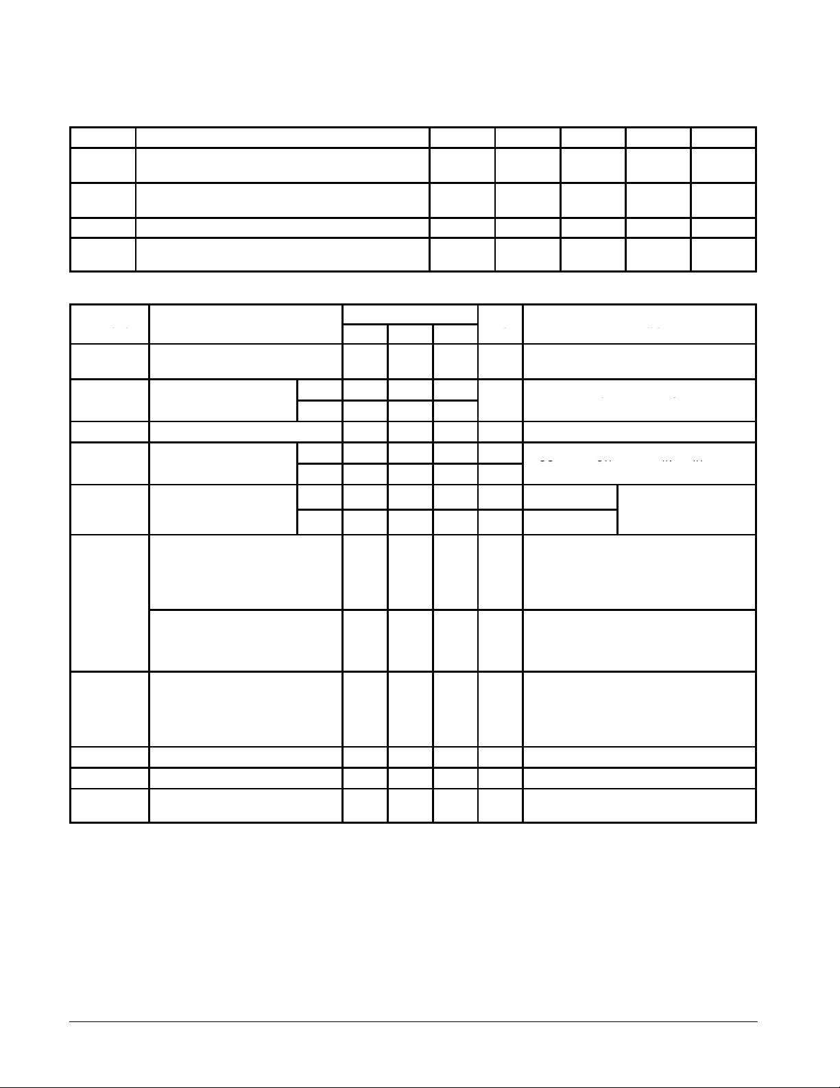
GUARANTEED OPERATING RANGES
Symbol Parameter Min Typ Max Unit
V
CC
T
A
I
OH
I
OL
DC CHARACTERISTICS OVER OPERATING TEMPERATURE RANGE (unless otherwise specified)
Symbol Parameter
V
IH
V
IK
I
IH
I
IL
I
OS
I
CCH
I
CCL
Note 1: Not more than one output should be shorted at a time, nor for more than 1 second.
Supply Voltage 54
Operating Ambient Temperature Range 54
Output Current — High 54, 74 –0.4 mA
Output Current — Low 54
Limits
Min Typ Max
Input HIGH Voltage 2.0 V
nput
Input Clamp Diode Voltage –0.65 –1.5 V VCC = MIN, IIN = –18 mA
Input HIGH Current
All Others
Input 0 (LS748)
Inputs 1–7 (LS148)
Inputs 1–7 (LS748)
All Others
Input 0 (LS748)
Inputs 1–7 (LS148)
Inputs 1–7 (LS748)
Input LOW Current
All Others
Input 0 (LS748)
Inputs 1–7 (LS148)
Inputs 1–7 (LS748)
Short Circuit Current (Note 1) –20 –100 mA VCC = MAX
Power Supply Current Output HIGH 17 mA VCC = MAX, All Inputs = 4.5 V
Output LOW 20 mA
age
age
age
54 0.7
74 0.8
54 2.5 3.5 V
74 2.7 3.5 V
54, 74 0.25 0.4 V IOL = 4.0 mA
74 0.35 0.5 V IOL = 8.0 mA
74
74
74
20
40
40
60
0.1
0.2
0.2
0.3
–0.4
–0.8
–0.8
–1.2
4.5
4.75
–55
0
Unit Test Conditions
Guaranteed Input HIGH Voltage for
All Inputs
Guaranteed Input LOW Voltage for
All Inputs
VCC = MIN, IOH = MAX, VIN = V
or VIL per Truth Table
µA VCC = MAX, VIN = 2.7 V
mA VCC = MAX, VIN = 7.0 V
mA VCC = MAX, VIN = 0.4 V
VCC = MAX, Inputs 7 & E1 = GND
All Other Inputs = 4.5 V
5.0
5.0
25
25
5.5
5.25
125
70
4.0
8.0
VCC = VCC MIN,
=
IN
IL
per Truth Table
or
IH
IH
V
°C
mA
FAST AND LS TTL DATA
5-4
Page 5
SN54/74LS147 • SN54/74LS148 • SN54/74LS748
From
To
AnyA
p
L
p,
AnyA
p
From
To
1 th
7
A0, A1
A2
p
1 th
7
A0, A1
A2
p
0 th
7
EO
p
0 th
7
GS
p
R
L
kΩ
EI
A0, A1
A2
p
EI
GS
p
I
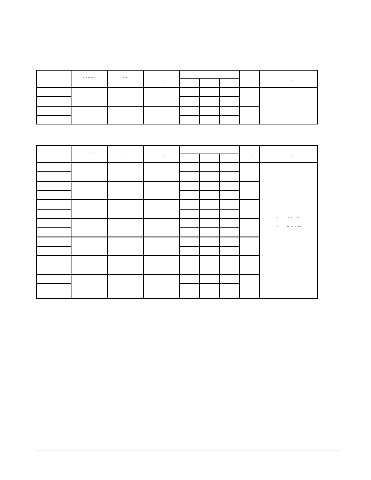
AC CHARACTERISTICS (V
SN54/74LS147
From To
Symbol
t
PLH
t
PHL
t
PLH
t
PHL
(Input)
SN54/74LS148
SN54/74LS748
From To
Symbol
t
PLH
t
PHL
t
PLH
t
PHL
t
PLH
t
PHL
t
PLH
t
PHL
t
PLH
t
PHL
t
PLH
t
PHL
t
PLH
t
PHL
(Input)
ru
ru
ru
ru
EI EO
= 5.0 V, TA = 25°C)
CC
(Output)
ny
ny
(Output)
, or
, or
, or
Waveform
In-phase
output
Out-of-phase
output
Waveform
In-phase
output
Out-of-phase
output
Out-of-phase
output
In-phase
output
In-phase
output
In-phase
output
n-phase
output
Limits
Min Typ Max
12 18
12 18
21 33
15 23
Limits
Min Typ Max
14 18
15 25
20 36
16 29
7.0 18
25 40
35 55
9.0 21
16 25
12 25
12 17
14 36
12 21
28
30
40
45
Unit Test Conditions
ns
ns
Unit Test Conditions
ns
ns
ns
ns
ns
ns
ns
RL = 2.0 kΩ
R
(LS148)
(LS748)
CL = 15 pF,
CL = 15 pF,
= 2.0 kΩ
= 2.0
FAST AND LS TTL DATA
5-5
 Loading...