

Page 1
DUAL 1-OF-4 DECODER/
DEMULTIPLEXER
The LSTTL/MSI SN54/74LS139 is a high speed Dual 1-of-4 Decoder/Demultiplexer. The device has two independent decoders, each accepting two
inputs and providing four mutually exclusive active LOW Outputs. Each
decoder has an active LOW Enable input which can be used as a data input
for a 4-output demultiplexer. Each half of the LS139 can be used as a function
generator providing all four minterms of two variables. The LS139 is
fabricated with the Schottky barrier diode process for high speed and is
completely compatible with all Motorola TTL families.
• Schottky Process for High Speed
• Multifunction Capability
• Two Completely Independent 1-of-4 Decoders
• Active Low Mutually Exclusive Outputs
• Input Clamp Diodes Limit High Speed Termination Effects
• ESD > 3500 Volts
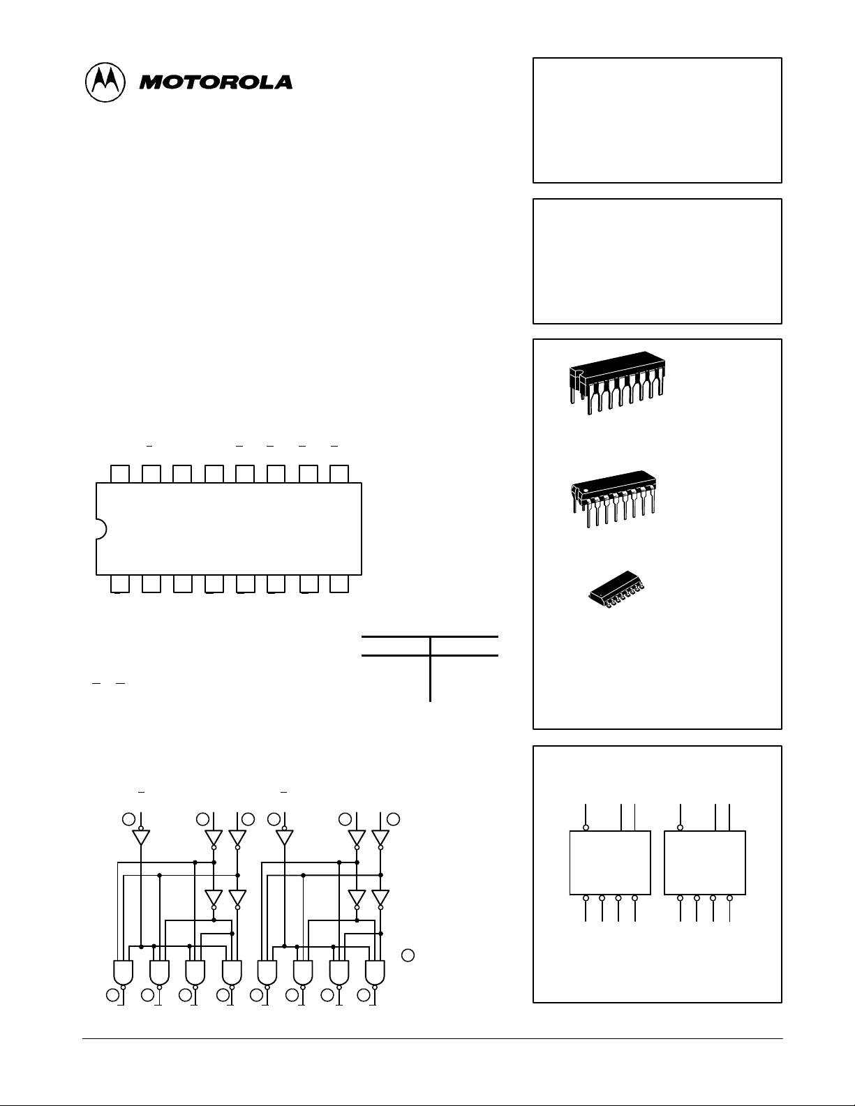
CONNECTION DIAGRAM DIP (TOP VIEW)
V
CC
16 15
E
bAObA1bO0b
14 13 12 11 10 9
O
O
1b
2b
O
3b
NOTE:
The Flatpak version
has the same pinouts
(Connection Diagram) as
the Dual In-Line Package.
SN54/74LS139
DUAL 1-OF-4 DECODER/
DEMULTIPLEXER
LOW POWER SCHOTTKY
J SUFFIX
CERAMIC
16
1
16
1
CASE 620-09
N SUFFIX
PLASTIC
CASE 648-08
123456
E
A0aA1aO
a
PIN NAMES LOADING (Note a)
A0, A
1
E
O
0–O3
NOTES:
a) 1 TTL Unit Load (U.L.) = 40 µA HIGH/1.6 mA LOW.
b) The Output LOW drive factor is 2.5 U.L. for Military (54) and 5 U.L. for Commercial (74)
T emperature Ranges.
0aO1aO2aO3a
Address Inputs
Enable (Active LOW) Input
Active LOW Outputs (Note b)
7
GND
8
HIGH
0.5 U.L.
0.5 U.L.
10 U.L.
LOW
0.25 U.L.
0.25 U.L.
5 (2.5) U.L.
LOGIC DIAGRAM
E
a
12
546 910
O
O1aO
0a
A0aA
1a
7
O
3aO0bO1bO2bO3b
2a
E
b
3
1112
A
A
0b
1b
14
1315
VCC = PIN 16
GND = PIN 8
= PIN NUMBERS
D SUFFIX
16
1
SOIC
CASE 751B-03
ORDERING INFORMATION
SN54LSXXXJ Ceramic
SN74LSXXXN Plastic
SN74LSXXXD SOIC
LOGIC SYMBOL
123 151413
EA
DECODER a DECODER b
O0O1O2O
4 5 6 7 12 11 10 9
A
0
VCC = PIN 16
GND = PIN 8
1
3
EA
O0O2O
O
1
A
0
1
3
FAST AND LS TTL DAT A
5-1
Page 2
SN54/74LS139
FUNCTIONAL DESCRIPTION
The LS139 is a high speed dual 1-of-4 decoder/demultiplexer fabricated with the Schottky barrier diode process. The
device has two independent decoders, each of which accept
two binary weighted inputs (A0, A1) and provide four mutually
exclusive active LOW outputs (O
active LOW Enable (E
). When E is HIGH all outputs are forced
HIGH. The enable can be used as the data input for a 4-output
). Each decoder has an
0–O3
demultiplexer application.
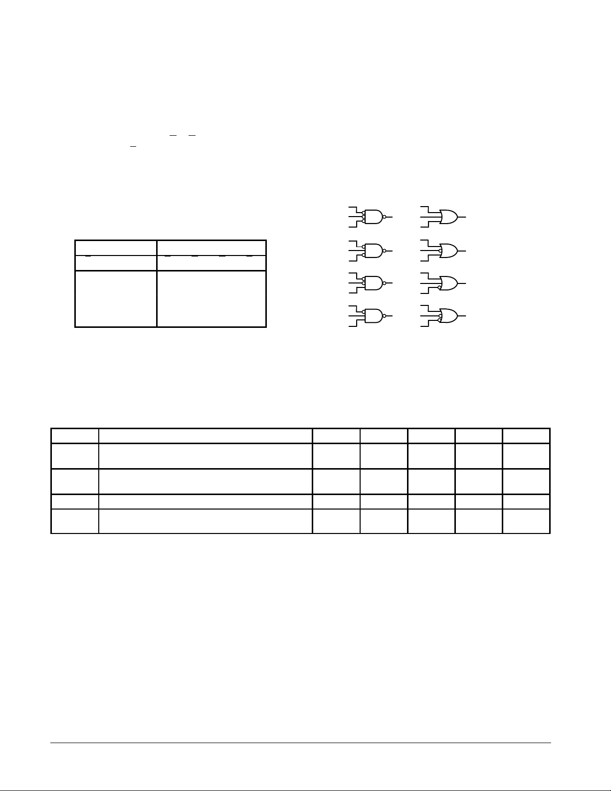
Each half of the LS139 generates all four minterms of two
variables. These four minterms are useful in some applications, replacing multiple gate functions as shown in Fig. a, and
thereby reducing the number of packages required in a logic
network.
E
A
0
O
0
A
1
E
A
O
0
1
A
1
E
A
O
0
2
A
1
E
A
O
0
3
A
1
Figure a
O
0
O
1
O
2
O
3
TRUTH TABLE
INPUTS OUTPUTS
E A
H X X H H H H
L LLLHHH
LHLHLHH
LLHHHLH
LHHHHHL
H = HIGH Voltage Level
L = LOW Voltage Level
X = Don’t Care
A
O
O
O
0
1
0
1
O
2
E
A
0
A
1
E
A
0
A
3
1
E
A
0
A
1
E
A
0
A
1
GUARANTEED OPERATING RANGES
Symbol Parameter Min Typ Max Unit
V
T
I
OH
I
OL
CC
A
Supply Voltage 54
74
Operating Ambient Temperature Range 54
74
Output Current — High 54, 74 –0.4 mA
Output Current — Low 54
74
4.5
4.75
–55
0
5.0
5.0
25
25
5.5
5.25
125
70
4.0
8.0
V
°C
mA
FAST AND LS TTL DATA
5-2
Page 3
SN54/74LS139
VILI
LOW Volt
V
pg
54
2.5
3.5
V
VOHOutput HIGH Voltage
CC
,
OH
,
IN IH
VOLOutput LOW Volt
V
V
V
IIHI
HIGH C
t
Levels of
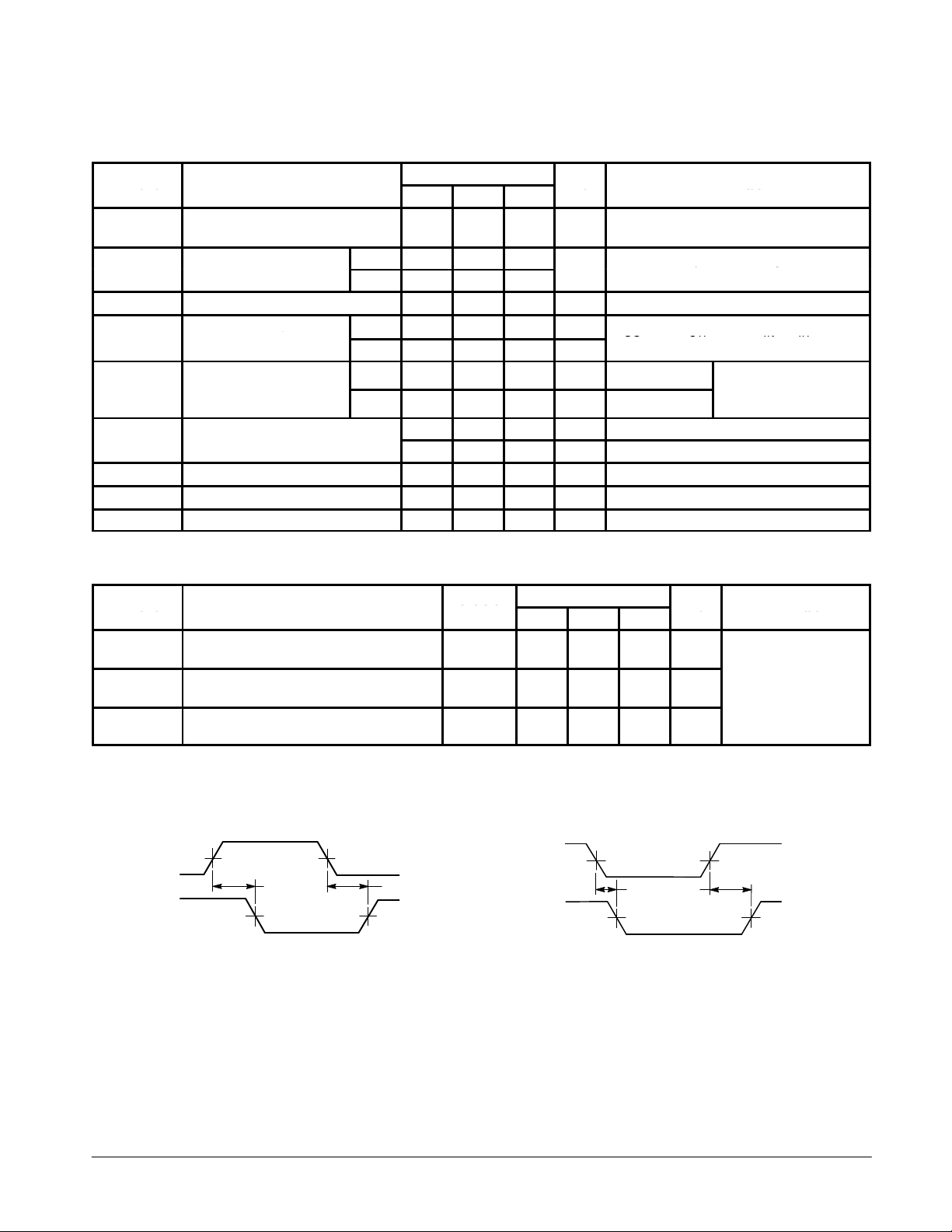
DC CHARACTERISTICS OVER OPERATING TEMPERATURE RANGE (unless otherwise specified)
Limits
Symbol Parameter
V
IH
V
IK
I
IL
I
OS
I
CC
Note 1: Not more than one output should be shorted at a time, nor for more than 1 second.
Input HIGH Voltage 2.0 V
nput
Input Clamp Diode Voltage –0.65 –1.5 V VCC = MIN, IIN = –18 mA
nput
Input LOW Current –0.4 mA VCC = MAX, VIN = 0.4 V
Short Circuit Current (Note 1) –20 –100 mA VCC = MAX
Power Supply Current 11 mA VCC = MAX
age
age
urren
54 0.7
74 0.8
74 2.7 3.5 V
54, 74 0.25 0.4 V IOL = 4.0 mA
74 0.35 0.5 V IOL = 8.0 mA
Min Typ Max
0.1 mA VCC = MAX, VIN = 7.0 V
Unit Test Conditions
Guaranteed Input HIGH Voltage for
All Inputs
Guaranteed Input LOW Voltage for
All Inputs
VCC = MIN, IOH = MAX, VIN = V
or VIL per Truth Table
20 µA VCC = MAX, VIN = 2.7 V
IH
VCC = VCC MIN,
=
or
IN
IL
per Truth Table
IH
AC CHARACTERISTICS (T
Symbol Parameter
t
PLH
t
PHL
t
PLH
t
PHL
t
PLH
t
PHL
Propagation Delay
Address to Output
Propagation Delay
Address to Output
Propagation Delay
Enable to Output
IN
OUT
1.3 V
V
V
= 25°C)
A
t
PHL
1.3 V
Figure 1 Figure 2
1.3 V
AC WAVEFORMS
t
PLH
1.3 V
Levels of
Delay
2
2
3
3
2
2
Limits
Min Typ Max
V
IN
V
OUT
13
22
18
25
16
21
1.3 V
20
33
29
38
24
32
t
PHL
1.3 V
Unit Test Conditions
ns
VCC = 5.0 V
CL = 15 pF
1.3 V
1.3 V
t
PLH
ns
ns
FAST AND LS TTL DATA
5-3
 Loading...