

Page 1
OPERATION
SN54HCT645, SN74HCT645
OCTAL BUS TRANSCEIVERS
WITH 3-STATE OUTPUTS
SCLS019B – MARCH 1984 – REVISED MA Y 1997
D
Inputs Are TTL-Voltage Compatible
D
True Logic
D
High-Current 3-State Outputs Can Drive up
to 15 LSTTL Loads
D
Package Options Include Plastic
Small-Outline (DW) and Ceramic Flat (W)
Packages, Ceramic Chip Carriers (FK), and
Standard Plastic (N) and Ceramic (J)
300-mil DIPs
description
These octal bus transceivers are designed for
asynchronous two-way communication between
data buses. These devices transmit data from the
A bus to the B bus or from the B bus to the A bus,
depending upon the level at the direction-control
(DIR) input. The output-enable (OE
used to disable the device so the buses are
effectively isolated.
The SN54HCT645 is characterized for operation
over the full military temperature range of –55°C
to 125°C. The SN74HCT645 is characterized for
operation from –40°C to 85°C.
FUNCTION TABLE
INPUTS
OE DIR
L L B data to A bus
L H A data to B bus
H X Isolation
) input can be
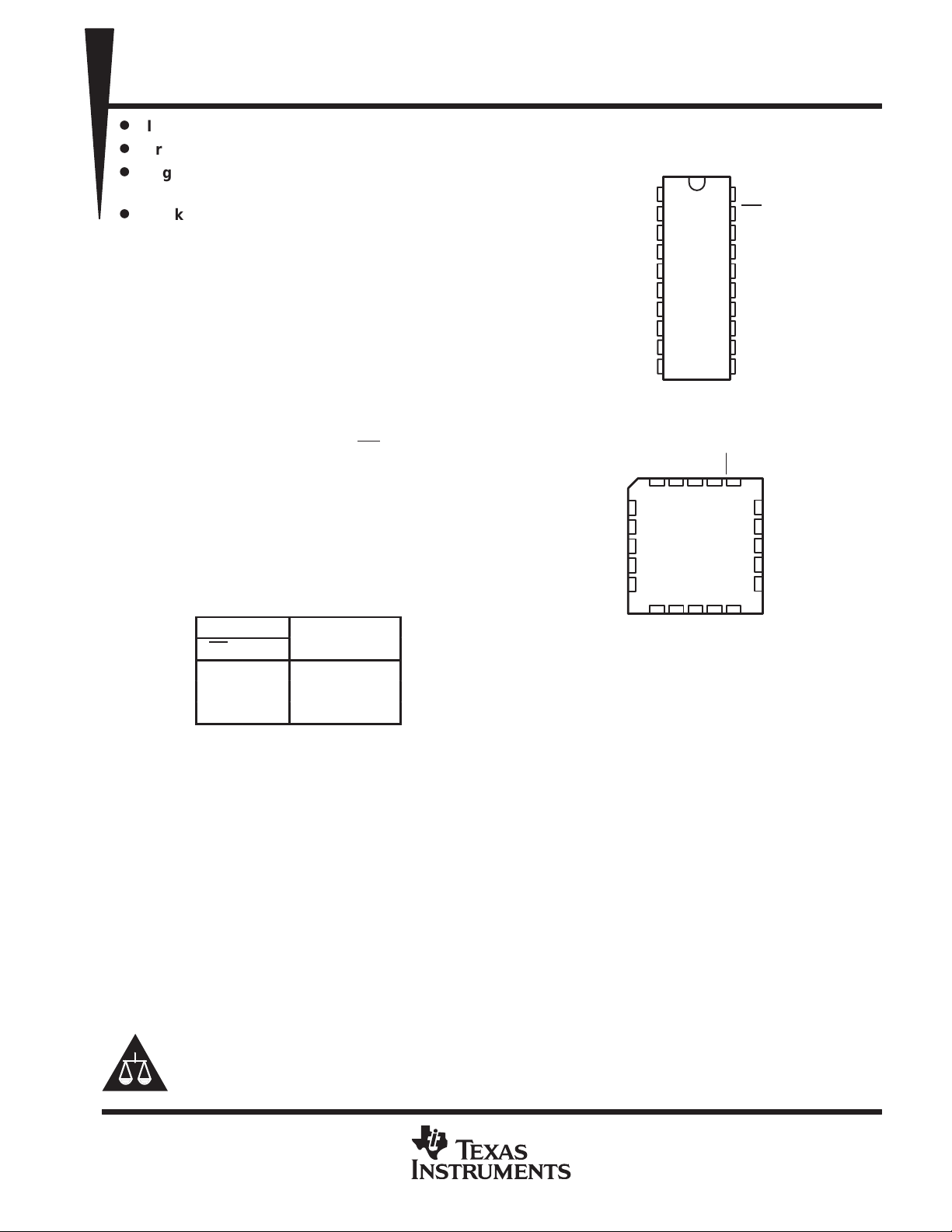
SN54HCT645 ...J OR W PACKAGE
SN74HCT645 . . . DW OR N PACKAGE
SN54HCT645 . . . FK PACKAGE
A3
A4
A5
A6
A7
(TOP VIEW)
1
DIR
2
A1
3
A2
4
A3
5
A4
6
A5
7
A6
8
A7
9
A8
10
GND
(TOP VIEW)
A2A1DIR
3212019
4
5
6
7
8
10 11 12 13
9
A8
B8
20
19
18
17
16
15
14
13
12
11
V
CC
B7
V
OE
B1
B2
B3
B4
B5
B6
B7
B8
OE
18
17
16
15
14
B6
CC
B1
B2
B3
B4
B5
GND
Please be aware that an important notice concerning availability, standard warranty, and use in critical applications of
Texas Instruments semiconductor products and disclaimers thereto appears at the end of this data sheet.
UNLESS OTHERWISE NOTED this document contains PRODUCTION
DATA information current as of publication date. Products conform to
specifications per the terms of Texas Instruments standard warranty.
Production processing does not necessarily include testing of all
parameters.
POST OFFICE BOX 655303 • DALLAS, TEXAS 75265
Copyright 1997, Texas Instruments Incorporated
1
Page 2
SN54HCT645, SN74HCT645
OCTAL BUS TRANSCEIVERS
WITH 3-STATE OUTPUTS
SCLS019B – MARCH 1984 – REVISED MA Y 1997
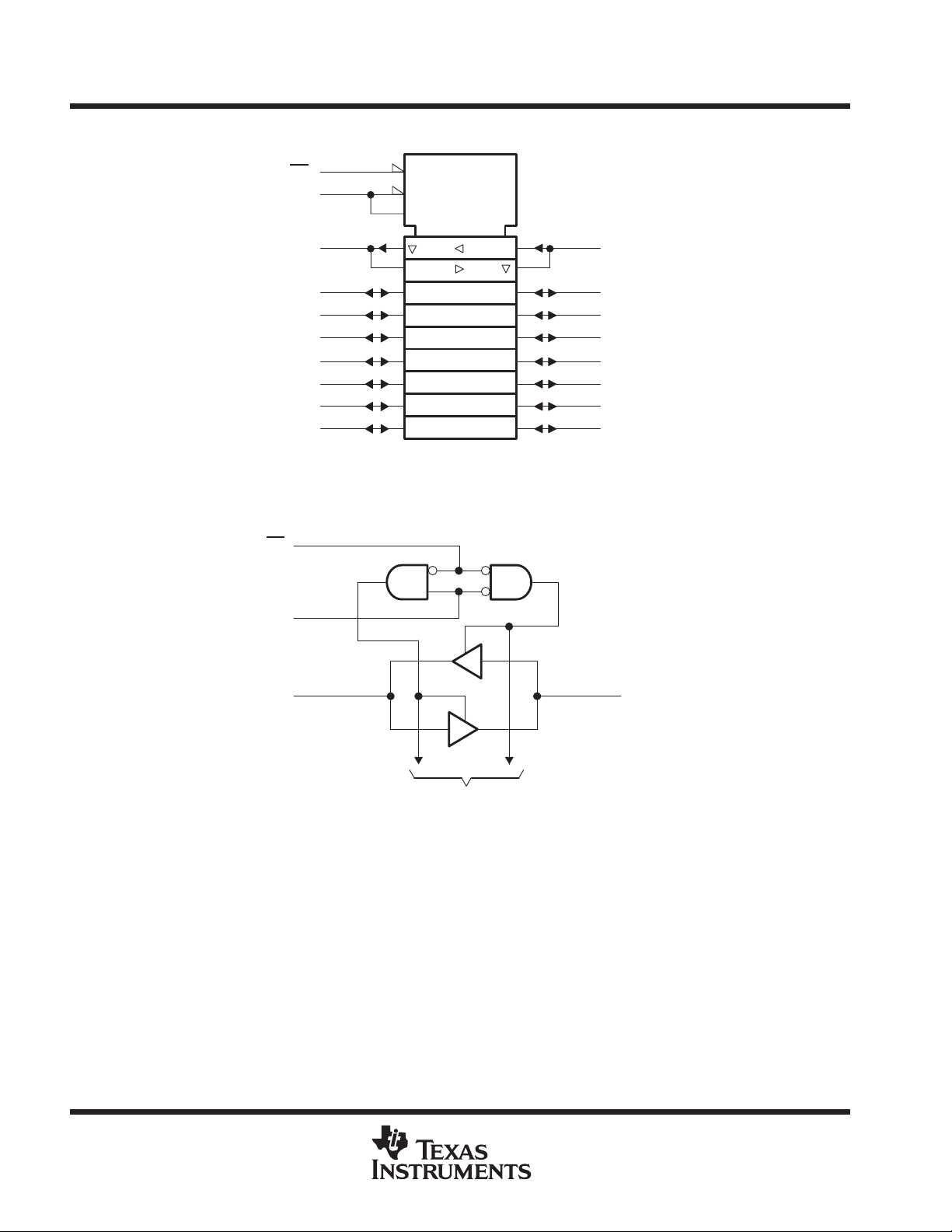
logic symbol
†
This symbol is in accordance with ANSI/IEEE Std 91-1984 and IEC Publication 617-12.
†
OE
DIR
A1
A2
A3
A4
A5
A6
A7
A8
19
1
2
3
4
5
6
7
8
9
G3
3 EN1 [BA]
3 EN2 [AB]
1
2
logic diagram (positive logic)
19
OE
18
17
16
15
14
13
12
11
B1
B2
B3
B4
B5
B6
B7
B8
1
DIR
218
A1
To Seven Other Transceivers
B1
2
POST OFFICE BOX 655303 • DALLAS, TEXAS 75265
Page 3
UNIT
PARAMETER
TEST CONDITIONS
V
UNIT
VOHV
V
V
4.5 V
V
VOLV
V
V
4.5 V
V
SN54HCT645, SN74HCT645
OCTAL BUS TRANSCEIVERS
WITH 3-STATE OUTPUTS
SCLS019B – MARCH 1984 – REVISED MA Y 1997
absolute maximum ratings over operating free-air temperature range
Supply voltage range, V
–0.5 V to 7 V. . . . . . . . . . . . . . . . . . . . . . . . . . . . . . . . . . . . . . . . . . . . . . . . . . . . . . . . . .
CC
†
Input clamp current, IIK (VI < 0 or VI > VCC) (see Note 1) ±20 mA. . . . . . . . . . . . . . . . . . . . . . . . . . . . . . . . . . . .
Output clamp current, IOK (VO < 0 or VO > VCC) (see Note 1) ±20 mA. . . . . . . . . . . . . . . . . . . . . . . . . . . . . . . .
Continuous output current, IO (VO = 0 to VCC) ±35 mA. . . . . . . . . . . . . . . . . . . . . . . . . . . . . . . . . . . . . . . . . . . . . .
Continuous current through VCC or GND ±70 mA. . . . . . . . . . . . . . . . . . . . . . . . . . . . . . . . . . . . . . . . . . . . . . . . . . .
Package thermal impedance, θ
(see Note 2): DW package 97°C/W. . . . . . . . . . . . . . . . . . . . . . . . . . . . . . . . .
JA
N package 67°C/W. . . . . . . . . . . . . . . . . . . . . . . . . . . . . . . . . . .
Storage temperature range, T
†
Stresses beyond those listed under “absolute maximum ratings” may cause permanent damage to the device. These are stress ratings only, and
functional operation of the device at these or any other conditions beyond those indicated under “recommended operating conditions” is not
implied. Exposure to absolute-maximum-rated conditions for extended periods may affect device reliability.
NOTES: 1. The input and output voltage ratings may be exceeded if the input and output current ratings are observed.
2. The package thermal impedance is calculated in accordance with JESD 51, except for through-hole packages, which use a trace
length of zero.
–65°C to 150°C. . . . . . . . . . . . . . . . . . . . . . . . . . . . . . . . . . . . . . . . . . . . . . . . . . .
stg
recommended operating conditions
SN54HCT645 SN74HCT645
MIN NOM MAX MIN NOM MAX
V
V
V
V
V
t
t
T
Supply voltage 4.5 5 5.5 4.5 5 5.5 V
CC
High-level input voltage VCC = 4.5 V to 5.5 V 2 2 V
IH
Low-level input voltage VCC = 4.5 V to 5.5 V 0 0.8 0 0.8 V
IL
Input voltage 0 V
I
Output voltage 0 V
O
Input transition (rise and fall) time 0 500 0 500 ns
Operating free-air temperature –55 125 –40 85 °C
A
CC
CC
0 V
0 V
CC
CC
V
V
electrical characteristics over recommended operating free-air temperature range (unless
otherwise noted)
CC
=
or
I
IH
IL
=
or
I
IH
IL
I
DIR or OE VI = VCC or 0 5.5 V ±0.1 ±100 ±1000 ±1000 nA
I
I
A or B VO = VCC or 0 5.5 V ±0.01 ±0.5 ±10 ±5 µA
OZ
I
CC
‡
∆I
CC
C
DIR or OE
i
‡
This is the increase in supply current for each input that is at one of the specified TTL voltage levels rather than 0 V or VCC.
VI = VCC or 0, IO = 0 5.5 V 8 160 80 µA
One input at 0.5 V or 2.4 V,
Other inputs at 0 or V
IOH = –20 µA
IOH = –6 mA
IOL = 20 µA
IOL = 6 mA
CC
5.5 V 1.4 2.4 3 2.9 mA
4.5 V
to 5.5 V
TA = 25°C SN54HCT645 SN74HCT645
MIN TYP MAX MIN MAX MIN MAX
4.4 4.499 4.4 4.4
3.98 4.3 3.7 3.84
0.001 0.1 0.1 0.1
0.17 0.26 0.4 0.33
3 10 10 10 pF
PRODUCT PREVIEW information concerns products in the formative or
design phase of development. Characteristic data and other
specifications are design goals. Texas Instruments reserves the right to
change or discontinue these products without notice.
POST OFFICE BOX 655303 • DALLAS, TEXAS 75265
3
Page 4
SN54HCT645, SN74HCT645
PARAMETER
V
UNIT
tpdA or B
B or A
ns
t
OE
A or B
ns
t
OE
A or B
ns
ttA or B
ns
PARAMETER
V
UNIT
tpdA or B
B or A
ns
t
OE
A or B
ns
ttA or B
ns
OCTAL BUS TRANSCEIVERS
WITH 3-STATE OUTPUTS
SCLS019B – MARCH 1984 – REVISED MA Y 1997
switching characteristics over recommended operating free-air temperature range, CL = 50 pF
(unless otherwise noted) (see Figure 1)
FROM TO
(INPUT) (OUTPUT)
en
dis
CC
4.5 V 16 22 33 28
5.5 V 14 20 30 25
4.5 V 25 46 69 58
5.5 V 22 41 62 52
4.5 V 26 40 60 50
5.5 V 23 36 54 45
4.5 V 9 12 18 15
5.5 V 8 11 16 14
switching characteristics over recommended operating free-air temperature range, CL = 150 pF
(unless otherwise noted) (see Figure 1)
FROM TO
(INPUT) (OUTPUT)
en
CC
4.5 V 20 30 45 38
5.5 V 18 27 41 34
4.5 V 36 59 89 74
5.5 V 30 53 80 67
4.5 V 17 42 63 53
5.5 V 14 38 57 48
TA = 25°C SN54HCT645 SN74HCT645
MIN TYP MAX MIN MAX MIN MAX
TA = 25°C SN54HCT645 SN74HCT645
MIN TYP MAX MIN MAX MIN MAX
operating characteristics, TA = 25°C
PARAMETER TEST CONDITIONS TYP UNIT
C
Power dissipation capacitance per transceiver No load 40 pF
pd
4
PRODUCT PREVIEW information concerns products in the formative or
design phase of development. Characteristic data and other
specifications are design goals. Texas Instruments reserves the right to
change or discontinue these products without notice.
POST OFFICE BOX 655303 • DALLAS, TEXAS 75265
Page 5
SN54HCT645, SN74HCT645
OCTAL BUS TRANSCEIVERS
WITH 3-STATE OUTPUTS
SCLS019B – MARCH 1984 – REVISED MA Y 1997
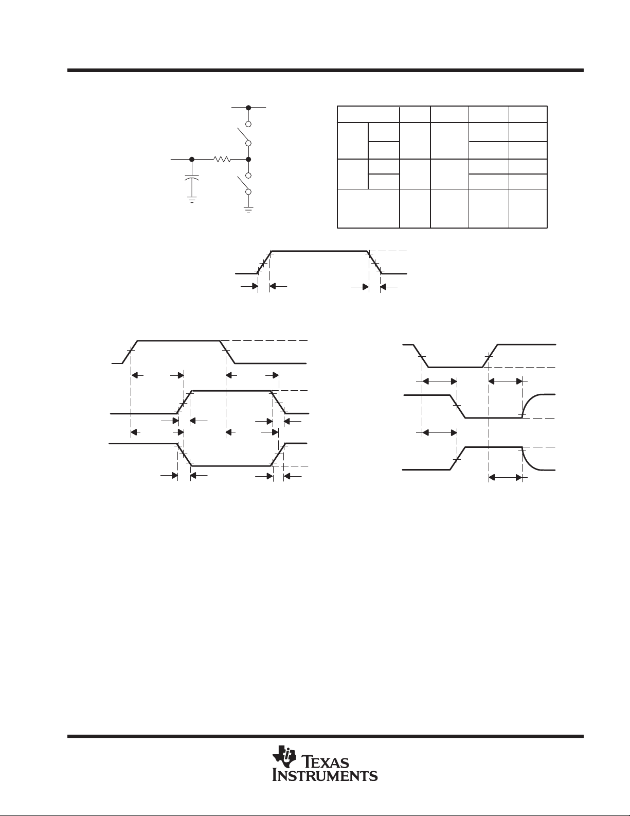
PARAMETER MEASUREMENT INFORMATION
V
From Output
Under Test
(see Note A)
Test
Point
C
L
LOAD CIRCUIT
CC
S1
R
L
S2
PARAMETER C
t
t
PZH
t
PZL
t
PHZ
t
PLZ
t
en
t
dis
tpd or t
R
1 kΩ
1 kΩ
L
50 pF
150 pF
50 pF
50 pF
150 pF
L
or
Closed Open
Closed Open
or
S1
Open Closed
Open Closed
Open Open––
S2
Input
Input
In-Phase
Output
Out-of-
Phase
Output
PROPAGATION DELAY AND OUTPUT RISE AND FALL TIMES
NOTES: A. CL includes probe and test-fixture capacitance.
B. Waveform 1 is for an output with internal conditions such that the output is low except when disabled by the output control.
C. Phase relationships between waveforms were chosen arbitrarily. All input pulses are supplied by generators having the following
D. The outputs are measured one at a time with one input transition per measurement.
E. t
F. t
G. t
1.3 V
t
PLH
90% 90%
t
PHL
1.3 V 1.3 V
10% 10%
VOLTAGE WAVEFORMS
Waveform 2 is for an output with internal conditions such that the output is high except when disabled by the output control.
characteristics: PRR ≤ 1 MHz, ZO = 50 Ω, tr = 6 ns, tf = 6 ns.
PLZ
PZL
PLH
and t
and t
and t
are the same as t
PHZ
are the same as ten.
PZH
are the same as tpd.
PHL
1.3 V
t
PHL
t
r
t
PLH
t
f
dis
2.7 V 2.7 V
VOLTAGE WAVEFORM
INPUT RISE AND FALL TIMES
.
3 V
1.3 V1.3 V
0.3 V0.3 V
0 V
t
r
3 V
0 V
V
1.3 V1.3 V
OH
10%10%
V
OL
t
f
V
OH
90%90%
V
OL
t
r
Output
Control
(Low-Level
Enabling)
Output
Waveform 1
(See Note B)
Output
Waveform 2
(See Note B)
ENABLE AND DISABLE TIMES FOR 3-STATE OUTPUTS
t
f
1.3 V
t
PZL
t
PZH
VOLTAGE WAVEFORMS
1.3 V
1.3 V
1.3 V
t
PLZ
10%
90%
t
PHZ
3 V
0 V
≈ V
V
OL
V
OH
≈ 0 V
CC
Figure 1. Load Circuit and Voltage Waveforms
POST OFFICE BOX 655303 • DALLAS, TEXAS 75265
5
Page 6

IMPORTANT NOTICE
T exas Instruments and its subsidiaries (TI) reserve the right to make changes to their products or to discontinue
any product or service without notice, and advise customers to obtain the latest version of relevant information
to verify, before placing orders, that information being relied on is current and complete. All products are sold
subject to the terms and conditions of sale supplied at the time of order acknowledgement, including those
pertaining to warranty, patent infringement, and limitation of liability.
TI warrants performance of its semiconductor products to the specifications applicable at the time of sale in
accordance with TI’s standard warranty. Testing and other quality control techniques are utilized to the extent
TI deems necessary to support this warranty . Specific testing of all parameters of each device is not necessarily
performed, except those mandated by government requirements.
CERTAIN APPLICA TIONS USING SEMICONDUCT OR PRODUCTS MAY INVOLVE POTENTIAL RISKS OF
DEATH, PERSONAL INJURY, OR SEVERE PROPERTY OR ENVIRONMENTAL DAMAGE (“CRITICAL
APPLICATIONS”). TI SEMICONDUCTOR PRODUCTS ARE NOT DESIGNED, AUTHORIZED, OR
WARRANTED TO BE SUITABLE FOR USE IN LIFE-SUPPORT DEVICES OR SYSTEMS OR OTHER
CRITICAL APPLICA TIONS. INCLUSION OF TI PRODUCTS IN SUCH APPLICATIONS IS UNDERST OOD TO
BE FULLY AT THE CUSTOMER’S RISK.
In order to minimize risks associated with the customer’s applications, adequate design and operating
safeguards must be provided by the customer to minimize inherent or procedural hazards.
TI assumes no liability for applications assistance or customer product design. TI does not warrant or represent
that any license, either express or implied, is granted under any patent right, copyright, mask work right, or other
intellectual property right of TI covering or relating to any combination, machine, or process in which such
semiconductor products or services might be or are used. TI’s publication of information regarding any third
party’s products or services does not constitute TI’s approval, warranty or endorsement thereof.
Copyright 1998, Texas Instruments Incorporated
 Loading...