

Page 1
B1
DIR
5
7
A1
2
V
CCA
V
CCB
B2
6
A2
3
1
8
VCCA
VCCB
GND
4
V
CCA
V
CCB
Product
Folder
Sample &
Buy
Technical
Documents
Tools &
Software
Support &
Community
SN74AVCH2T45
SCES582H –JULY 2004–REVISED APRIL 2015
SN74AVCH2T45 2-Bit, 2-Supply, Bus Transceiver with Configurable Level-Shifting and
Translation and 3-State Outputs
1 Features 3 Description
1
• Available in the Texas Instruments NanoFree™
Package
• VCCIsolation
• 2-Rail Design
• I/Os are 4.6 V Tolerant
• Partial Power-Down-Mode Operation
• Bus Hold on Data Inputs
• Maximum Data Rates
– 500 Mbps (1.8 V to 3.3 V)
– 320 Mbps (< 1.8 V to 3.3 V)
– 320 Mbps (Level-Shifting to 2.5 V or 1.8 V)
– 280 Mbps (Level-Shifting to 1.5 V)
– 240 Mbps (Level-Shifting to 1.2 V)
• Latch-Up Performance Exceeds 100 mA Per
JESD 78, Class II
• ESD Protection Exceeds JESD 22
2 Applications
• Smartphone
• Servers
• Desktop PCs and Notebooks
• Other Portable Devices
This 2-bit non-inverting bus transceiver uses two
separate configurable power-supply rails. The A ports
are designed to track V
and accepts any supply
CCA
voltage from 1.2 V to 3.6 V. The B ports are designed
to track V
and accepts any supply voltage from
CCB
1.2 V to 3.6 V. This allows for universal low-voltage
bidirectional translation and level-shifting between
any of the 1.2 V, 1.5 V, 1.8 V, 2.5 V, and 3.3 V
voltage nodes.
The SN74AVCH2T45 is designed for asynchronous
communication between two data buses. The logic
levels of the direction-control (DIR pin) input activate
either the B-port outputs or the A-port outputs. The
device transmits data from the A bus to the B bus
when the B-port outputs are activated and from the B
bus to the A bus when the A-port outputs are
activated. The SN74AVCH2T45 features active bushold circuitry, which holds unused or un-driven inputs
at a valid logic state. TI does not recommend using
pull-up or pull-down resistors with the bus-hold
circuitry.
Device Information
PART NUMBER PACKAGE BODY SIZE (NOM)
SSOP (8) 2.95 mm × 2.80 mm
SN74AVCH2T45 VSSOP (8) 2.30 mm × 2.00 mm
DSBGA (8) 1.89 mm × 0.89 mm
(1) For all available packages, see the orderable addendum at
the end of the data sheet.
(1)
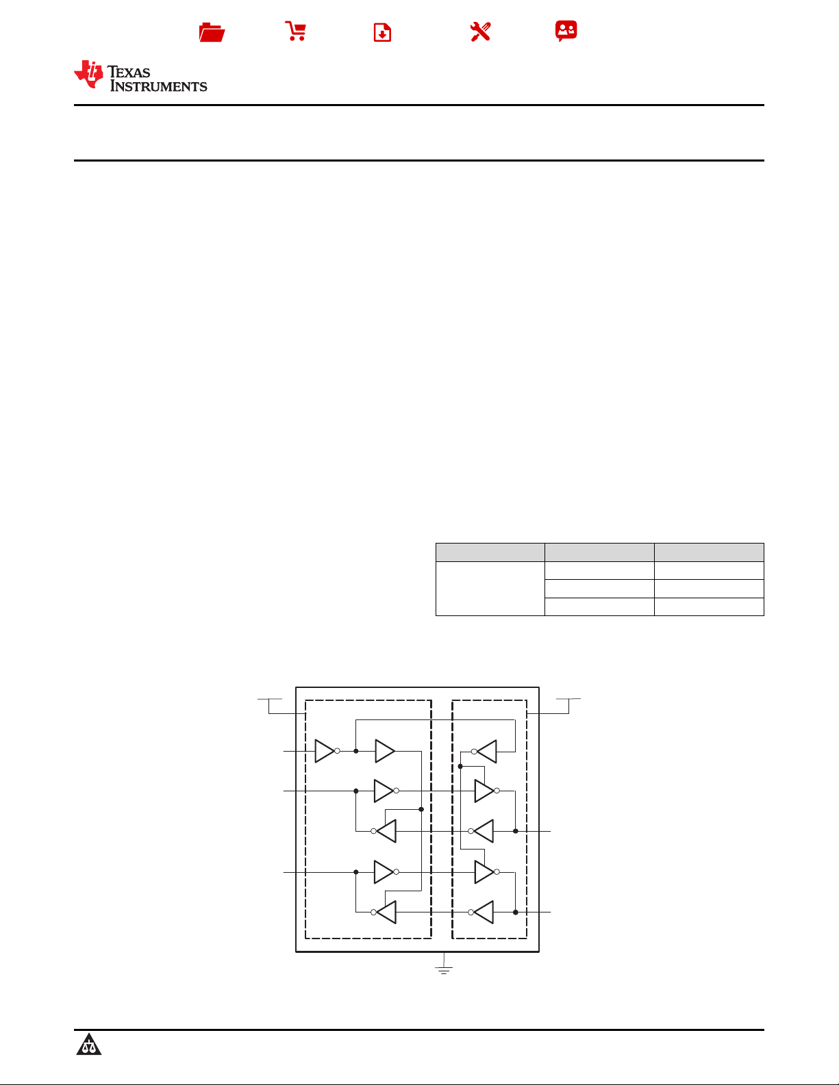
Logic Diagram (Positive Logic)
1
An IMPORTANT NOTICE at the end of this data sheet addresses availability, warranty, changes, use in safety-critical applications,
intellectual property matters and other important disclaimers. PRODUCTION DATA.
Page 2

SN74AVCH2T45
SCES582H –JULY 2004–REVISED APRIL 2015
www.ti.com
Table of Contents
1 Features.................................................................. 1 8 Parameter Measurement Information ................ 13
2 Applications ........................................................... 1 9 Detailed Description ............................................ 14
3 Description ............................................................. 1
4 Revision History..................................................... 3
5 Description (Continued)........................................ 4
6 Pin Configurations and Functions....................... 4
7 Specifications......................................................... 5
7.1 Absolute Maximum Ratings ...................................... 5
7.2 ESD Ratings.............................................................. 5
7.3 Recommended Operating Conditions ...................... 6
7.4 Thermal Information.................................................. 7
7.5 Electrical Characteristics .......................................... 7
7.6 Switching Characteristics: V
7.7 Switching Characteristics: V
7.8 Switching Characteristics: V
7.9 Switching Characteristics: V
7.10 Switching Characteristics: V
7.11 Operating Characteristics...................................... 11
7.12 Typical Characteristics.......................................... 12 14 Mechanical, Packaging, and Orderable
= 1.2 V ................... 8
CCA
= 1.5 V .................. 9
CCA
= 1.8 V ................. 10
CCA
= 2.5 V ................. 10
CCA
= 3.3 V ............... 11
CCA
9.1 Overview................................................................. 14
9.2 Functional Block Diagram....................................... 14
9.3 Feature Description................................................. 15
9.4 Device Functional Modes........................................ 15
10 Application and Implementation........................ 16
10.1 Application Information.......................................... 16
10.2 Typical Applications .............................................. 16
11 Power Supply Recommendations ..................... 20
12 Layout................................................................... 20
12.1 Layout Guidelines ................................................. 20
12.2 Layout Example .................................................... 20
13 Device and Documentation Support ................. 21
13.1 Documentation Support ....................................... 21
13.2 Trademarks........................................................... 21
13.3 Electrostatic Discharge Caution............................ 21
13.4 Glossary................................................................ 21
Information........................................................... 21
2 Submit Documentation Feedback Copyright © 2004–2015, Texas Instruments Incorporated
Product Folder Links: SN74AVCH2T45
Page 3

SN74AVCH2T45
www.ti.com
SCES582H –JULY 2004–REVISED APRIL 2015
4 Revision History
Changes from Revision G (April 2015) to Revision H Page
• Added additional applications................................................................................................................................................. 1
• Updated Overview section. .................................................................................................................................................. 14
• Updated Layout Guidelines section. .................................................................................................................................... 20
Changes from Revision F (November 2007) to Revision G Page
• Added ESD Ratings table, Feature Description section, Device Functional Modes, Application and Implementation
section, Power Supply Recommendations section, Layout section, Device and Documentation Support section, and
Mechanical, Packaging, and Orderable Information section ................................................................................................. 1
Copyright © 2004–2015, Texas Instruments Incorporated Submit Documentation Feedback 3
Product Folder Links: SN74AVCH2T45
Page 4
4
3
2
1
5
6
7
8
GND
A2
A1
V
CCA
DIR
B2
B1
V
CCB
D1 D2
C2C1
B1 B2
A1 A2
1
2
3
4
8
7
6
5
V
CCA
A1
A2
GND
V
CCB
B1
B2
DIR
SN74AVCH2T45
SCES582H –JULY 2004–REVISED APRIL 2015
www.ti.com
5 Description (Continued)
This device is fully specified for partial-power-down applications using I
preventing damaging current backflow through the device when it is powered down. The VCCisolation feature
ensures that if either VCCinput is at GND, then both outputs are in the high-impedance state. The bus-hold
circuitry on the powered-up side always stays active.
Active bus-hold circuitry holds unused or un-driven inputs at a valid logic state. NanoFree package technology is
a major breakthrough in IC packaging concepts, using the die as the package.
. The I
off
circuitry disables the outputs,
off
6 Pin Configurations and Functions
DCT and DCU Packages
8-Pin SSOP and VSSOP
Top View
YZP Package
8-Pin DSBGA
Bottom View
Pin Functions
PIN
NAME DSBGA
SSOP,
VSSOP
VCCA 1 A1 Supply Voltage A
VCCB 8 A2 Supply Voltage B
GND 4 D1 Ground
A1 2 B1 Output or input depending on state of DIR. Output level depends on V
A2 3 C1 Output or input depending on state of DIR. Output level depends on V
B1 7 B2 Output or input depending on state of DIR. Output level depends on V
B2 6 C2 Output or input depending on state of DIR. Output level depends on V
DIR 5 D2 Direction Pin, Connect to GND or to VCCA.
DESCRIPTION
CCA
CCA
CCB
CCB
.
.
.
.
4 Submit Documentation Feedback Copyright © 2004–2015, Texas Instruments Incorporated
Product Folder Links: SN74AVCH2T45
Page 5
SN74AVCH2T45
www.ti.com
SCES582H –JULY 2004–REVISED APRIL 2015
7 Specifications
7.1 Absolute Maximum Ratings
(2)(3)
(1)
MIN MAX UNIT
I/O ports (A port) –0.5 4.6
I/O ports (B port) –0.5 4.6 V
Control inputs –0.5 4.6
A port –0.5 4.6
B port –0.5 4.6
A port –0.5 V
B port –0.5 V
CCA
CCB
+ 0.5
+ 0.5
V
V
over operating free-air temperature range (unless otherwise noted)
V
CCA
V
V
V
V
I
IK
I
OK
I
O
T
J
T
stg
(1) Stresses beyond those listed under Absolute Maximum Ratings may cause permanent damage to the device. These are stress ratings
(2) The input voltage and output negative-voltage ratings may be exceeded if the input and output current ratings are observed.
(3) The output positive-voltage rating may be exceeded up to 4.6 V maximum if the output current rating is observed.
Supply voltage –0.5 4.6 V
CCB
Input voltage
I
Voltage range applied to any output
O
in the high-impedance or power-off state
Voltage range applied to any output in the high or low state
O
(2)
(2)
Input clamp current VI< 0 –50 mA
Output clamp current VO< 0 –50 mA
Continuous output current ±50 mA
Continuous current through V
CCA
, V
, or GND ±100 mA
CCB
Junction temperature –40 150 °C
Storage temperature –65 150 °C
only, which do not imply functional operation of the device at these or any other conditions beyond those indicated under Recommended
Operating Conditions. Exposure to absolute-maximum-rated conditions for extended periods may affect device reliability.
7.2 ESD Ratings
Human body model (HBM), per ANSI/ESDA/JEDEC JS-001
V
(ESD)
Electrostatic discharge ±1000 V
Charged-device model (CDM), per JEDEC specification JESD22-
(2)
C101
Machine Model (MM), Per JEDEC specification JESD22-A115-A ±200
(1) JEDEC document JEP155 states that 500-V HBM allows safe manufacturing with a standard ESD control process.
(2) JEDEC document JEP157 states that 250-V CDM allows safe manufacturing with a standard ESD control process.
(1)
VALUE UNIT
±8000
Copyright © 2004–2015, Texas Instruments Incorporated Submit Documentation Feedback 5
Product Folder Links: SN74AVCH2T45
Page 6
SN74AVCH2T45
SCES582H –JULY 2004–REVISED APRIL 2015
www.ti.com
7.3 Recommended Operating Conditions
over operating free-air temperature range (unless otherwise noted)
(4)
V
CCI
V
Supply voltage 1.2 3.6 V
CCA
V
Supply voltage 1.2 3.6 V
CCB
High-level
V
input Data inputs
IH
voltage
Low-level
V
input Data inputs
IL
voltage
(2)
(2)
High-level DIR
V
input (referenced to 1.95 V to 2.7 V 1.6 V
IH
voltage V
CCA
(3)
)
Low-level DIR
V
input (referenced to 1.95 V to 2.7 V 0.7 V
IL
voltage V
V
Input voltage 0 3.6 V
I
Output
V
O
voltage
I
High-level output current –8 mA
OH
I
Low-level output current 8 mA
OL
(3)
)
CCA
Active state 0 V
3-state 0 3.6
Δt/Δv Input transition rise or fall rate 5 ns/V
T
Operating free-air temperature –40 85 °C
A
(1) All unused data inputs of the device must be held at V
Implications of Slow or Floating CMOS Inputs, SCBA004.
(2) For V
(3) For V
(4) V
(5) V
values not specified in the data sheet, VIHmin = V
CCI
values not specified in the data sheet, VIHmin = V
CCI
is the voltage associated with the input port supply VCCA or VCCB.
CCI
is the voltage associated with the output port supply VCCA or VCCB.
CCO
1.2 V to 1.95 V V
1.95 V to 2.7 V 1.6 V
2.7 V to 3.6 V 2
1.2 V to 1.95 V V
1.95 V to 2.7 V 0.7 V
2.7 V to 3.6 V 0.8
1.2 V to 1.95 V V
2.7 V to 3.6 V 2
1.2 V to 1.95 V V
2.7 V to 3.6 V 0.8
1.4 V to 1.6 V –6
1.65 V to 1.95
2.3 V to 2.7 V –9
1.4 V to 1.6 V 6
1.65 V to 1.95
2.3 V to 2.7 V 9
or GND to ensure proper device operation. Refer to the TI application report,
CCI
CCI
CCA
(1)(2)(3)
(5)
V
CCO
MIN NOM MAX UNIT
(4)
× 0.65
CCI
CCI
× 0.65
CCA
CCA
(4)
× 0.35
× 0.35
CCO
1.2 V –3
V
3 V to 3.6 V –12
1.2 V 3
V
3 V to 3.6 V 12
× 0.7 V, VILmax = V
× 0.7 V, VILmax = V
CCI
CCA
× 0.3 V.
× 0.3 V.
(5)
V
6 Submit Documentation Feedback Copyright © 2004–2015, Texas Instruments Incorporated
Product Folder Links: SN74AVCH2T45
Page 7
SN74AVCH2T45
www.ti.com
SCES582H –JULY 2004–REVISED APRIL 2015
7.4 Thermal Information
SN74AVCH2T45
THERMAL METRIC
(1)
DCT (SSOP) DCU (VSSOP) YZP (DSBGA) UNIT
8 PINS 8 PINS 8 PINS
R
θJA
R
θJC(top)
R
θJB
ψ
JT
ψ
JB
Junction-to-ambient thermal resistance 194.4 199.3 105.8
Junction-to-case (top) thermal resistance 124.7 76.2 1.6
Junction-to-board thermal resistance 106.8 80.6 10.8 °C/W
Junction-to-top characterization parameter 49.8 7.1 3.1
Junction-to-board characterization parameter 105.8 80.1 10.8
(1) For more information about traditional and new thermal metrics, see the IC Package Thermal Metrics application report, SPRA953.
7.5 Electrical Characteristics
over recommended operating free-air temperature range (unless otherwise noted)
PARAMETER TEST CONDITIONS V
IOH= –100 μA 1.2 V to 3.6 V 1.2 V to 3.6 V V
IOH= –3 mA 1.2 V 1.2 V 0.95
(3)
V
OH
IOH= –6 mA 1.4 V 1.4 V 1.05
IOH= –8 mA 1.65 V 1.65 V 1.2
VI= V
IH
IOH= –9 mA 2.3 V 2.3 V 1.75
IOH= –12 mA 3 V 3 V 2.3
IOL= 100 μA 1.2 V to 3.6 V 1.2 V to 3.6 V 0.2
IOL= 3 mA 1.2 V 1.2 V 0.15
(3)
V
OL
IOL= 6 mA 1.4 V 1.4 V 0.35
IOL= 8 mA 1.65 V 1.65 V 0.45
VI= V
IL
IOL= 9 mA 2.3 V 2.3 V 0.55
IOL= 12 mA 3 V 3 V 0.7
(3)
I
I
DIR input VI= V
or GND 1.2 V to 3.6 V 1.2 V to 3.6 V ±0.025 ±0.25 ±1 μA
CCA
VI= 0.42 V 1.2 V 1.2 V 25
VI= 0.49 V 1.4 V 1.4 V 15
(4)
I
BHL
VI= 0.58 V 1.65 V 1.65 V 25 μA
VI= 0.7 V 2.3 V 2.3 V 45
VI= 0.8 V 3.3 V 3.3 V 100
VI= 0.78 V 1.2 V 1.2 V –25
VI= 0.91 V 1.4 V 1.4 V –15
(5)
I
BHH
VI= 1.07 V 1.65 V 1.65 V –25 μA
VI= 1.6 V 2.3 V 2.3 V –45
VI= 2 V 3.3 V 3.3 V –100
(6)
I
BHLO
VI= 0 to V
CC
CCA
V
CCB
1.2 V 1.2 V 50
1.6 V 1.6 V 125
1.95 V 1.95 V 200 μA
2.7 V 2.7 V 300
3.6 V 3.6 V 500
TA= 25°C –40°C to 85°C
MIN TYP MAX MIN TYP MAX
(1)(2)
CCO
– 0.2
UNIT
V
V
(1) V
(2) V
(3) VOH: Output High Voltage; VOL: Output Low Voltage; II: Control Input Current.
(4) The bus-hold circuit can sink at least the minimum low sustaining current at VILmaximum. I
(5) The bus-hold circuit can source at least the minimum high sustaining current at VIHmininum. I
(6) An external driver must source at least I
is the voltage associated with the output port supply VCCA or VCCB.
CCO
is the voltage associated with the input port supply VCCA or VCCB.
CCI
GND and then raising it to VILmaximum.
to VCCand then lowering it to VIHminimum.
to switch this node from low to high.
BHLO
should be measured after lowering VINto
BHL
should be measured after raising V
BHH
IN
Copyright © 2004–2015, Texas Instruments Incorporated Submit Documentation Feedback 7
Product Folder Links: SN74AVCH2T45
Page 8
SN74AVCH2T45
SCES582H –JULY 2004–REVISED APRIL 2015
Electrical Characteristics (continued)
over recommended operating free-air temperature range (unless otherwise noted)
PARAMETER TEST CONDITIONS V
CCA
1.2 V 1.2 V –50
1.6 V 1.6 V –125
(7)
I
BHHO
VI= 0 to V
CC
1.95 V 1.95 V –200 μA
2.7 V 2.7 V –300
3.6 V 3.6 V –500
A port 0 V 0 V to 3.6 V ±0.1 ±1 ±5
(8)
I
off
B port 0 V to 3.6 V 0 V ±0.1 ±1 ±5
B port 0 V 3.6 V ±0.5 ±2.5 ±5
(8)
I
OZ
A port 3.6 V 0 V ±0.5 ±2.5 ±5 μA
VIor VO= 0 to 3.6 V μA
VO= V
VI= V
CCO
CCI
or GND,
or GND
1.2 V to 3.6 V 1.2 V to 3.6 V 10
(8)
I
CCA
VI= V
or GND, IO= 0 0 V 3.6 V –2 μA
CCI
3.6 V 0 V 10
1.2 V to 3.6 V 1.2 V to 3.6 V 10
(8)
I
CCB
VI= V
or GND, IO= 0 0 V 3.6 V 10 μA
CCI
3.6 V 0 V –2
I
+ I
CCA
CCB
Control
C
i
inputs
C
A or B port VI= 3.3 V or GND 3.3 V 3.3 V 6 pF
io
(7) An external driver must sink at least I
(8) I
: Partial Power Down Output current; IOZ: Hi-Z Output Current; I
off
VI= V
or GND, IO= 0 1.2 V to 3.6 V 1.2 V to 3.6 V 20 μA
CCI
VI= 3.3 V or GND 3.3 V 3.3 V 2.5 pF
to switch this node from high to low.
BHHO
V
CCB
: Supply A Current; I
CCA
TA= 25°C –40°C to 85°C
MIN TYP MAX MIN TYP MAX
(1)(2)
: Supply B Current.
CCB
www.ti.com
UNIT
7.6 Switching Characteristics: V
over recommended operating free-air temperature range, V
PARAMETER UNIT
(1)
t
PLH
(1)
t
PHL
(1)
t
PLH
(1)
t
PHL
(1)
t
PHZ
(1)
t
PLZ
(1)
t
PHZ
(1)
t
PLZ
(1)(2)
t
PZH
(1)(2)
t
PZL
(1)(2)
t
PZH
(1)(2)
t
PZL
(1) t
: Low-to-high Propagation Delay; t
PLH
Propagation Delay; t
(2) The enable time is a calculated value derived using the formula shown in the Enable Times section.
FROM TO
(INPUT) (OUTPUT)
A B ns
B A ns
DIR A ns
DIR B ns
DIR A ns
DIR B ns
: Hi-Z-to-High Propagation Delay; t
PZH
PHL
= 1.2 V
CCA
= 1.2 V (see Figure 7)
CCA
V
= 1.2 V V
CCB
= 1.5 V V
CCB
= 1.8 V V
CCB
= 2.5 V V
CCB
TYP TYP TYP TYP TYP
3.1 2.6 2.4 2.2 2.2
3.1 2.6 2.4 2.2 2.2
3.4 3.1 3 2.9 2.9
3.4 3.1 3 2.9 2.9
5.2 5.2 5.1 5 4.8
5.2 5.2 5.1 5 4.8
5 4 3.8 2.8 3.2
5 4 3.8 2.8 3.2
8.4 7.1 6.8 5.7 6.1
8.4 7.1 6.8 5.7 6.1
8.3 7.8 7.5 7.2 7
8.3 7.8 7.5 7.2 7
: High-to-Low Propagation Delay; t
: Hi-Z-to-Low Propagation Delay
PZL
: High-to-Hi-Z Propagation Delay; t
PHZ
= 3.3 V
CCB
: Low-to-Hi-Z
PLZ
8 Submit Documentation Feedback Copyright © 2004–2015, Texas Instruments Incorporated
Product Folder Links: SN74AVCH2T45
Page 9
www.ti.com
SN74AVCH2T45
SCES582H –JULY 2004–REVISED APRIL 2015
7.7 Switching Characteristics: V
over recommended operating free-air temperature range, V
PARAMETER UNIT
(1)
t
PLH
(1)
t
PHL
(1)
t
PLH
(1)
t
PHL
(1)
t
PHZ
(1)
t
PLZ
(1)
t
PHZ
(1)
t
PLZ
(1)(2)
t
PZH
(1)(2)
t
PZL
(1)(2)
t
PZH
(1)(2)
t
PZL
(1) t
: Low-to-high Propagation Delay; t
PLH
Propagation Delay; t
(2) The enable time is a calculated value derived using the formula shown in the Enable Times section.
FROM TO
(INPUT) (OUTPUT)
A B ns
B A ns
DIR A ns
DIR B ns
DIR A ns
DIR B ns
: Hi-Z-to-High Propagation Delay; t
PZH
PHL
= 1.5 V
CCA
= 1.5 V ± 0.1 V (see Figure 7)
CCA
V
= 1.5 V V
V
= 1.2 V
CCB
CCB
± 0.1 V ± 0.15 V ± 0.2 V ± 0.3 V
= 1.8 V V
CCB
= 2.5 V V
CCB
TYP MIN MAX MIN MAX MIN MAX MIN MAX
2.8 0.7 5.4 0.5 4.6 0.4 3.7 0.3 3.5
2.8 0.7 5.4 0.5 4.6 0.4 3.7 0.3 3.5
2.7 0.8 5.4 0.7 5.2 0.6 4.9 0.5 4.7
2.7 0.8 5.4 0.7 5.2 0.6 4.9 0.5 4.7
3.9 1.3 8.5 1.3 7.8 1.1 7.7 1.4 7.6
3.9 1.3 8.5 1.3 7.8 1.1 7.7 1.4 7.6
4.7 1.1 7 1.4 6.9 1.2 6.9 1.7 7.1
4.7 1.1 7 1.4 6.9 1.2 6.9 1.7 7.1
7.4 12.4 12.1 11.8 11.8
7.4 12.4 12.1 11.8 11.8
6.7 13.9 12.4 11.4 11.1
6.7 13.9 12.4 11.4 11.1
: High-to-Low Propagation Delay; t
: Hi-Z-to-Low Propagation Delay
PZL
: High-to-Hi-Z Propagation Delay; t
PHZ
= 3.3 V
CCB
: Low-to-Hi-Z
PLZ
Copyright © 2004–2015, Texas Instruments Incorporated Submit Documentation Feedback 9
Product Folder Links: SN74AVCH2T45
Page 10
SN74AVCH2T45
SCES582H –JULY 2004–REVISED APRIL 2015
www.ti.com
7.8 Switching Characteristics: V
over recommended operating free-air temperature range, V
PARAMETER UNIT
(1)
t
PLH
(1)
t
PHL
(1)
t
PLH
(1)
t
PHL
(1)
t
PHZ
(1)
t
PLZ
(1)
t
PHZ
(1)
t
PLZ
(1)(2)
t
PZH
(1)(2)
t
PZL
(1)(2)
t
PZH
(1)(2)
t
PZL
(1) t
: Low-to-high Propagation Delay; t
PLH
Propagation Delay; t
(2) The enable time is a calculated value derived using the formula shown in the Enable Times section.
FROM TO
(INPUT) (OUTPUT)
A B ns
B A ns
DIR A ns
DIR B ns
DIR A ns
DIR B ns
: Hi-Z-to-High Propagation Delay; t
PZH
PHL
7.9 Switching Characteristics: V
over recommended operating free-air temperature range, V
PARAMETER UNIT
(1)
t
PLH
(1)
t
PHL
(1)
t
PLH
(1)
t
PHL
(1)
t
PHZ
(1)
t
PLZ
(1)
t
PHZ
(1)
t
PLZ
(1)(2)
t
PZH
(1)(2)
t
PZL
(1)(2)
t
PZH
(1)(2)
t
PZL
(1) t
: Low-to-high Propagation Delay; t
PLH
Propagation Delay; t
(2) The enable time is a calculated value derived using the formula shown in the Enable Times section.
FROM TO
(INPUT) (OUTPUT)
A B ns
B A ns
DIR A ns
DIR B ns
DIR A ns
DIR B ns
: Hi-Z-to-High Propagation Delay; t
PZH
PHL
= 1.8 V
CCA
= 1.8 V ± 0.15 V (see Figure 7)
CCA
V
= 1.5 V V
V
= 1.2 V
CCB
CCB
± 0.1 V ± 0.15 V ± 0.2 V ± 0.3 V
= 1.8 V V
CCB
= 2.5 V V
CCB
TYP MIN MAX MIN MAX MIN MAX MIN MAX
2.7 0.5 5.2 0.4 4.3 0.2 3.4 0.2 3.1
2.7 0.5 5.2 0.4 4.3 0.2 3.4 0.2 3.1
2.4 0.7 4.7 0.5 4.4 0.5 4 0.4 3.8
2.4 0.7 4.7 0.5 4.4 0.5 4 0.4 3.8
3.7 1.3 8.1 0.7 6.9 1.4 5.3 1.1 5.2
3.7 1.3 8.1 0.7 6.9 1.4 5.3 1.1 5.2
4.4 1.3 5.8 1.3 5.9 0.8 5.7 1.5 5.9
4.4 1.3 5.8 1.3 5.9 0.8 5.7 1.5 5.9
6.8 10.5 10.3 9.7 9.7
6.8 10.5 10.3 9.7 9.7
6.4 13.3 11.2 8.7 8.3
6.4 13.3 11.2 8.7 8.3
: High-to-Low Propagation Delay; t
: Hi-Z-to-Low Propagation Delay
PZL
= 2.5 V
CCA
= 2.5 V ± 0.2 V (see Figure 7)
CCA
V
= 1.5 V V
V
= 1.2 V
CCB
CCB
± 0.1 V ± 0.15 V ± 0.2 V ± 0.3 V
: High-to-Hi-Z Propagation Delay; t
PHZ
= 1.8 V V
CCB
= 2.5 V V
CCB
TYP MIN MAX MIN MAX MIN MAX MIN MAX
2.6 0.4 4.9 0.2 4 0.2 3 0.2 2.6
2.6 0.4 4.9 0.2 4 0.2 3 0.2 2.6
2.1 0.6 3.8 0.5 3.4 0.4 3 0.3 2.8
2.1 0.6 3.8 0.5 3.4 0.4 3 0.3 2.8
2.4 0.7 7.9 0.8 6.4 0.8 5 0.5 4.3
2.4 0.7 7.9 0.8 6.4 0.8 5 0.5 4.3
3.8 1 4.3 0.6 4.3 0.5 4.2 1.1 4.1
3.8 1 4.3 0.6 4.3 0.5 4.2 1.1 4.1
5.9 8.5 7.7 7.2 6.9
5.9 8.5 7.7 7.2 6.9
5 12.8 10.4 8 6.9
5 12.8 10.4 8 6.9
: High-to-Low Propagation Delay; t
: Hi-Z-to-Low Propagation Delay
PZL
: High-to-Hi-Z Propagation Delay; t
PHZ
= 3.3 V
CCB
: Low-to-Hi-Z
PLZ
= 3.3 V
CCB
: Low-to-Hi-Z
PLZ
10 Submit Documentation Feedback Copyright © 2004–2015, Texas Instruments Incorporated
Product Folder Links: SN74AVCH2T45
Page 11
www.ti.com
SN74AVCH2T45
SCES582H –JULY 2004–REVISED APRIL 2015
7.10 Switching Characteristics: V
over recommended operating free-air temperature range, V
PARAMETER UNIT
(1)
t
PLH
(1)
t
PHL
(1)
t
PLH
(1)
t
PHL
(1)
t
PHZ
(1)
t
PLZ
(1)
t
PHZ
(1)
t
PLZ
(1)(2)
t
PZH
(1)(2)
t
PZL
(1)(2)
t
PZH
(1)(2)
t
PZL
(1) t
: Low-to-high Propagation Delay; t
PLH
Propagation Delay; t
(2) The enable time is a calculated value derived using the formula shown in the Enable Times section.
FROM TO
(INPUT) (OUTPUT)
A B ns
B A ns
DIR A ns
DIR B ns
DIR A ns
DIR B ns
: High-to-Low Propagation Delay; t
: Hi-Z-to-High Propagation Delay; t
PZH
PHL
= 3.3 V
CCA
= 3.3 V ± 0.3 V (see Figure 7)
CCA
V
= 1.5 V V
V
= 1.2 V
CCB
CCB
± 0.1 V ± 0.15 V ± 0.2 V ± 0.3 V
= 1.8 V V
CCB
= 2.5 V V
CCB
CCB
TYP MIN MAX MIN MAX MIN MAX MIN MAX
2.5 0.3 4.7 0.2 3.8 0.2 2.8 0.2 2.4
2.5 0.3 4.7 0.2 3.8 0.2 2.8 0.2 2.4
2.1 0.6 3.6 0.4 3.1 0.3 2.6 0.3 2.4
2.1 0.6 3.6 0.4 3.1 0.3 2.6 0.3 2.4
2.9 1.1 8 1 6.5 1.3 4.7 1.2 4
2.9 1.1 8 1 6.5 1.3 4.7 1.2 4
3.4 0.5 6.6 0.3 5.6 0.3 4.6 1.1 4.2
3.4 0.5 6.6 0.3 5.6 0.3 4.6 1.1 4.2
5.5 10.2 8.7 7.2 6.6
5.5 10.2 8.7 7.2 6.6
5.4 12.7 10.3 7.5 6.4
5.4 12.7 10.3 7.5 6.4
: High-to-Hi-Z Propagation Delay; t
: Hi-Z-to-Low Propagation Delay
PZL
PHZ
PLZ
= 3.3 V
: Low-to-Hi-Z
7.11 Operating Characteristics
TA= 25°C
V
= V
PARAMETER UNIT
A-port input,
pdA
B-port input,
B-port output
(1)
C
A-port output
A-port input,
pdB
B-port input,
B-port output
(1)
C
A-port output
TEST
CONDITIONS
CL= 0,
f = 10 MHz, pF
(2)
(2)
t
= t
f
= 1 ns
r
CL= 0,
f = 10 MHz, pF
(2)
(2)
t
= t
f
= 1 ns
r
CCA
V
= 1.2 V V
CCB
TYP TYP TYP TYP TYP
3 3 3 3 4
13 13 14 15 15
13 13 14 15 15
3 3 3 3 4
(1) Power dissipation capacitance per transceiver
(2) tr: Rise time; tf: Fall time
CCA
= 1.5 V V
CCB
= V
CCB
= V
CCA
= 1.8 V V
CCA
= 2.5 V V
CCB
= V
CCB
CCA
= 3.3 V
=
Copyright © 2004–2015, Texas Instruments Incorporated Submit Documentation Feedback 11
Product Folder Links: SN74AVCH2T45
Page 12

0
1
2
3
4
5
6
0 10 20 30 40 50
t
PLH
- ns
C
L
- pF
60
V
CCB
= 1.8 V
V
CCB
= 2.5 V
V
CCB
= 3.3 V
V
CCB
= 1.5 V
V
CCB
= 1.2 V
t
PHL
- ns
CL - pF
0
1
2
3
4
5
6
0 10 20 30 40 50 60
V
CCB
= 1.8 V
V
CCB
= 2.5 V
V
CCB
= 3.3 V
V
CCB
= 1.5 V
V
CCB
= 1.2 V
0
1
2
3
4
5
6
0 10 20 30 40 50
t
PLH
(ns)
CL(pF)
60
V
CCB
= 1.8 V
V
CCB
= 2.5 V
V
CCB
= 3.3 V
V
CCB
= 1.5 V
V
CCB
= 1.2 V
t
PHL
(ns)
CL(pF)
0
1
2
3
4
5
6
0 10 20 30 40 50 60
V
CCB
= 1.8 V
V
CCB
= 2.5 V
V
CCB
= 3.3 V
V
CCB
= 1.5 V
V
CCB
= 1.2 V
0
1
2
3
4
5
6
0 10 20 30 40 50
t
PLH
(ns)
CL(pF)
60
V
CCB
= 1.8 V
V
CCB
= 2.5 V
V
CCB
= 3.3 V
V
CCB
= 1.5 V
V
CCB
= 1.2 V
0
1
2
3
4
5
6
0 10 20 30 40 50 60
t
PHL
(ns)
CL(pF)
V
CCB
= 1.8 V
V
CCB
= 2.5 V
V
CCB
= 3.3 V
V
CCB
= 1.5 V
V
CCB
= 1.2 V
SN74AVCH2T45
SCES582H –JULY 2004–REVISED APRIL 2015
7.12 Typical Characteristics
www.ti.com
7.12.1 Typical Propagation Delay (A to B) vs Load Capacitance, TA= 25°C, V
Figure 1. Typical A-to-B Propagation Delay, Low to High
Figure 2. Typical A-to-B Propagation Delay, High to Low
7.12.2 Typical Propagation Delay (A to B) vs Load Capacitance, TA= 25°C, V
CCA
CCA
= 1.8 V
= 2.5 V
Figure 3. Typical A-to-B Propagation Delay, Low to High
7.12.3 Typical Propagation Delay (A to B) vs Load Capacitance, TA= 25°C, V
Figure 5. Typical A-to-B Propagation Delay, Low to High
12 Submit Documentation Feedback Copyright © 2004–2015, Texas Instruments Incorporated
Figure 4. Typical A-to-B Propagation Delay, High to Low
= 3.3 V
CCA
Figure 6. Typical A-to-B Propagation Delay, High to Low
Product Folder Links: SN74AVCH2T45
Page 13

V
OH
V
OL
From Output
Under Test
C
L
(see Note A)
LOAD CIRCUIT
S1
2 × V
CCO
Open
GND
R
L
R
L
t
PLH
t
PHL
Output
Control
(low-level
enabling)
Output
Waveform 1
S1 at 2 × V
CCO
(see Note B)
Output
Waveform 2
S1 at GND
(see Note B)
t
PZL
t
PZH
t
PLZ
t
PHZ
V
CCA
/2V
CCA
/2
V
CCI
/2 V
CCI
/2
V
CCI
0 V
V
CCO
/2 V
CCO
/2
V
OH
V
OL
0 V
V
CCO
/2
VOL + V
TP
V
CCO
/2
VOH - V
TP
0 V
V
CCI
0 V
V
CCI
/2 V
CCI
/2
t
w
Input
V
CCA
V
CCO
VOLTAGE WAVEFORMS
PROPAGATION DELAY TIMES
VOLTAGE WAVEFORMS
PULSE DURATION
VOLTAGE WAVEFORMS
ENABLE AND DISABLE TIMES
Output
Input
t
pd
t
PLZ/tPZL
t
PHZ/tPZH
Open
2 × V
CCO
GND
TEST S1
NOTES: A. CL includes probe and jig capacitance.
B. Waveform 1 is for an output with internal conditions such that the output is low, except when disabled by the output control.
Waveform2 is for an output with internal conditions such that the output is high, except when disabled by the output control.
C. All input pulses are supplied by generators having the following characteristics: PRRv10 MHz, ZO = 50 Ω, dv/dt ≥ 1 V/ns.
D. The outputs are measured one at a time, with one transition per measurement.
E. t
PLZ
and t
PHZ
are the same as t
dis
.
F. t
PZL
and t
PZH
are the same as ten.
G. t
PLH
and t
PHL
are the same as tpd.
H. V
CCI
is the VCC associated with the input port.
I. V
CCO
is the VCC associated with the output port.
1.2 V
1.5 V ± 0.1 V
1.8 V ± 0.15 V
2.5 V ± 0.2 V
3.3 V ± 0.3 V
2 kΩ
2 kΩ
2 kΩ
2 kΩ
2 kΩ
V
CCO
R
L
0.1 V
0.1 V
0.15 V
0.15 V
0.3 V
V
TP
C
L
15 pF
15 pF
15 pF
15 pF
15 pF
www.ti.com
8 Parameter Measurement Information
SN74AVCH2T45
SCES582H –JULY 2004–REVISED APRIL 2015
Figure 7. Load Circuit and Voltage Waveforms
Copyright © 2004–2015, Texas Instruments Incorporated Submit Documentation Feedback 13
Product Folder Links: SN74AVCH2T45
Page 14

B1
DIR
5
7
A1
2
V
CCA
V
CCB
B2
6
A2
3
1
8
VCCA
VCCB
GND
4
V
CCA
V
CCB
SN74AVCH2T45
SCES582H –JULY 2004–REVISED APRIL 2015
www.ti.com
9 Detailed Description
9.1 Overview
This dual-bit non-inverting bus transceiver uses two separate configurable power-supply rails. The A port is
designed to track V
and accepts any supply voltage from 1.2 V to 3.6 V. This allows for universal low-voltage bidirectional translation
and level-shifting between any of the 1.2 V, 1.5 V, 1.8 V, 2.5 V, and 3.3 V voltage nodes.
The SN74AVCH2T45 is designed for asynchronous communication between two data buses. The logic levels of
the direction-control (DIR pin) input activate either the B-port outputs or the A-port outputs. The device transmits
data from the A bus to the B bus when the B-port outputs are activated and from the B bus to the A bus when
the A-port outputs are activated.
The SN74AVCH2T45 features active bus-hold circuitry.
The DIR input is powered by supply voltage from VCCA.
This device is fully specified for partial-power-down applications using off output current (I
disables the outputs, preventing damaging current backflow through the device when it is powered down.
The VCCisolation feature ensures that if either VCC input is at GND, both ports are put in a high-impedance
state. This will prevent a false high or low logic being presented at the output.
NanoFree package technology is a major breakthrough in IC packaging concepts, using the die as the package.
and accepts any supply voltage from 1.2 V to 3.6 V. The B port is designed to track V
CCA
). The I
off
circuitry
off
CCB
9.2 Functional Block Diagram
14 Submit Documentation Feedback Copyright © 2004–2015, Texas Instruments Incorporated
Product Folder Links: SN74AVCH2T45
Page 15

SN74AVCH2T45
www.ti.com
SCES582H –JULY 2004–REVISED APRIL 2015
9.3 Feature Description
9.3.1 VCC Isolation
The VCCisolation feature ensures that if either V
state (IOZshown in the Functional Block Diagram). This prevents false logic levels from being presented to either
bus.
9.3.2 2-Rail Design
Fully configurable 2-rail design allows each port to operate over the full 1.2 V to 3.6 V power-supply range.
9.3.3 IO Ports are 4.6 V Tolerant
The IO ports are up to 4.6 V tolerant
9.3.4 Partial Power Down Mode
This device is fully specified for partial-power-down applications using off output current (I
disables the outputs, preventing damaging current backflow through the device when it is powered down.
9.3.5 Bus Hold on Data Inputs
Active bus-hold circuitry holds unused or un-driven inputs at a valid logic state. TI does not recommend using
pull-up or pull-down resistors with the bus-hold circuitry.
CCA
or V
are at GND, both ports will be in a high-impedance
CCB
). The I
off
off
circuitry
9.4 Device Functional Modes
Table 1. Function Table (Each Transceiver)
INPUT
DIR
L B data to A bus
H A data to B bus
OPERATION
Copyright © 2004–2015, Texas Instruments Incorporated Submit Documentation Feedback 15
Product Folder Links: SN74AVCH2T45
Page 16

V
CCA
V
CCA
V
CCB
SYSTEM-1 SYSTEM-2
V
CCA
1
2
3
4
8
7
6
5
V
CCB
V
CCB
VCCB
B1
B2
DIR
VCCA
A2
A1
GND
SN74AVCH2T45
SCES582H –JULY 2004–REVISED APRIL 2015
www.ti.com
10 Application and Implementation
NOTE
Information in the following applications sections is not part of the TI component
specification, and TI does not warrant its accuracy or completeness. TI’s customers are
responsible for determining suitability of components for their purposes. Customers should
validate and test their design implementation to confirm system functionality.
10.1 Application Information
The SN74AVCH2T45 is used to shift IO voltage levels from one voltage domain to another. Each bus (bus A and
bus B) have independent power supplies, and a direction pin is used to control the direction of data flow.
10.2 Typical Applications
10.2.1 Unidirectional Logic Level-Shifting Application
Figure 8 is an example of the SN74AVCH2T45 circuit used in a unidirectional logic level-shifting application.
Figure 8. Unidirectional Logic Level-Shifting Application
10.2.1.1 Design Requirements
This device uses drivers which are enabled depending on the state of the DIR pin. The designer must know the
intended flow of data and take care not to violate any of the high or low logic levels. Active bus-hold circuitry
holds unused or un-driven inputs at a valid logic state. TI does not recommend using pull-up or pull-down
resistors with the bus-hold circuitry.
10.2.1.2 Detailed Design Procedure
Table 2 lists the pins and pin descriptions of the SN74AVCH2T45 connections with SYSTEM-1 and SYSTEM-2.
16 Submit Documentation Feedback Copyright © 2004–2015, Texas Instruments Incorporated
Product Folder Links: SN74AVCH2T45
Page 17

Magnitude (V)
-0.5
0
0.5
1
1.5
2
2.5
3
3.5
D002
Input
Output
www.ti.com
Typical Applications (continued)
Table 2. SN74AVCH2T45 Pin Connections With SYSTEM-1 and SYSTEM-2
PIN NAME DESCRIPTION
1 VCCA SYSTEM-1 supply voltage (1.2 V to 3.6 V)
2 A1 Output level depends on V
3 A2 Output level depends on V
4 GND Device GND
5 DIR The GND (low-level) determines B-port to A-port direction.
6 B2 Input threshold value depends on V
7 B1 Input threshold value depends on V
8 VCCB SYSTEM-2 supply voltage (1.2 V to 3.6 V)
10.2.1.3 Application Curve
CCA
CCA
.
.
CCB
CCB
SN74AVCH2T45
SCES582H –JULY 2004–REVISED APRIL 2015
.
.
Figure 9. 3.3- to 1.8-V Level-Shifting With 1-MHz Square Wave
Copyright © 2004–2015, Texas Instruments Incorporated Submit Documentation Feedback 17
Product Folder Links: SN74AVCH2T45
Page 18

V
CCA
V
CCA
V
CCB
SYSTEM-1 SYSTEM-2
1
2
3
4
8
7
6
5
DIR CTRL
IO-1
V
CCB
IO-2
VCCB
B1
B2
DIR
VCCA
A2
A1
GND
Pull-up/Pull-down
or Bus Hold
Pull-up/Pull-down
or Bus Hold
SN74AVCH2T45
SCES582H –JULY 2004–REVISED APRIL 2015
www.ti.com
10.2.2 Bidirectional Logic Level-Shifting Application
Figure 10 shows the SN74AVCH2T45 used in a bidirectional logic level-shifting application. Because the
SN74AVCH2T45 does not have an output-enable (OE) pin, system designers should take precautions to avoid
bus contention between SYSTEM-1 and SYSTEM-2 when changing directions.
Figure 10. Bidirectional Logic Level-Shifting Application
10.2.2.1 Design Requirements
This device uses drivers which are enabled depending on the state of the DIR pin. The designer must know the
intended flow of data and take care not to violate any of the high or low logic levels. Active bus-hold circuitry
holds unused or un-driven inputs at a valid logic state. TI does not recommend using pull-up or pull-down
resistors with the bus-hold circuitry.
10.2.2.2 Detailed Design Procedure
Table 3 lists a sequence that shows data transmission from SYSTEM-1 to SYSTEM-2 and then from SYSTEM-2
to SYSTEM-1.
Table 3. Data Transmission Sequence
STATE DIR CTRL IO-1 IO-2 DESCRIPTION
1 H Output Input SYSTEM-1 data to SYSTEM-2
2 H Hi-Z Hi-Z disabled.
3 L Hi-Z Hi-Z
4 L Input Output SYSTEM-2 data to SYSTEM-1
(1) SYSTEM-1 and SYSTEM-2 must use the same conditions, i.e., both pullup or both pulldown.
SYSTEM-2 is getting ready to send data to SYSTEM-1. IO-1 and IO-2 are
The bus-line state depends on pull-up or pull-down.
DIR bit is flipped. IO-1 and IO-2 still are disabled.
The bus-line state depends on pull-up or pull-down.
(1)
(1)
18 Submit Documentation Feedback Copyright © 2004–2015, Texas Instruments Incorporated
Product Folder Links: SN74AVCH2T45
Page 19

SN74AVCH2T45
www.ti.com
10.2.2.2.1 Enable Times
SCES582H –JULY 2004–REVISED APRIL 2015
Calculate the enable times for the SN74AVCH2T45 using the following formulas:
t
(DIR to A) = t
PZH
t
(DIR to A) = t
PZL
t
(DIR to B) = t
PZH
t
(DIR to B) = t
PZL
(DIR to B) + t
PLZ
(DIR to B) + t
PHZ
(DIR to A) + t
PLZ
(DIR to A) + t
PHZ
(B to A) (1)
PLH
(B to A) (2)
PHL
(A to B) (3)
PLH
(A to B) (4)
PHL
In a bidirectional application, these enable times provide the maximum delay from the time the DIR bit is
switched until an output is expected. For example, if the SN74AVCH2T45 initially is transmitting from A to B, the
DIR bit is switched; the B port of the device must be disabled before presenting it with an input. After the B port
has been disabled, an input signal applied to it appears on the corresponding A port after the specified
propagation delay.
10.2.2.3 Application Curve
Refer to Figure 9.
Copyright © 2004–2015, Texas Instruments Incorporated Submit Documentation Feedback 19
Product Folder Links: SN74AVCH2T45
Page 20

A1
A2
VCCA
B1
B2
DIR
VCCB
GND
VIA to GND Plane
B2 B1
A1A2
C2 C1
D2 D1
SN74AVCH2T45
SCES582H –JULY 2004–REVISED APRIL 2015
www.ti.com
11 Power Supply Recommendations
A proper power-up sequence always should be followed to avoid excessive supply current, bus contention,
oscillations, or other anomalies. To guard against such power-up problems, take the following precautions:
1. Connect ground before any supply voltage is applied.
2. Power up V
3. V
can be ramped up along with or after V
CCB
CCA
.
.
CCA
Table 4. Typical Total Static Power Consumption (I
V
V
CCB
0 V 0 < 0.5 < 0.5 < 0.5 < 0.5 < 0.5
1.2 V < 0.5 < 1 < 1 < 1 < 1 1
1.5 V < 0.5 < 1 < 1 < 1 < 1 1
1.8 V < 0.5 < 1 < 1 < 1 < 1 < 1
2.5 V < 0.5 1 < 1 < 1 < 1 < 1
3.3 V < 0.5 1 < 1 < 1 < 1 < 1
0 V 1.2 V 1.5 V 1.8 V 2.5 V 3.3 V
CCA
CCA
+ I
CCB
)
UNIT
μA
12 Layout
12.1 Layout Guidelines
To ensure reliability of the device, following common printed-circuit board layout guidelines is recommended.
• Bypass capacitors should be used on power supplies. Place the capacitors as close as possible to the VCCA,
VCCB pin and GND pin.
• Short trace lengths should be used to avoid excessive loading.
12.2 Layout Example
20 Submit Documentation Feedback Copyright © 2004–2015, Texas Instruments Incorporated
Figure 11. Layout Example for YZP Package
Product Folder Links: SN74AVCH2T45
Page 21

www.ti.com
13 Device and Documentation Support
13.1 Documentation Support
13.1.1 Related Documentation
For related documentation see the following:
• Implications of Slow or Floating CMOS Inputs, SCBA004
13.2 Trademarks
NanoFree is a trademark of Texas Instruments.
All other trademarks are the property of their respective owners.
13.3 Electrostatic Discharge Caution
These devices have limited built-in ESD protection. The leads should be shorted together or the device placed in conductive foam
during storage or handling to prevent electrostatic damage to the MOS gates.
13.4 Glossary
SLYZ022 — TI Glossary.
This glossary lists and explains terms, acronyms, and definitions.
SN74AVCH2T45
SCES582H –JULY 2004–REVISED APRIL 2015
14 Mechanical, Packaging, and Orderable Information
The following pages include mechanical, packaging, and orderable information. This information is the most
current data available for the designated devices. This data is subject to change without notice and revision of
this document. For browser-based versions of this data sheet, refer to the left-hand navigation.
Copyright © 2004–2015, Texas Instruments Incorporated Submit Documentation Feedback 21
Product Folder Links: SN74AVCH2T45
Page 22

PACKAGE OPTION ADDENDUM
www.ti.com
10-Dec-2020
PACKAGING INFORMATION
Orderable Device Status
74AVCH2T45DCTTE4 ACTIVE SM8 DCT 8 250 RoHS & Green NIPDAU Level-1-260C-UNLIM -40 to 85 ET2
SN74AVCH2T45DCTR ACTIVE SM8 DCT 8 3000 RoHS & Green NIPDAU Level-1-260C-UNLIM -40 to 85 ET2
SN74AVCH2T45DCTT ACTIVE SM8 DCT 8 250 RoHS & Green NIPDAU Level-1-260C-UNLIM -40 to 85 ET2
SN74AVCH2T45DCUR ACTIVE VSSOP DCU 8 3000 RoHS & Green NIPDAU | SN Level-1-260C-UNLIM -40 to 85 (ET2R, T2)
SN74AVCH2T45DCURG4 ACTIVE VSSOP DCU 8 3000 RoHS & Green NIPDAU Level-1-260C-UNLIM -40 to 85 ET2R
SN74AVCH2T45DCUT ACTIVE VSSOP DCU 8 250 RoHS & Green NIPDAU | SN Level-1-260C-UNLIM -40 to 85 (ET2R, T2)
SN74AVCH2T45YZPR ACTIVE DSBGA YZP 8 3000 RoHS & Green SNAGCU Level-1-260C-UNLIM -40 to 85 (TF7, TFN)
(1)
The marketing status values are defined as follows:
ACTIVE: Product device recommended for new designs.
LIFEBUY: TI has announced that the device will be discontinued, and a lifetime-buy period is in effect.
NRND: Not recommended for new designs. Device is in production to support existing customers, but TI does not recommend using this part in a new design.
PREVIEW: Device has been announced but is not in production. Samples may or may not be available.
OBSOLETE: TI has discontinued the production of the device.
Package Type Package
(1)
Drawing
Pins Package
Qty
Eco Plan
(2)
Lead finish/
Ball material
(6)
MSL Peak Temp
(3)
Op Temp (°C) Device Marking
(4/5)
Z
Z
Z
EZ
EZ
(2)
RoHS: TI defines "RoHS" to mean semiconductor products that are compliant with the current EU RoHS requirements for all 10 RoHS substances, including the requirement that RoHS substance
do not exceed 0.1% by weight in homogeneous materials. Where designed to be soldered at high temperatures, "RoHS" products are suitable for use in specified lead-free processes. TI may
reference these types of products as "Pb-Free".
RoHS Exempt: TI defines "RoHS Exempt" to mean products that contain lead but are compliant with EU RoHS pursuant to a specific EU RoHS exemption.
Green: TI defines "Green" to mean the content of Chlorine (Cl) and Bromine (Br) based flame retardants meet JS709B low halogen requirements of <=1000ppm threshold. Antimony trioxide based
flame retardants must also meet the <=1000ppm threshold requirement.
(3)
MSL, Peak Temp. - The Moisture Sensitivity Level rating according to the JEDEC industry standard classifications, and peak solder temperature.
(4)
There may be additional marking, which relates to the logo, the lot trace code information, or the environmental category on the device.
(5)
Multiple Device Markings will be inside parentheses. Only one Device Marking contained in parentheses and separated by a "~" will appear on a device. If a line is indented then it is a continuation
of the previous line and the two combined represent the entire Device Marking for that device.
Samples
Addendum-Page 1
Page 23

PACKAGE OPTION ADDENDUM
www.ti.com
10-Dec-2020
(6)
Lead finish/Ball material - Orderable Devices may have multiple material finish options. Finish options are separated by a vertical ruled line. Lead finish/Ball material values may wrap to two
lines if the finish value exceeds the maximum column width.
Important Information and Disclaimer:The information provided on this page represents TI's knowledge and belief as of the date that it is provided. TI bases its knowledge and belief on information
provided by third parties, and makes no representation or warranty as to the accuracy of such information. Efforts are underway to better integrate information from third parties. TI has taken and
continues to take reasonable steps to provide representative and accurate information but may not have conducted destructive testing or chemical analysis on incoming materials and chemicals.
TI and TI suppliers consider certain information to be proprietary, and thus CAS numbers and other limited information may not be available for release.
In no event shall TI's liability arising out of such information exceed the total purchase price of the TI part(s) at issue in this document sold by TI to Customer on an annual basis.
Addendum-Page 2
Page 24

PACKAGE MATERIALS INFORMATION
www.ti.com 25-Jul-2020
TAPE AND REEL INFORMATION
*All dimensions are nominal
Device Package
Type
SN74AVCH2T45DCTR SM8 DCT 8 3000 180.0 13.0 3.35 4.5 1.55 4.0 12.0 Q3
SN74AVCH2T45DCTT SM8 DCT 8 250 180.0 13.0 3.35 4.5 1.55 4.0 12.0 Q3
SN74AVCH2T45DCUR VSSOP DCU 8 3000 180.0 9.0 2.25 3.4 1.0 4.0 8.0 Q3
SN74AVCH2T45DCUR VSSOP DCU 8 3000 180.0 8.4 2.25 3.35 1.05 4.0 8.0 Q3
SN74AVCH2T45DCURG4 VSSOP DCU 8 3000 180.0 8.4 2.25 3.35 1.05 4.0 8.0 Q3
SN74AVCH2T45YZPR DSBGA YZP 8 3000 178.0 9.2 1.02 2.02 0.63 4.0 8.0 Q1
Package
Drawing
Pins SPQ Reel
Diameter
(mm)
Reel
Width
W1 (mm)
A0
(mm)B0(mm)K0(mm)P1(mm)W(mm)
Pin1
Quadrant
Pack Materials-Page 1
Page 25

PACKAGE MATERIALS INFORMATION
www.ti.com 25-Jul-2020
*All dimensions are nominal
Device Package Type Package Drawing Pins SPQ Length (mm) Width (mm) Height (mm)
SN74AVCH2T45DCTR SM8 DCT 8 3000 182.0 182.0 20.0
SN74AVCH2T45DCTT SM8 DCT 8 250 182.0 182.0 20.0
SN74AVCH2T45DCUR VSSOP DCU 8 3000 182.0 182.0 20.0
SN74AVCH2T45DCUR VSSOP DCU 8 3000 202.0 201.0 28.0
SN74AVCH2T45DCURG4 VSSOP DCU 8 3000 202.0 201.0 28.0
SN74AVCH2T45YZPR DSBGA YZP 8 3000 220.0 220.0 35.0
Pack Materials-Page 2
Page 26

Page 27

Page 28

PACKAGE OUTLINE
A
3.15
2.75
NOTE 3
SCALE 3.500
4.25
TYP
3.75
PIN 1 ID
AREA
6X 0.65
1
4
B
2.9
2.7
NOTE 4
8
2X
1.95
5
0.30
8X
0.15
0.13 C A B
SSOP - 1.3 mm max heightDCT0008A
SMALL OUTLINE PACKAGE
C
SEATING PLANE
0.1 C
1.3
1.0
SEE DETAIL A
(0.15) TYP
0.25
GAGE PLANE
0 - 8
0.6
0.2
DETAIL A
TYPICAL
4220784/B 07/2020
NOTES:
1. All linear dimensions are in millimeters. Dimensions in parenthesis are for reference only. Dimensioning and tolerancing
per ASME Y14.5M.
2. This drawing is subject to change without notice.
3. This dimension does not include mold flash, protrusions, or gate burrs. Mold flash, protrusions, or gate burrs shall not
exceed 0.15 mm per side.
4. This dimension does not include interlead flash. Interlead flash shall not exceed 0.25 mm per side.
5. Reference JEDEC registration MS-187.
0.1
0.0
www.ti.com
Page 29

EXAMPLE BOARD LAYOUT
SSOP - 1.3 mm max heightDCT0008A
SMALL OUTLINE PACKAGE
8X (0.4)
6X (0.65)
SOLDER MASK
OPENING
1
4
8X (1.1)
METAL
SYMM
(3.8)
LAND PATTERN EXAMPLE
EXPOSED METAL SHOWN
SCALE:15X
METAL UNDER
SOLDER MASK
(R0.05)
TYP
8
SYMM
5
SOLDER MASK
OPENING
EXPOSED METAL
0.07 MAX
ALL AROUND
NON SOLDER MASK
DEFINED
0.07 MIN
ALL AROUND
SOLDER MASK
DEFINED
SOLDER MASK DETAILS
NOTES: (continued)
6. Publication IPC-7351 may have alternate designs.
7. Solder mask tolerances between and around signal pads can vary based on board fabrication site.
EXPOSED METAL
4220784/B 07/2020
www.ti.com
Page 30

EXAMPLE STENCIL DESIGN
SSOP - 1.3 mm max heightDCT0008A
SMALL OUTLINE PACKAGE
8X (0.4)
6X (0.65)
1
4
8X (1.1)
SYMM
(3.8)
SOLDER PASTE EXAMPLE
BASED ON 0.125 mm THICK STENCIL
SCALE:15X
8
SYMM
5
4220784/B 07/2020
NOTES: (continued)
8. Laser cutting apertures with trapezoidal walls and rounded corners may offer better paste release. IPC-7525 may have alternate
design recommendations.
9. Board assembly site may have different recommendations for stencil design.
www.ti.com
Page 31

PACKAGE OUTLINE
BALL A1
CORNER
0.5 MAX
0.19
0.15
B E
SCALE 8.000
BALL TYP
DSBGA - 0.5 mm max heightYZP0008
DIE SIZE BALL GRID ARRAY
A
D
C
SEATING PLANE
0.05 C
0.5 TYP
D
C
1.5
TYP
0.5
TYP
0.25
8X
0.21
0.015 C A B
NOTES:
1. All linear dimensions are in millimeters. Any dimensions in parenthesis are for reference only. Dimensioning and tolerancing
per ASME Y14.5M.
2. This drawing is subject to change without notice.
B
A
1 2
SYMM
SYMM
D: Max =
E: Max =
1.918 mm, Min =
0.918 mm, Min =
4223082/A 07/2016
1.858 mm
0.858 mm
www.ti.com
Page 32

EXAMPLE BOARD LAYOUT
DSBGA - 0.5 mm max heightYZP0008
DIE SIZE BALL GRID ARRAY
8X ( 0.23)
(0.5) TYP
(0.5) TYP
1
A
B
C
D
SYMM
2
SYMM
LAND PATTERN EXAMPLE
SCALE:40X
SOLDER MASK
OPENING
NON-SOLDER MASK
DEFINED
(PREFERRED)
0.05 MAX
( 0.23)
METAL
0.05 MIN
SOLDER MASK
DEFINED
( 0.23)
SOLDER MASK
OPENING
SOLDER MASK DETAILS
NOT TO SCALE
NOTES: (continued)
3. Final dimensions may vary due to manufacturing tolerance considerations and also routing constraints.
For more information, see Texas Instruments literature number SNVA009 (www.ti.com/lit/snva009).
METAL UNDER
SOLDER MASK
4223082/A 07/2016
www.ti.com
Page 33

(0.5) TYP
EXAMPLE STENCIL DESIGN
DSBGA - 0.5 mm max heightYZP0008
DIE SIZE BALL GRID ARRAY
8X ( 0.25)
(0.5)
TYP
METAL
TYP
1
A
B
C
D
SYMM
2
SYMM
SOLDER PASTE EXAMPLE
BASED ON 0.1 mm THICK STENCIL
SCALE:40X
(R0.05) TYP
NOTES: (continued)
4. Laser cutting apertures with trapezoidal walls and rounded corners may offer better paste release.
www.ti.com
4223082/A 07/2016
Page 34

IMPORTANT NOTICE AND DISCLAIMER
TI PROVIDES TECHNICAL AND RELIABILITY DATA (INCLUDING DATASHEETS), DESIGN RESOURCES (INCLUDING REFERENCE
DESIGNS), APPLICATION OR OTHER DESIGN ADVICE, WEB TOOLS, SAFETY INFORMATION, AND OTHER RESOURCES “AS IS”
AND WITH ALL FAULTS, AND DISCLAIMS ALL WARRANTIES, EXPRESS AND IMPLIED, INCLUDING WITHOUT LIMITATION ANY
IMPLIED WARRANTIES OF MERCHANTABILITY, FITNESS FOR A PARTICULAR PURPOSE OR NON-INFRINGEMENT OF THIRD
PARTY INTELLECTUAL PROPERTY RIGHTS.
These resources are intended for skilled developers designing with TI products. You are solely responsible for (1) selecting the appropriate
TI products for your application, (2) designing, validating and testing your application, and (3) ensuring your application meets applicable
standards, and any other safety, security, or other requirements. These resources are subject to change without notice. TI grants you
permission to use these resources only for development of an application that uses the TI products described in the resource. Other
reproduction and display of these resources is prohibited. No license is granted to any other TI intellectual property right or to any third
party intellectual property right. TI disclaims responsibility for, and you will fully indemnify TI and its representatives against, any claims,
damages, costs, losses, and liabilities arising out of your use of these resources.
TI’s products are provided subject to TI’s Terms of Sale (www.ti.com/legal/termsofsale.html) or other applicable terms available either on
ti.com or provided in conjunction with such TI products. TI’s provision of these resources does not expand or otherwise alter TI’s applicable
warranties or warranty disclaimers for TI products.
Mailing Address: Texas Instruments, Post Office Box 655303, Dallas, Texas 75265
Copyright © 2020, Texas Instruments Incorporated
 Loading...