

Page 1
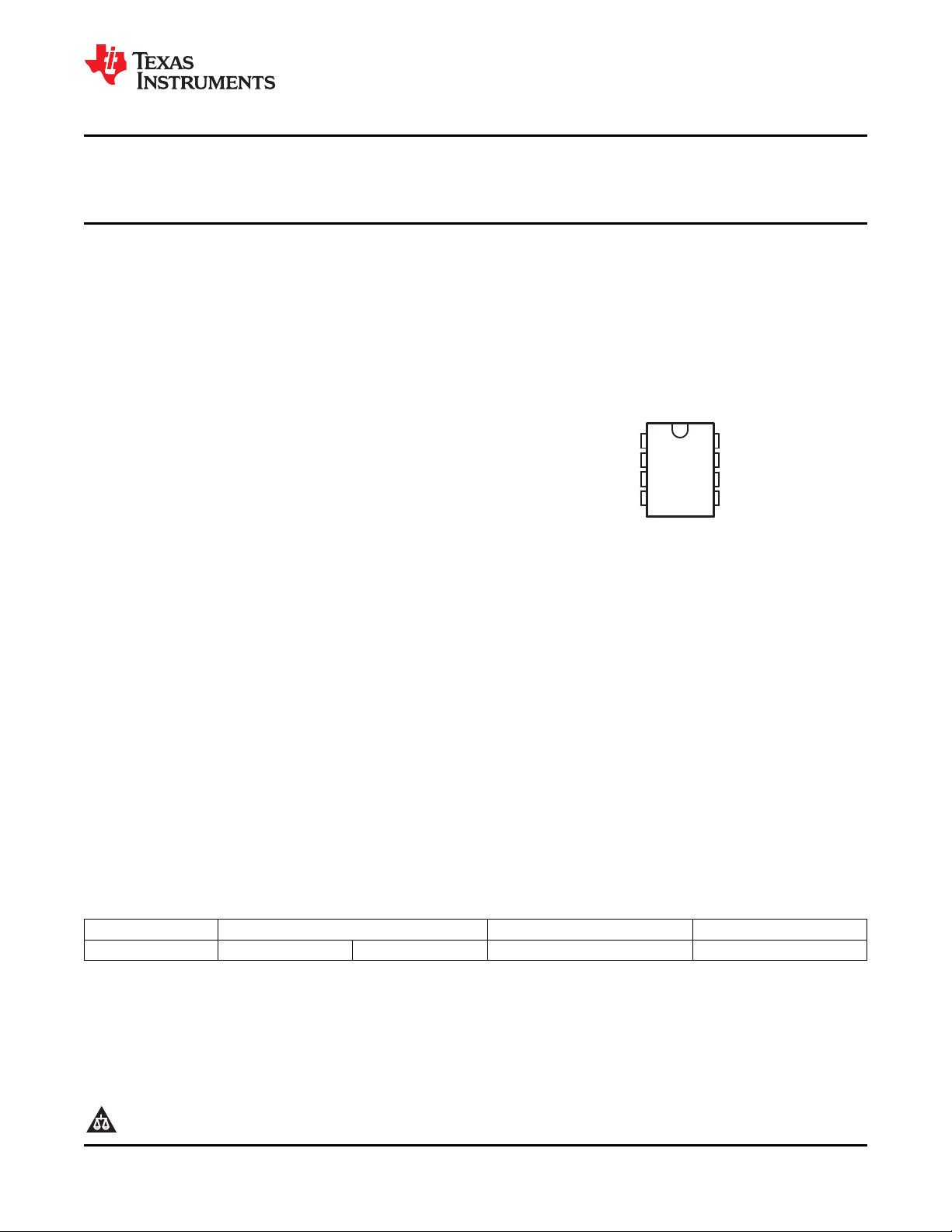
DCU PACKAGE
(TOP VIEW)
1
2
3
4
8
7
6
5
V
CCA
A1
A2
GND
V
CCB
B1
B2
DIR
SN74AVC2T45-Q1
www.ti.com
SCES813 –JUNE 2010
DUAL-BIT DUAL-SUPPLY BUS TRANSCEIVER
WITH CONFIGURABLE VOLTAGE TRANSLATION AND 3-STATE OUTPUTS
Check for Samples: SN74AVC2T45-Q1
1
FEATURES
• Qualified for Automotive Applications
• Control Inputs VIH/VILLevels Are Referenced to
V
Voltage – 8000-V Human-Body Model (A114-A)
CCA
• Fully Configurable Dual-Rail Design Allows – 200-V Machine Model (A115-A)
Each Port to Operate Over the Full 1.2-V to
3.6-V Power-Supply Range
• I/Os Are 4.6-V Tolerant
• I
Supports Partial-Power-Down Mode
off
Operation
• Max Data Rates
– 500 Mbps (1.8-V to 3.3-V Translation)
– 320 Mbps (<1.8-V to 3.3-V Translation)
– 320 Mbps (Translate to 2.5 V or 1.8 V)
– 280 Mbps (Translate to 1.5 V)
– 240 Mbps (Translate to 1.2 V)
• Latch-Up Performance Exceeds 100 mA Per
JESD 78, Class II
• ESD Protection Exceeds JESD 22
– 1000-V Charged-Device Model (C101)
DESCRIPTION
This dual-bit noninverting bus transceiver uses two separate configurable power-supply rails. The A port is
designed to track V
V
CCB
. V
accepts any supply voltage from 1.2 V to 3.6 V. This allows for universal low-voltage bidirectional
CCB
translation between any of the 1.2-V, 1.5-V, 1.8-V, 2.5-V, and 3.3-V voltage nodes.
The SN74AVC2T45 is designed for asynchronous communication between two data buses. The logic levels of
the direction-control (DIR) input activate either the B-port outputs or the A-port outputs. The device transmits data
from the A bus to the B bus when the B-port outputs are activated and from the B bus to the A bus when the
A-port outputs are activated. The input circuitry on both A and B ports always is active and must have a logic
HIGH or LOW level applied to prevent excess ICCand I
The SN74AVC2T45 is designed so that the DIR input is powered by V
This device is fully specified for partial-power-down applications using I
preventing damaging current backflow through the device when it is powered down.
The VCCisolation feature ensures that if either VCCinput is at GND, both ports are in the high-impedance state.
T
A
–40°C to 105°C VSSOP – DCU Reel of 3000 CAVC2T45TDCURQ1 SBUI
(1) For the most current package and ordering information, see the Package Option Addendum at the end of this document, or see the TI
web site at www.ti.com.
(2) Package drawings, thermal data, and symbolization are available at www.ti.com/packaging.
CCA
. V
accepts any supply voltage from 1.2 V to 3.6 V. The B port is designed to track
CCA
.
CCZ
.
CCA
PACKAGE
ORDERING INFORMATION
(2)
ORDERABLE PART NUMBER TOP-SIDE MARKING
(1)
. The I
off
circuitry disables the outputs,
off
1
PRODUCTION DATA information is current as of publication date.
Products conform to specifications per the terms of the Texas
Instruments standard warranty. Production processing does not
necessarily include testing of all parameters.
Please be aware that an important notice concerning availability, standard warranty, and use in critical applications of Texas
Instruments semiconductor products and disclaimers thereto appears at the end of this data sheet.
Copyright © 2010, Texas Instruments Incorporated
Page 2
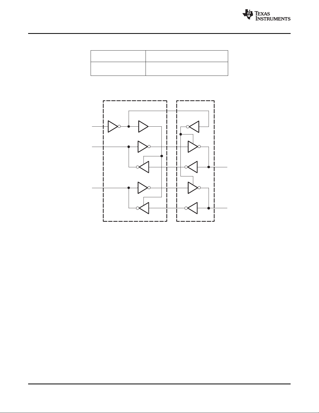
B1
DIR
5
7
A1
2
V
CCA
V
CCB
B2
6
A2
3
SN74AVC2T45-Q1
SCES813 –JUNE 2010
FUNCTION TABLE
(1)
(EACH TRANSCEIVER)
INPUT
DIR
L B data to A bus
H A data to B bus
(1) Input circuits of the data I/Os always are active.
OPERATION
LOGIC DIAGRAM (POSITIVE LOGIC)
www.ti.com
2 Submit Documentation Feedback Copyright © 2010, Texas Instruments Incorporated
Product Folder Link(s): SN74AVC2T45-Q1
Page 3
SN74AVC2T45-Q1
www.ti.com
ABSOLUTE MAXIMUM RATINGS
(1)
SCES813 –JUNE 2010
over operating free-air temperature range (unless otherwise noted)
MIN MAX UNIT
V
CCA
V
CCB
V
I
V
O
V
O
I
IK
I
OK
I
O
q
JA
T
stg
(1) Stresses beyond those listed under "absolute maximum ratings" may cause permanent damage to the device. These are stress ratings
(2) The input negative-voltage and output voltage ratings may be exceeded if the input and output current ratings are observed.
(3) The output positive-voltage rating may be exceeded up to 4.6 V maximum if the output current ratings are observed.
(4) The package thermal impedance is calculated in accordance with JESD 51-7.
Supply voltage range –0.5 4.6 V
I/O ports (A port) –0.5 4.6
Input voltage range
(2)
I/O ports (B port) –0.5 4.6 V
Control inputs –0.5 4.6
Voltage range applied to any output in the high-impedance or
power-off state
(2)
Voltage range applied to any output in the high or low state
(2) (3)
A port –0.5 4.6
B port –0.5 4.6
A port –0.5 V
B port –0.5 V
CCA
CCB
+ 0.5
+ 0.5
Input clamp current VI< 0 –50 mA
Output clamp current VO< 0 –50 mA
Continuous output current ±50 mA
Continuous current through V
Package thermal impedance
(4)
CCA
, V
, or GND ±100 mA
CCB
DCU package 227 °C/W
Storage temperature range –65 150 °C
only, and functional operation of the device at these or any other conditions beyond those indicated under "recommended operating
conditions" is not implied. Exposure to absolute-maximum-rated conditions for extended periods may affect device reliability.
V
V
Copyright © 2010, Texas Instruments Incorporated Submit Documentation Feedback 3
Product Folder Link(s): SN74AVC2T45-Q1
Page 4
SN74AVC2T45-Q1
SCES813 –JUNE 2010
RECOMMENDED OPERATING CONDITIONS
V
CCA
V
CCB
V
IH
Supply voltage 1.2 3.6 V
Supply voltage 1.2 3.6 V
High-level
input voltage
Data inputs
(4)
(1)(2)(3)(4)(5)
V
CCI
1.2 V to 1.95 V V
V
CCO
MIN MAX UNIT
× 0.65
CCI
1.95 V to 2.7 V 1.6 V
www.ti.com
2.7 V to 3.6 V 2
V
IL
Low-level
input voltage
Data inputs
(4)
1.95 V to 2.7 V 0.7 V
1.2 V to 1.95 V V
CCI
× 0.35
2.7 V to 3.6 V 0.8
V
IH
High-level DIR
input voltage (referenced to V
CCA
(5)
)
1.95 V to 2.7 V 1.6 V
2.7 V to 3.6 V 2
1.2 V to 1.95 V V
1.2 V to 1.95 V V
V
IL
V
I
V
O
Low-level DIR
input voltage (referenced to V
CCA
(5)
)
1.95 V to 2.7 V 0.7 V
2.7 V to 3.6 V 0.8
Input voltage 0 3.6 V
Output voltage V
Active state 0 V
3-state 0 3.6
CCA
× 0.65
CCA
× 0.35
CCO
1.2 V –3
1.4 V to 1.6 V –6
I
OH
High-level output current 1.65 V to 1.95 V –8 mA
2.3 V to 2.7 V –9
3 V to 3.6 V –12
1.2 V 3
1.4 V to 1.6 V 6
I
OL
Low-level output current 1.65 V to 1.95 V 8 mA
2.3 V to 2.7 V 9
3 V to 3.6 V 12
Δt/Δv Input transition rise or fall rate 5 ns/V
T
A
(1) V
(2) V
(3) All unused data inputs of the device must be held at V
(4) For V
(5) For V
Operating free-air temperature –40 105 °C
is the VCCassociated with the input port.
CCI
is the VCCassociated with the output port.
CCO
Implications of Slow or Floating CMOS Inputs, literature number SCBA004.
values not specified in the data sheet, VIHmin = V
CCI
values not specified in the data sheet, VIHmin = V
CCI
or GND to ensure proper device operation. See the TI application report,
CCI
× 0.7 V, VILmax = V
CCI
× 0.7 V, VILmax = V
CCA
CCI
CCA
× 0.3 V.
× 0.3 V.
4 Submit Documentation Feedback Copyright © 2010, Texas Instruments Incorporated
Product Folder Link(s): SN74AVC2T45-Q1
Page 5

SN74AVC2T45-Q1
www.ti.com
ELECTRICAL CHARACTERISTICS
(1)(2)
over recommended operating free-air temperature range (unless otherwise noted)
PARAMETER TEST CONDITIONS V
CCA
V
CCB
IOH= –100 mA 1.2 V to 3.6 V 1.2 V to 3.6 V V
IOH= –3 mA 1.2 V 1.2 V 0.95
V
OH
IOH= –6 mA 1.4 V 1.4 V 1.05
IOH= –8 mA 1.65 V 1.65 V 1.2
VI= V
IH
IOH= –9 mA 2.3 V 2.3 V 1.75
IOH= –12 mA 3 V 3 V 2.3
IOL= 100 mA 1.2 V to 3.6 V 1.2 V to 3.6 V 0.2
IOL= 3 mA 1.2 V 1.2 V 0.25
V
OL
IOL= 6 mA 1.4 V 1.4 V 0.35
IOL= 8 mA 1.65 V 1.65 V 0.45
VI= V
IL
IOL= 9 mA 2.3 V 2.3 V 0.55
IOL= 12 mA 3 V 3 V 0.7
I
DIR VI= V
I
A port 0 V 0 to 3.6 V ±0.1 ±1 ±5
I
off
B port 0 to 3.6 V 0 V ±0.1 ±1 ±5
B port 0 V 3.6 V ±0.5 ±2.5 ±5
I
OZ
A port 3.6 V 0 V ±0.5 ±2.5 ±5
VIor VO= 0 to 3.6 V mA
VO= V
VI= V
or GND 1.2 V to 3.6 V 1.2 V to 3.6 V ±0.025 ±0.25 ±1 mA
CCA
or GND,
CCO
or GND
CCI
1.2 V to 3.6 V 1.2 V to 3.6 V 10
I
CCA
VI= V
or GND, IO= 0 0 V 3.6 V –2 mA
CCI
3.6 V 0 V 10
1.2 V to 3.6 V 1.2 V to 3.6 V 10
I
CCB
VI= V
or GND, IO= 0 0 V 3.6 V 10 mA
CCI
3.6 V 0 V –2
I
+ I
CCA
CCB
(see Table 1)
Control
C
I
inputs
A or B
C
io
port
(1) V
CCO
(2) V
CCI
VI= V
or GND, IO= 0 1.2 V to 3.6 V 1.2 V to 3.6 V 20 mA
CCI
VI= 3.3 V or GND 3.3 V 3.3 V 2.5 pF
VO= 3.3 V or GND 3.3 V 3.3 V 6 pF
is the VCCassociated with the output port.
is the VCCassociated with the input port.
TA= 25°C –40°C to 105°C
MIN TYP MAX MIN MAX
CCO
SCES813 –JUNE 2010
UNIT
– 0.2 V
V
V
mA
Copyright © 2010, Texas Instruments Incorporated Submit Documentation Feedback 5
Product Folder Link(s): SN74AVC2T45-Q1
Page 6
SN74AVC2T45-Q1
SCES813 –JUNE 2010
www.ti.com
SWITCHING CHARACTERISTICS
over recommended operating free-air temperature range, V
V
= 1.2 V V
PARAMETER UNIT
t
PLH
t
PHL
t
PLH
t
PHL
t
PHZ
t
PLZ
t
PHZ
t
PLZ
(1)
t
PZH
(1)
t
PZL
(1)
t
PZH
(1)
t
PZL
FROM TO
(INPUT) (OUTPUT)
A B ns
B A ns
DIR A ns
DIR B ns
DIR A ns
DIR B ns
(1) The enable time is a calculated value, derived using the formula shown in the enable times section.
CCB
TYP TYP TYP TYP TYP
3.1 2.6 2.4 2.2 2.2
3.1 2.6 2.4 2.2 2.2
3.4 3.1 3 2.9 2.9
3.4 3.1 3 2.9 2.9
5.2 5.2 5.1 5 4.8
5.2 5.2 5.1 5 4.8
5 4 3.8 2.8 3.2
5 4 3.8 2.8 3.2
8.4 7.1 6.8 5.7 6.1
8.4 7.1 6.8 5.7 6.1
8.3 7.8 7.5 7.2 7
8.3 7.8 7.5 7.2 7
= 1.2 V (see Figure 1)
CCA
= 1.5 V V
CCB
= 1.8 V V
CCB
= 2.5 V V
CCB
CCB
= 3.3 V
SWITCHING CHARACTERISTICS
over recommended operating free-air temperature range, V
V
= 1.2 V
PARAMETER UNIT
t
PLH
t
PHL
t
PLH
t
PHL
t
PHZ
t
PLZ
t
PHZ
t
PLZ
(1)
t
PZH
(1)
t
PZL
(1)
t
PZH
(1)
t
PZL
FROM TO
(INPUT) (OUTPUT)
A B ns
B A ns
DIR A ns
DIR B ns
DIR A ns
DIR B ns
(1) The enable time is a calculated value, derived using the formula shown in the enable times section.
CCB
TYP MIN MAX MIN MAX MIN MAX MIN MAX
2.8 0.7 5.6 0.5 4.8 0.4 3.9 0.3 3.7
2.8 0.7 5.6 0.5 4.8 0.4 3.9 0.3 3.7
2.7 0.8 5.6 0.7 5.4 0.6 5.1 0.5 4.9
2.7 0.8 5.6 0.7 5.4 0.6 5.1 0.5 4.9
3.9 1.3 8.7 1.3 8 1.1 7.9 1.4 7.8
3.9 1.3 8.7 1.3 8 1.1 7.9 1.4 7.8
4.7 1.1 7.2 1.4 7.1 1.2 7.1 1.7 7.3
4.7 1.1 7.2 1.4 7.1 1.2 7.1 1.7 7.3
7.4 12.6 12.3 12 12
7.4 12.6 12.3 12 12
6.7 14.1 12.6 11.6 11.3
6.7 14.1 12.6 11.6 11.3
= 1.5 V ± 0.1 V (see Figure 1)
CCA
V
= 1.5 V V
CCB
± 0.1 V ± 0.15 V ± 0.2 V ± 0.3 V
= 1.8 V V
CCB
= 2.5 V V
CCB
CCB
= 3.3 V
6 Submit Documentation Feedback Copyright © 2010, Texas Instruments Incorporated
Product Folder Link(s): SN74AVC2T45-Q1
Page 7
SN74AVC2T45-Q1
www.ti.com
SCES813 –JUNE 2010
SWITCHING CHARACTERISTICS
over recommended operating free-air temperature range, V
V
= 1.2 V
PARAMETER UNIT
t
PLH
t
PHL
t
PLH
t
PHL
t
PHZ
t
PLZ
t
PHZ
t
PLZ
(1)
t
PZH
(1)
t
PZL
(1)
t
PZH
(1)
t
PZL
FROM TO
(INPUT) (OUTPUT)
A B ns
B A ns
DIR A ns
DIR B ns
DIR A ns
DIR B ns
(1) The enable time is a calculated value, derived using the formula shown in the enable times section.
CCB
TYP MIN MAX MIN MAX MIN MAX MIN MAX
2.7 0.5 5.4 0.4 4.5 0.2 3.6 0.2 3.3
2.7 0.5 5.4 0.4 4.5 0.2 3.6 0.2 3.3
2.4 0.7 4.9 0.5 4.6 0.5 4.2 0.4 4
2.4 0.7 4.9 0.5 4.6 0.5 4.2 0.4 4
3.7 1.3 8.3 0.7 7.1 1.4 5.5 1.1 5.4
3.7 1.3 8.3 0.7 7.1 1.4 5.5 1.1 5.4
4.4 1.3 6 1.3 6.1 0.8 5.9 1.5 6.1
4.4 1.3 6 1.3 6.1 0.8 5.9 1.5 6.1
6.8 10.7 10.5 9.9 9.9
6.8 10.7 10.5 9.9 9.9
6.4 13.5 11.4 8.9 8.5
6.4 13.5 11.4 8.9 8.5
= 1.8 V ± 0.15 V (see Figure 1)
CCA
V
= 1.5 V V
CCB
± 0.1 V ± 0.15 V ± 0.2 V ± 0.3 V
= 1.8 V V
CCB
= 2.5 V V
CCB
CCB
= 3.3 V
SWITCHING CHARACTERISTICS
over recommended operating free-air temperature range, V
V
= 1.2 V
PARAMETER UNIT
t
PLH
t
PHL
t
PLH
t
PHL
t
PHZ
t
PLZ
t
PHZ
t
PLZ
(1)
t
PZH
(1)
t
PZL
(1)
t
PZH
(1)
t
PZL
FROM TO
(INPUT) (OUTPUT)
A B ns
B A ns
DIR A ns
DIR B ns
DIR A ns
DIR B ns
(1) The enable time is a calculated value, derived using the formula shown in the enable times section.
CCB
TYP MIN MAX MIN MAX MIN MAX MIN MAX
2.6 0.4 5.1 0.2 4.2 0.2 3.2 0.2 2.8
2.6 0.4 5.1 0.2 4.2 0.2 3.2 0.2 2.8
2.1 0.6 4 0.5 3.6 0.4 3.2 0.3 3
2.1 0.6 4 0.5 3.6 0.4 3.2 0.3 3
2.4 0.7 8.1 0.8 6.6 0.8 5.2 0.5 4.5
2.4 0.7 8.1 0.8 6.6 0.8 5.2 0.5 4.5
3.8 1 4.5 0.6 4.5 0.5 4.4 1.1 4.3
3.8 1 4.5 0.6 4.5 0.5 4.4 1.1 4.3
5.9 8.7 7.9 7.4 7.1
5.9 8.7 7.9 7.4 7.1
5 13 10.6 8.2 7.1
5 13 10.6 8.2 7.1
= 2.5 V ± 0.2 V (see Figure 1)
CCA
V
= 1.5 V V
CCB
± 0.1 V ± 0.15 V ± 0.2 V ± 0.3 V
= 1.8 V V
CCB
= 2.5 V V
CCB
CCB
= 3.3 V
Copyright © 2010, Texas Instruments Incorporated Submit Documentation Feedback 7
Product Folder Link(s): SN74AVC2T45-Q1
Page 8

SN74AVC2T45-Q1
SCES813 –JUNE 2010
www.ti.com
SWITCHING CHARACTERISTICS
over recommended operating free-air temperature range, V
V
= 1.2 V
PARAMETER UNIT
t
PLH
t
PHL
t
PLH
t
PHL
t
PHZ
t
PLZ
t
PHZ
t
PLZ
(1)
t
PZH
(1)
t
PZL
(1)
t
PZH
(1)
t
PZL
FROM TO
(INPUT) (OUTPUT)
A B ns
B A ns
DIR A ns
DIR B ns
DIR A ns
DIR B ns
(1) The enable time is a calculated value, derived using the formula shown in the enable times section.
CCB
TYP MIN MAX MIN MAX MIN MAX MIN MAX
2.5 0.3 4.9 0.2 4 0.2 3 0.2 2.6
2.5 0.3 4.9 0.2 4 0.2 3 0.2 2.6
2.1 0.6 3.8 0.4 3.3 0.3 2.8 0.3 2.6
2.1 0.6 3.8 0.4 3.3 0.3 2.8 0.3 2.6
2.9 1.1 8.2 1 6.7 1.3 4.9 1.2 4.2
2.9 1.1 8.2 1 6.7 1.3 4.9 1.2 4.2
3.4 0.5 6.8 0.3 5.8 0.3 4.8 1.1 4.4
3.4 0.5 6.8 0.3 5.8 0.3 4.8 1.1 4.4
5.5 10.4 8.9 7.4 6.8
5.5 10.4 8.9 7.4 6.8
5.4 12.9 10.5 7.7 6.6
5.4 12.9 10.5 7.7 6.6
= 3.3 V ± 0.3 V (see Figure 1)
CCA
V
= 1.5 V V
CCB
± 0.1 V ± 0.15 V ± 0.2 V ± 0.3 V
= 1.8 V V
CCB
= 2.5 V V
CCB
CCB
= 3.3 V
OPERATING CHARACTERISTICS
TA= 25°C
V
= V
PARAMETER UNIT
A-port input,
pdA
B-port input,
B-port output
(1)
C
A-port output
A-port input,
pdB
B-port input,
B-port output
(1)
C
A-port output
TEST
CONDITIONS
CL= 0,
f = 10 MHz, pF
tr= tf= 1 ns
CL= 0,
f = 10 MHz, pF
tr= tf= 1 ns
CCA
V
= 1.2 V V
CCB
TYP TYP TYP TYP TYP
3 3 3 3 4
12 13 13 14 15
12 13 13 14 15
3 3 3 3 4
(1) Power-dissipation capacitance per transceiver
CCA
= 1.5 V V
CCB
= V
CCB
= V
CCA
= 1.8 V V
CCA
= 2.5 V V
CCB
= V
CCB
CCA
= 3.3 V
=
8 Submit Documentation Feedback Copyright © 2010, Texas Instruments Incorporated
Product Folder Link(s): SN74AVC2T45-Q1
Page 9

SN74AVC2T45-Q1
www.ti.com
SCES813 –JUNE 2010
Power-Up Considerations
A proper power-up sequence always should be followed to avoid excessive supply current, bus contention,
oscillations, or other anomalies. To guard against such power-up problems, take the following precautions:
1. Connect ground before any supply voltage is applied.
2. Power up V
3. V
can be ramped up along with or after V
CCB
.
CCA
.
CCA
Table 1. Typical Total Static Power Consumption (I
V
V
CCB
0 V 0 <0.5 <0.5 <0.5 <0.5 <0.5
1.2 V <0.5 <1 <1 <1 <1 1
1.5 V <0.5 <1 <1 <1 <1 1
1.8 V <0.5 <1 <1 <1 <1 <1
2.5 V <0.5 1 <1 <1 <1 <1
3.3 V <0.5 1 <1 <1 <1 <1
0 V 1.2 V 1.5 V 1.8 V 2.5 V 3.3 V
CCA
CCA
+ I
CCB
)
UNIT
mA
Copyright © 2010, Texas Instruments Incorporated Submit Documentation Feedback 9
Product Folder Link(s): SN74AVC2T45-Q1
Page 10

t
PHL
- ns
CL - pF
0
1
2
3
4
5
6
0 10 20 30 40 50 60
V
CCB
= 1.8 V
V
CCB
= 2.5 V
V
CCB
= 3.3 V
V
CCB
= 1.5 V
V
CCB
= 1.2 V
0
1
2
3
4
5
6
0 10 20 30 40 50
t
PLH
- ns
C
L
- pF
60
V
CCB
= 1.8 V
V
CCB
= 2.5 V
V
CCB
= 3.3 V
V
CCB
= 1.5 V
V
CCB
= 1.2 V
t
PHL
- ns
CL - pF
0
1
2
3
4
5
6
0 10 20 30 40 50 60
V
CCB
= 1.8 V
V
CCB
= 2.5 V
V
CCB
= 3.3 V
V
CCB
= 1.5 V
V
CCB
= 1.2 V
0
1
2
3
4
5
6
0 10 20 30 40 50
t
PLH
- ns
C
L
- pF
60
V
CCB
= 1.8 V
V
CCB
= 2.5 V
V
CCB
= 3.3 V
V
CCB
= 1.5 V
V
CCB
= 1.2 V
SN74AVC2T45-Q1
SCES813 –JUNE 2010
TYPICAL CHARACTERISTICS
TYPICAL PROPAGATION DELAY (A to B) vs LOAD CAPACITANCE,
TA= 25°C, V
CCA
= 1.2 V
www.ti.com
TYPICAL PROPAGATION DELAY (A to B) vs LOAD CAPACITANCE,
TA= 25°C, V
CCA
= 1.5 V
10 Submit Documentation Feedback Copyright © 2010, Texas Instruments Incorporated
Product Folder Link(s): SN74AVC2T45-Q1
Page 11

0
1
2
3
4
5
6
0 10 20 30 40 50 60
t
PHL
- ns
CL - pF
V
CCB
= 1.8 V
V
CCB
= 2.5 V
V
CCB
= 3.3 V
V
CCB
= 1.5 V
V
CCB
= 1.2 V
0
1
2
3
4
5
6
0 10 20 30 40 50
t
PLH
- ns
C
L
- pF
60
V
CCB
= 1.8 V
V
CCB
= 2.5 V
V
CCB
= 3.3 V
V
CCB
= 1.5 V
V
CCB
= 1.2 V
t
PHL
- ns
CL - pF
0
1
2
3
4
5
6
0 10 20 30 40 50 60
V
CCB
= 1.8 V
V
CCB
= 2.5 V
V
CCB
= 3.3 V
V
CCB
= 1.5 V
V
CCB
= 1.2 V
0
1
2
3
4
5
6
0 10 20 30 40 50
t
PLH
- ns
C
L
- pF
60
V
CCB
= 1.8 V
V
CCB
= 2.5 V
V
CCB
= 3.3 V
V
CCB
= 1.5 V
V
CCB
= 1.2 V
SN74AVC2T45-Q1
www.ti.com
TYPICAL CHARACTERISTICS (continued)
TYPICAL PROPAGATION DELAY (A to B) vs LOAD CAPACITANCE,
TA= 25°C, V
CCA
= 1.8 V
SCES813 –JUNE 2010
TYPICAL PROPAGATION DELAY (A to B) vs LOAD CAPACITANCE,
TA= 25°C, V
CCA
= 2.5 V
Copyright © 2010, Texas Instruments Incorporated Submit Documentation Feedback 11
Product Folder Link(s): SN74AVC2T45-Q1
Page 12

t
PHL
- ns
CL - pF
0
1
2
3
4
5
6
0 10 20 30 40 50 60
V
CCB
= 1.8 V
V
CCB
= 2.5 V
V
CCB
= 3.3 V
V
CCB
= 1.5 V
V
CCB
= 1.2 V
0
1
2
3
4
5
6
0 10 20 30 40 50
t
PLH
- ns
C
L
- pF
60
V
CCB
= 1.8 V
V
CCB
= 2.5 V
V
CCB
= 3.3 V
V
CCB
= 1.5 V
V
CCB
= 1.2 V
SN74AVC2T45-Q1
SCES813 –JUNE 2010
TYPICAL CHARACTERISTICS (continued)
TYPICAL PROPAGATION DELAY (A to B) vs LOAD CAPACITANCE,
TA= 25°C, V
CCA
= 3.3 V
www.ti.com
12 Submit Documentation Feedback Copyright © 2010, Texas Instruments Incorporated
Product Folder Link(s): SN74AVC2T45-Q1
Page 13

V
OH
V
OL
From Output
Under Test
C
L
(see Note A)
LOAD CIRCUIT
S1
2 × V
CCO
Open
GND
R
L
R
L
t
PLH
t
PHL
Output
Control
(low-level
enabling)
Output
Waveform 1
S1 at 2 × V
CCO
(see Note B)
Output
Waveform 2
S1 at GND
(see Note B)
t
PZL
t
PZH
t
PLZ
t
PHZ
V
CCA
/2V
CCA
/2
V
CCI
/2 V
CCI
/2
V
CCI
0 V
V
CCO
/2 V
CCO
/2
V
OH
V
OL
0 V
V
CCO
/2
VOL + V
TP
V
CCO
/2
VOH - V
TP
0 V
V
CCI
0 V
V
CCI
/2 V
CCI
/2
t
w
Input
V
CCA
V
CCO
VOLTAGE WAVEFORMS
PROPAGATION DELAY TIMES
VOLTAGE WAVEFORMS
PULSE DURATION
VOLTAGE WAVEFORMS
ENABLE AND DISABLE TIMES
Output
Input
t
pd
t
PLZ/tPZL
t
PHZ/tPZH
Open
2 × V
CCO
GND
TEST S1
NOTES: A. CL includes probe and jig capacitance.
B. Waveform 1 is for an output with internal conditions such that the output is low, except when disabled by the output control.
Waveform2 is for an output with internal conditions such that the output is high, except when disabled by the output control.
C. All input pulses are supplied by generators having the following characteristics: PRRv10 MHz, ZO = 50 Ω, dv/dt ≥ 1 V/ns.
D. The outputs are measured one at a time, with one transition per measurement.
E. t
PLZ
and t
PHZ
are the same as t
dis
.
F. t
PZL
and t
PZH
are the same as ten.
G. t
PLH
and t
PHL
are the same as tpd.
H. V
CCI
is the VCC associated with the input port.
I. V
CCO
is the VCC associated with the output port.
1.2 V
1.5 V ± 0.1 V
1.8 V ± 0.15 V
2.5 V ± 0.2 V
3.3 V ± 0.3 V
2 kΩ
2 kΩ
2 kΩ
2 kΩ
2 kΩ
V
CCO
R
L
0.1 V
0.1 V
0.15 V
0.15 V
0.3 V
V
TP
C
L
15 pF
15 pF
15 pF
15 pF
15 pF
SN74AVC2T45-Q1
www.ti.com
SCES813 –JUNE 2010
PARAMETER MEASUREMENT INFORMATION
Figure 1. Load Circuit and Voltage Waveforms
Copyright © 2010, Texas Instruments Incorporated Submit Documentation Feedback 13
Product Folder Link(s): SN74AVC2T45-Q1
Page 14

V
CC1
V
CC1
V
CC2
SYSTEM-1 SYSTEM-2
V
CC1
1
2
3
4
8
7
6
5
V
CC2
V
CC2
SN74AVC2T45-Q1
SCES813 –JUNE 2010
www.ti.com
APPLICATION INFORMATION
Figure 2 is an example circuit of the SN74AVC2T45 used in a unidirectional logic level-shifting application.
PIN NAME FUNCTION DESCRIPTION
1 V
CCA
2 A1 OUT1 Output level depends on V
3 A2 OUT2 Output level depends on V
4 GND GND Device GND
5 DIR DIR The GND (low-level) determines B-port to A-port direction.
6 B2 IN2 Input threshold value depends on V
7 B1 IN1 Input threshold value depends on V
8 V
CCB
V
CC1
V
CC2
SYSTEM-1 supply voltage (1.2 V to 3.6 V)
voltage.
CC1
voltage.
CC1
voltage.
CC2
voltage.
CC2
SYSTEM-2 supply voltage (1.2 V to 3.6 V)
Figure 2. Unidirectional Logic Level-Shifting Application
14 Submit Documentation Feedback Copyright © 2010, Texas Instruments Incorporated
Product Folder Link(s): SN74AVC2T45-Q1
Page 15

V
CC1
V
CC1
V
CC2
SYSTEM-1 SYSTEM-2
1
2
3
4
8
7
6
5
DIR CTRL
I/O-1
Pullup/Pulldown
or Bus Hold
(1)
V
CC2
I/O-2
Pullup/Pulldown
or Bus Hold
(1)
SN74AVC2T45-Q1
www.ti.com
SCES813 –JUNE 2010
APPLICATION INFORMATION
Figure 3 shows the SN74AVC2T45 used in a bidirectional logic level-shifting application. Since the
SN74AVC2T45 does not have an output-enable (OE) pin, the system designer should take precautions to avoid
bus contention between SYSTEM-1 and SYSTEM-2 when changing directions.
Following is a sequence that illustrates data transmission from SYSTEM-1 to SYSTEM-2 and then from
SYSTEM-2 to SYSTEM-1.
STATE DIR CTRL I/O-1 I/O-2 DESCRIPTION
1 H Out In SYSTEM-1 data to SYSTEM-2
2 H Hi-Z Hi-Z disabled.
3 L Hi-Z Hi-Z
4 L In Out SYSTEM-2 data to SYSTEM-1
(1) SYSTEM-1 and SYSTEM-2 must use the same conditions, i.e., both pullup or both pulldown.
SYSTEM-2 is getting ready to send data to SYSTEM-1. I/O-1 and I/O-2 are
The bus-line state depends on pullup or pulldown.
DIR bit is flipped. I/O-1 and I/O-2 still are disabled.
The bus-line state depends on pullup or pulldown.
(1)
(1)
Figure 3. Bidirectional Logic Level-Shifting Application
Enable Times
Calculate the enable times for the SN74AVC2T45 using the following formulas:
• t
• t
• t
• t
In a bidirectional application, these enable times provide the maximum delay from the time the DIR bit is
switched until an output is expected. For example, if the SN74AVC2T45 initially is transmitting from A to B, then
the DIR bit is switched; the B port of the device must be disabled before presenting it with an input. After the B
port has been disabled, an input signal applied to it appears on the corresponding A port after the specified
propagation delay.
(DIR to A) = t
PZH
(DIR to A) = t
PZL
(DIR to B) = t
PZH
(DIR to B) = t
PZL
PLZ
PHZ
PLZ
PHZ
(DIR to B) + t
(DIR to B) + t
(DIR to A) + t
(DIR to A) + t
PLH
PHL
PLH
PHL
(B to A)
(B to A)
(A to B)
(A to B)
Copyright © 2010, Texas Instruments Incorporated Submit Documentation Feedback 15
Product Folder Link(s): SN74AVC2T45-Q1
Page 16

PACKAGE OPTION ADDENDUM
www.ti.com
10-Dec-2020
PACKAGING INFORMATION
Orderable Device Status
CAVC2T45TDCURQ1 ACTIVE VSSOP DCU 8 3000 RoHS & Green NIPDAU Level-1-260C-UNLIM -40 to 125 SBUI
(1)
The marketing status values are defined as follows:
ACTIVE: Product device recommended for new designs.
LIFEBUY: TI has announced that the device will be discontinued, and a lifetime-buy period is in effect.
NRND: Not recommended for new designs. Device is in production to support existing customers, but TI does not recommend using this part in a new design.
PREVIEW: Device has been announced but is not in production. Samples may or may not be available.
OBSOLETE: TI has discontinued the production of the device.
Package Type Package
(1)
Drawing
Pins Package
Qty
Eco Plan
(2)
Lead finish/
Ball material
(6)
MSL Peak Temp
(3)
Op Temp (°C) Device Marking
(4/5)
(2)
RoHS: TI defines "RoHS" to mean semiconductor products that are compliant with the current EU RoHS requirements for all 10 RoHS substances, including the requirement that RoHS substance
do not exceed 0.1% by weight in homogeneous materials. Where designed to be soldered at high temperatures, "RoHS" products are suitable for use in specified lead-free processes. TI may
reference these types of products as "Pb-Free".
RoHS Exempt: TI defines "RoHS Exempt" to mean products that contain lead but are compliant with EU RoHS pursuant to a specific EU RoHS exemption.
Green: TI defines "Green" to mean the content of Chlorine (Cl) and Bromine (Br) based flame retardants meet JS709B low halogen requirements of <=1000ppm threshold. Antimony trioxide based
flame retardants must also meet the <=1000ppm threshold requirement.
(3)
MSL, Peak Temp. - The Moisture Sensitivity Level rating according to the JEDEC industry standard classifications, and peak solder temperature.
(4)
There may be additional marking, which relates to the logo, the lot trace code information, or the environmental category on the device.
(5)
Multiple Device Markings will be inside parentheses. Only one Device Marking contained in parentheses and separated by a "~" will appear on a device. If a line is indented then it is a continuation
of the previous line and the two combined represent the entire Device Marking for that device.
(6)
Lead finish/Ball material - Orderable Devices may have multiple material finish options. Finish options are separated by a vertical ruled line. Lead finish/Ball material values may wrap to two
lines if the finish value exceeds the maximum column width.
Important Information and Disclaimer:The information provided on this page represents TI's knowledge and belief as of the date that it is provided. TI bases its knowledge and belief on information
provided by third parties, and makes no representation or warranty as to the accuracy of such information. Efforts are underway to better integrate information from third parties. TI has taken and
continues to take reasonable steps to provide representative and accurate information but may not have conducted destructive testing or chemical analysis on incoming materials and chemicals.
TI and TI suppliers consider certain information to be proprietary, and thus CAS numbers and other limited information may not be available for release.
In no event shall TI's liability arising out of such information exceed the total purchase price of the TI part(s) at issue in this document sold by TI to Customer on an annual basis.
OTHER QUALIFIED VERSIONS OF SN74AVC2T45-Q1 :
Samples
Addendum-Page 1
Page 17

PACKAGE OPTION ADDENDUM
www.ti.com
Catalog: SN74AVC2T45
•
NOTE: Qualified Version Definitions:
Catalog - TI's standard catalog product
•
10-Dec-2020
Addendum-Page 2
Page 18

PACKAGE MATERIALS INFORMATION
www.ti.com 3-Aug-2017
TAPE AND REEL INFORMATION
*All dimensions are nominal
Device Package
Type
CAVC2T45TDCURQ1 VSSOP DCU 8 3000 180.0 8.4 2.25 3.35 1.05 4.0 8.0 Q3
Package
Drawing
Pins SPQ Reel
Diameter
(mm)
Reel
Width
W1 (mm)
A0
(mm)B0(mm)K0(mm)P1(mm)W(mm)
Pin1
Quadrant
Pack Materials-Page 1
Page 19

PACKAGE MATERIALS INFORMATION
www.ti.com 3-Aug-2017
*All dimensions are nominal
Device Package Type Package Drawing Pins SPQ Length (mm) Width (mm) Height (mm)
CAVC2T45TDCURQ1 VSSOP DCU 8 3000 202.0 201.0 28.0
Pack Materials-Page 2
Page 20

Page 21

Page 22

IMPORTANT NOTICE AND DISCLAIMER
TI PROVIDES TECHNICAL AND RELIABILITY DATA (INCLUDING DATASHEETS), DESIGN RESOURCES (INCLUDING REFERENCE
DESIGNS), APPLICATION OR OTHER DESIGN ADVICE, WEB TOOLS, SAFETY INFORMATION, AND OTHER RESOURCES “AS IS”
AND WITH ALL FAULTS, AND DISCLAIMS ALL WARRANTIES, EXPRESS AND IMPLIED, INCLUDING WITHOUT LIMITATION ANY
IMPLIED WARRANTIES OF MERCHANTABILITY, FITNESS FOR A PARTICULAR PURPOSE OR NON-INFRINGEMENT OF THIRD
PARTY INTELLECTUAL PROPERTY RIGHTS.
These resources are intended for skilled developers designing with TI products. You are solely responsible for (1) selecting the appropriate
TI products for your application, (2) designing, validating and testing your application, and (3) ensuring your application meets applicable
standards, and any other safety, security, or other requirements. These resources are subject to change without notice. TI grants you
permission to use these resources only for development of an application that uses the TI products described in the resource. Other
reproduction and display of these resources is prohibited. No license is granted to any other TI intellectual property right or to any third
party intellectual property right. TI disclaims responsibility for, and you will fully indemnify TI and its representatives against, any claims,
damages, costs, losses, and liabilities arising out of your use of these resources.
TI’s products are provided subject to TI’s Terms of Sale (www.ti.com/legal/termsofsale.html) or other applicable terms available either on
ti.com or provided in conjunction with such TI products. TI’s provision of these resources does not expand or otherwise alter TI’s applicable
warranties or warranty disclaimers for TI products.
Mailing Address: Texas Instruments, Post Office Box 655303, Dallas, Texas 75265
Copyright © 2020, Texas Instruments Incorporated
 Loading...