

Page 1
SN74ALVCH32374
32-BIT EDGE-TRIGGERED D-TYPE FLIP-FLOP
WITH 3-STATE OUTPUTS
SCES283 – OCTOBER 1999
1
POST OFFICE BOX 655303 • DALLAS, TEXAS 75265
D
Member of the Texas Instruments
Widebus+
Family
D
EPIC
(Enhanced-Performance Implanted
CMOS) Submicron Process
D
Bus Hold on Data Inputs Eliminates the
Need for External Pullup/Pulldown
Resistors
D
Latch-Up Performance Exceeds 100 mA Per
JESD 78, Class II
D
ESD Protection Exceeds JESD 22
– 2000-V Human-Body Model (A114-A)
– 200-V Machine Model (A115-A)
– 1000-V Charged-Device Model (C101)
D
Packaged in Plastic Fine-Pitch Ball Grid
Array Package
description
This 32-bit edge-triggered D-type flip-flop is designed for 1.65-V to 3.6-V VCC operation.
The SN74ALVCH32374 is particularly suitable for implementing buffer registers, I/O ports, bidirectional bus
drivers, and working registers. It can be used as four 8-bit flip-flops, two 16-bit flip-flops, or one 32-bit flip-flop.
On the positive transition of the clock (CLK) input, the Q outputs of the flip-flop take on the logic levels at the
data (D) inputs. The output-enable (OE) input can be used to place the eight outputs in either a normal logic
state (high or low logic levels) or the high-impedance state. In the high-impedance state, the outputs neither
load nor drive the bus lines significantly. The high-impedance state and the increased drive provide the
capability to drive bus lines without need for interface or pullup components.
OE
does not affect internal operations of the flip-flop. Old data can be retained or new data can be entered while
the outputs are in the high-impedance state.
T o ensure the high-impedance state during power up or power down, OE
should be tied to VCC through a pullup
resistor; the minimum value of the resistor is determined by the current-sinking capability of the driver.
Active bus-hold circuitry is provided to hold unused or floating data inputs at a valid logic level.
The SN74ALVCH32374 is characterized for operation from –40°C to 85°C.
FUNCTION TABLE
(each flip-flop)
INPUTS
OUTPUT
OE
CLK D
Q
L ↑ H H
L ↑ LL
L H or L X Q
0
H X X Z
Copyright 1999, Texas Instruments Incorporated
PRODUCTION DATA information is current as of publication date.
Products conform to specifications per the terms of Texas Instruments
standard warranty. Production processing does not necessarily include
testing of all parameters.
Please be aware that an important notice concerning availability, standard warranty, and use in critical applications of
Texas Instruments semiconductor products and disclaimers thereto appears at the end of this data sheet.
EPIC and Widebus+ are trademarks of Texas Instruments Incorporated.
Page 2
SN74ALVCH32374
32-BIT EDGE-TRIGGERED D-TYPE FLIP-FLOP
WITH 3-STATE OUTPUTS
SCES283 – OCTOBER 1999
2
POST OFFICE BOX 655303 • DALLAS, TEXAS 75265
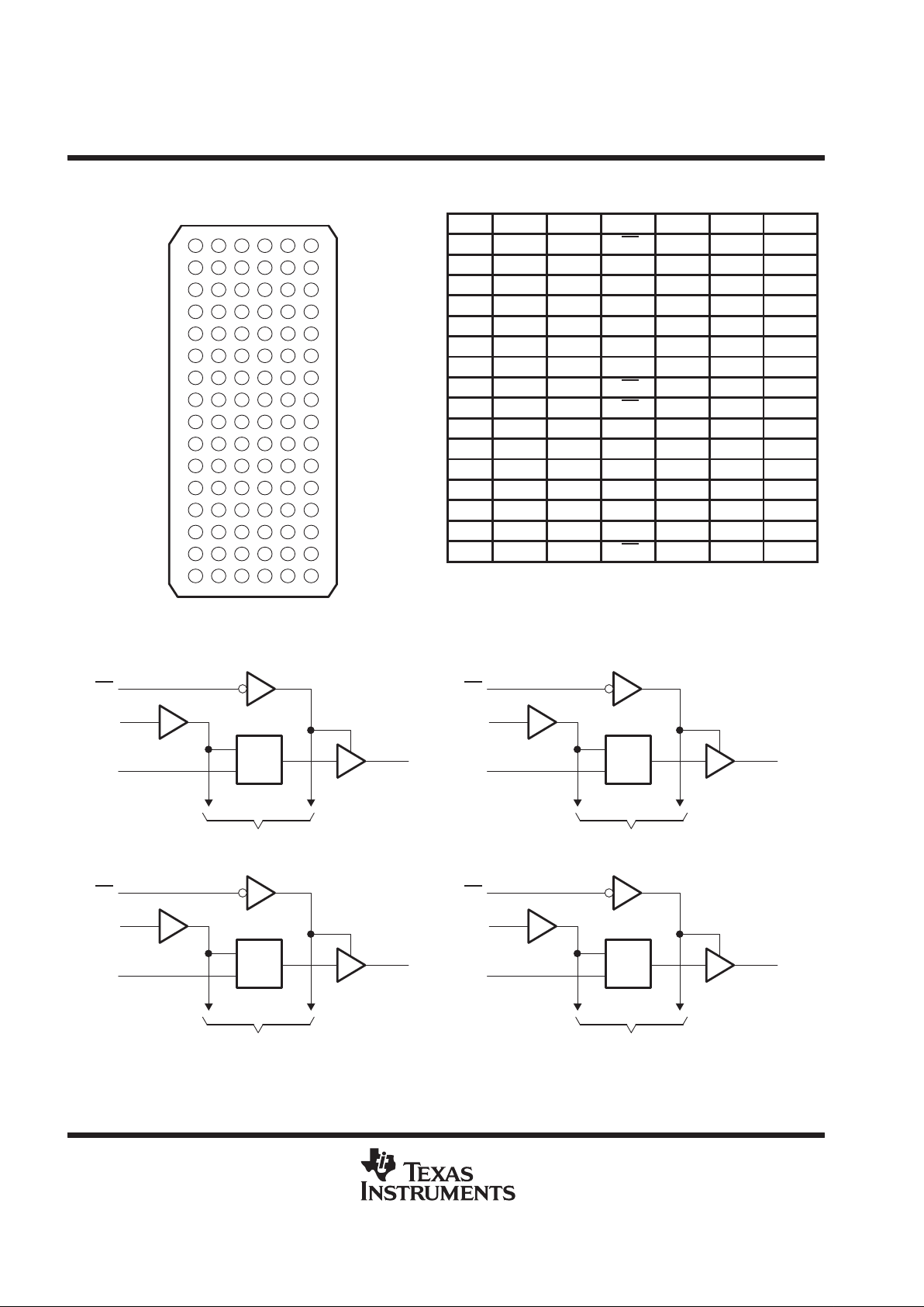
terminal assignments
1 2 3 4 5 6
A 1Q2 1Q1 1OE 1CLK 1D1 1D2
B 1Q4 1Q3 GND GND 1D3 1D4
C 1Q6 1Q5 V
CC
V
CC
1D5 1D6
D 1Q8 1Q7 GND GND 1D7 1D8
E 2Q2 2Q1 GND GND 2D1 2D2
F 2Q4 2Q3 V
CC
V
CC
2D3 2D4
G 2Q6 2Q5 GND GND 2D5 2D6
H 2Q8 2Q7 2OE 2CLK 2D7 2D8
J 3Q2 3Q1 3OE 3CLK 3D1 3D2
K 3Q4 3Q3 GND GND 3D3 3D4
L 3Q6 3Q5 V
CC
V
CC
3D5 3D6
M 3Q8 3Q7 GND GND 3D7 3D8
N 4Q2 4Q1 GND GND 4D1 4D2
P 4Q4 4Q3 V
CC
V
CC
4D3 4D4
R 4Q6 4Q5 GND GND 4D5 4D6
T 4Q7 4Q8 4OE 4CLK 4D8 4D7
logic diagram (positive logic)
1OE
1CLK
1D1
To Seven Other Channels
1Q1
C1
1D
A3
A4
A5
A2
2OE
2CLK
2D1
To Seven Other Channels
2Q1
C1
1D
H3
H4
E5
E2
3OE
3CLK
3D1
To Seven Other Channels
3Q1
C1
1D
J3
J4
J5
J2
4OE
4CLK
4D1
To Seven Other Channels
4Q1
C1
1D
T3
T4
N5
N2
GKE PACKAGE
(TOP VIEW)
A
B
C
D
E
F
G
H
J
K
L
M
N
P
R
T
123456
Page 3
SN74ALVCH32374
32-BIT EDGE-TRIGGERED D-TYPE FLIP-FLOP
WITH 3-STATE OUTPUTS
SCES283 – OCTOBER 1999
3
POST OFFICE BOX 655303 • DALLAS, TEXAS 75265
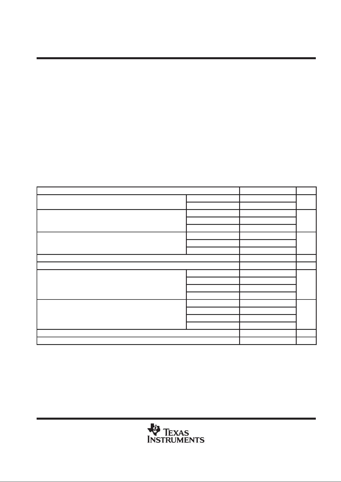
absolute maximum ratings over operating free-air temperature range (unless otherwise noted)
†
Supply voltage range, VCC –0.5 V to 4.6 V. . . . . . . . . . . . . . . . . . . . . . . . . . . . . . . . . . . . . . . . . . . . . . . . . . . . . . . . .
Input voltage range, VI (see Note 1) –0.5 V to 4.6 V. . . . . . . . . . . . . . . . . . . . . . . . . . . . . . . . . . . . . . . . . . . . . . . . .
Output voltage range, V
O
(see Notes 1 and 2) –0.5 V to VCC + 0.5 V. . . . . . . . . . . . . . . . . . . . . . . . . . . . . . . . . .
Input clamp current, IIK (VI < 0) –50 mA. . . . . . . . . . . . . . . . . . . . . . . . . . . . . . . . . . . . . . . . . . . . . . . . . . . . . . . . . . .
Output clamp current, IOK (VO < 0) –50 mA. . . . . . . . . . . . . . . . . . . . . . . . . . . . . . . . . . . . . . . . . . . . . . . . . . . . . . . .
Continuous output current, IO ±50 mA. . . . . . . . . . . . . . . . . . . . . . . . . . . . . . . . . . . . . . . . . . . . . . . . . . . . . . . . . . . . .
Continuous current through each VCC or GND ±100 mA. . . . . . . . . . . . . . . . . . . . . . . . . . . . . . . . . . . . . . . . . . . . .
Package thermal impedance, θ
JA
(see Note 3) 40°C/W. . . . . . . . . . . . . . . . . . . . . . . . . . . . . . . . . . . . . . . . . . . . .
Storage temperature range, T
stg
–65°C to 150°C. . . . . . . . . . . . . . . . . . . . . . . . . . . . . . . . . . . . . . . . . . . . . . . . . . .
†
Stresses beyond those listed under “absolute maximum ratings” may cause permanent damage to the device. These are stress ratings only, and
functional operation of the device at these or any other conditions beyond those indicated under “recommended operating conditions” is not
implied. Exposure to absolute-maximum-rated conditions for extended periods may affect device reliability.
NOTES: 1. The input negative-voltage and output voltage ratings may be exceeded if the input and output current ratings are observed.
2. This value is limited to 4.6 V maximum.
3. The package thermal impedance is calculated in accordance with JESD 51.
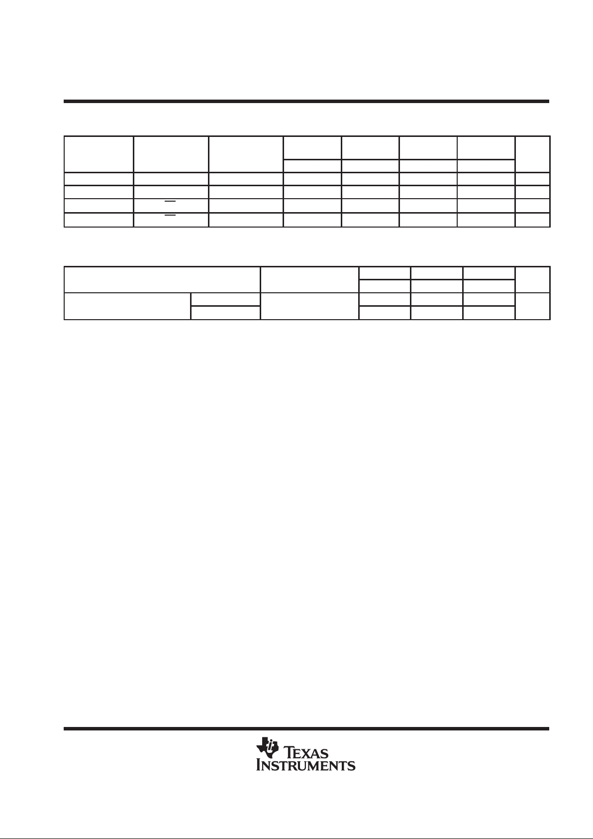
recommended operating conditions (see Note 4)
MIN MAX UNIT
pp
Operating 1.65 3.6
VCCSuppl
y v
oltage
Data retention only 1.5
V
VCC = 1.65 V to 1.95 V 0.65 × V
CC
V
IH
High-level input voltage
VCC = 2.3 V to 2.7 V
1.7
V
VCC = 2.7 V to 3.6 V 2
VCC = 1.65 V to 1.95 V 0.35 × V
CC
V
IL
Low-level input voltage
VCC = 2.3 V to 2.7 V
0.7
V
VCC = 2.7 V to 3.6 V 0.8
V
I
Input voltage 0 V
CC
V
V
O
Output voltage 0 V
CC
V
VCC = 1.65 V –4
p
VCC = 2.3 V –8
IOHHigh-level output current
VCC = 2.7 V –12
mA
VCC = 3 V –24
VCC = 1.65 V 4
p
VCC = 2.3 V 8
IOLLow-level output current
VCC = 2.7 V 12
mA
VCC = 3 V 24
∆t/∆v Input transition rise or fall rate 10 ns/V
T
A
Operating free-air temperature –40 85 °C
NOTE 4: All unused control inputs of the device must be held at VCC or GND to ensure proper device operation. Refer to the TI application report,
Implications of Slow or Floating CMOS Inputs
, literature number SCBA004.
Page 4
SN74ALVCH32374
32-BIT EDGE-TRIGGERED D-TYPE FLIP-FLOP
WITH 3-STATE OUTPUTS
SCES283 – OCTOBER 1999
4
POST OFFICE BOX 655303 • DALLAS, TEXAS 75265
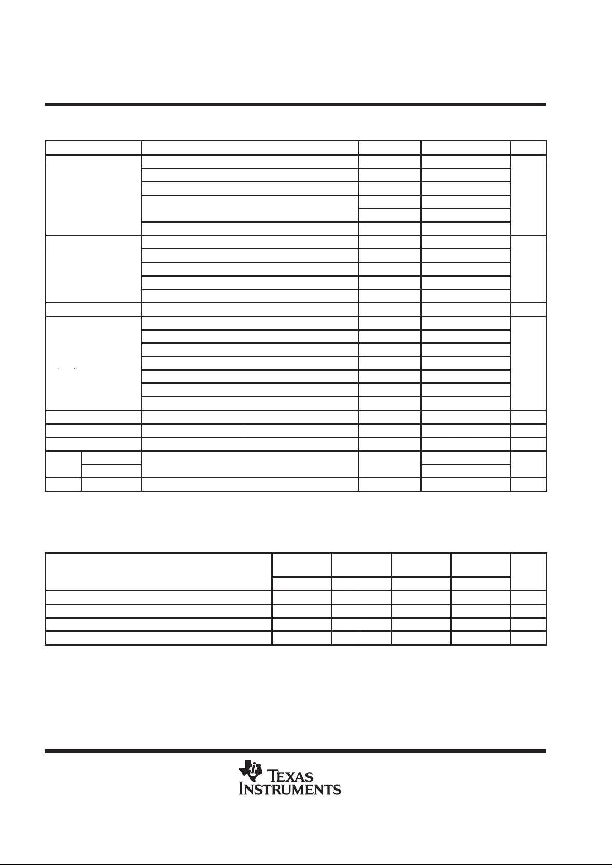
electrical characteristics over recommended operating free-air temperature range (unless
otherwise noted)
PARAMETER TEST CONDITIONS
V
CC
MIN TYP†MAX UNIT
IOH = –100 µA 1.65 V to 3.6 V VCC–0.2
IOH = –4 mA 1.65 V 1.2
IOH = –8 mA 2.3 V 1.7
V
OH
2.7 V 2.2
V
I
OH
= –12
mA
3 V 2.4
IOH = –24 mA 3 V 2.2
IOL = 100 µA 1.65 V to 3.6 V 0.2
IOL = 4 mA 1.65 V 0.45
V
OL
IOL = 8 mA 2.3 V 0.7
V
IOL = 12 mA 2.7 V 0.4
IOL = 24 mA 3 V 0.55
I
I
VI = VCC or GND 3.6 V ±5 µA
VI = 0.58 V 1.65 V 25
VI = 1.07 V 1.65 V –25
VI = 0.7 V 2.3 V 45
I
I(hold)
VI = 1.7 V 2.3 V –45
µA
()
VI = 0.8 V 3 V 75
VI = 2 V 3 V –75
VI = 0 to 3.6 V
‡
3.6 V ±500
I
OZ
VO = VCC or GND 3.6 V ±10 µA
I
CC
VI = VCC or GND, IO = 0 3.6 V 40 µA
∆I
CC
One input at VCC – 0.6 V, Other inputs at VCC or GND 3 V to 3.6 V 750 µA
Control inputs
3
p
C
i
Data inputs
V
I
=
V
CC
or GND
3.3 V
6
pF
C
o
Outputs VO = VCC or GND 3.3 V 7 pF
†
All typical values are at VCC = 3.3 V, TA = 25°C.
‡
This is the bus-hold maximum dynamic current. It is the minimum overdrive current required to switch the input from one state to another.
timing requirements over recommended operating free-air temperature range (unless otherwise
noted) (see Figures 1 through 3)
VCC = 1.8 V
± 0.15 V
VCC = 2.5 V
± 0.2 V
VCC = 2.7 V
VCC = 3.3 V
± 0.3 V
UNIT
MIN MAX MIN MAX MIN MAX MIN MAX
f
clock
Clock frequency
§
150 150 150 MHz
t
w
Pulse duration, CLK high or low
§
3.3 3.3 3.3 ns
t
su
Setup time, data before CLK↑
§
2.1 2.2 1.9 ns
t
h
Hold time, data after CLK↑
§
0.6 0.5 0.5 ns
§
This information was not available at the time of publication.
Page 5
SN74ALVCH32374
32-BIT EDGE-TRIGGERED D-TYPE FLIP-FLOP
WITH 3-STATE OUTPUTS
SCES283 – OCTOBER 1999
5
POST OFFICE BOX 655303 • DALLAS, TEXAS 75265
switching characteristics over recommended operating free-air temperature range (unless
otherwise noted) (see Figures 1 through 3)
PARAMETER
FROM
TO
VCC = 1.8 V
± 0.15 V
VCC = 2.5 V
± 0.2 V
VCC = 2.7 V
VCC = 3.3 V
± 0.3 V
UNIT
(INPUT)
(OUTPUT)
MIN MAX MIN MAX MIN MAX MIN MAX
f
max
†
150 150 150 MHz
t
pd
CLK Q
† †
1 5.3 4.9 1 4.2 ns
t
en
OE
Q
† †
1 6.2 5.9 1 4.8 ns
t
dis
OE
Q
† †
1 5.3 4.7 1.2 4.3 ns
†
This information was not available at the time of publication.
operating characteristics, TA = 25°C
VCC = 1.8 V VCC = 2.5 V VCC = 3.3 V
PARAMETER
TEST CONDITIONS
TYP TYP TYP
UNIT
Power dissipation
Outputs enabled
p
†
31 30
p
C
pd
capacitance
Outputs disabled
C
L
= 50 pF,f = 10 MHz
†
16 18
pF
†
This information was not available at the time of publication.
Page 6

SN74ALVCH32374
32-BIT EDGE-TRIGGERED D-TYPE FLIP-FLOP
WITH 3-STATE OUTPUTS
SCES283 – OCTOBER 1999
6
POST OFFICE BOX 655303 • DALLAS, TEXAS 75265
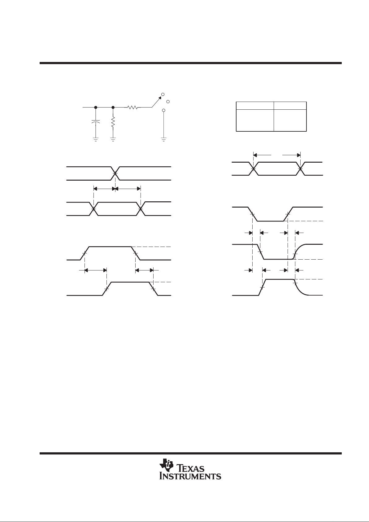
PARAMETER MEASUREMENT INFORMATION
V
CC
= 1.8 V ± 0.15 V
VCC/2
VCC/2
VCC/2VCC/2
VCC/2VCC/2
VCC/2VCC/2
V
OH
V
OL
t
h
t
su
From Output
Under Test
CL = 30 pF
(see Note A)
LOAD CIRCUIT
S1
Open
GND
1 kΩ
1 kΩ
Output
Control
(low-level
enabling)
Output
Waveform 1
S1 at 2 × V
CC
(see Note B)
Output
Waveform 2
S1 at GND
(see Note B)
t
PZL
t
PZH
t
PLZ
t
PHZ
0 V
VOL + 0.15 V
VOH – 0.15 V
0 V
V
CC
0 V
0 V
t
w
V
CC
V
CC
VOLTAGE WAVEFORMS
SETUP AND HOLD TIMES
VOLTAGE WAVEFORMS
PULSE DURATION
VOLTAGE WAVEFORMS
ENABLE AND DISABLE TIMES
Timing
Input
Data
Input
Input
t
pd
t
PLZ/tPZL
t
PHZ/tPZH
Open
2 × V
CC
GND
TEST S1
NOTES: A. CL includes probe and jig capacitance.
B. Waveform 1 is for an output with internal conditions such that the output is low except when disabled by the output control.
Waveform 2 is for an output with internal conditions such that the output is high except when disabled by the output control.
C. All input pulses are supplied by generators having the following characteristics: PRR ≤ 10 MHz, ZO = 50 Ω, tr≤ 2 ns, tf ≤ 2 ns.
D. The outputs are measured one at a time with one transition per measurement.
E. t
PLZ
and t
PHZ
are the same as t
dis
.
F. t
PZL
and t
PZH
are the same as ten.
G. t
PLH
and t
PHL
are the same as tpd.
0 V
V
CC
VCC/2
t
PHL
VCC/2 VCC/2
V
CC
0 V
V
OH
V
OL
Input
Output
VOLTAGE WAVEFORMS
PROPAGATION DELAY TIMES
VCC/2 VCC/2
t
PLH
2 × V
CC
V
CC
Figure 1. Load Circuit and Voltage Waveforms
Page 7
SN74ALVCH32374
32-BIT EDGE-TRIGGERED D-TYPE FLIP-FLOP
WITH 3-STATE OUTPUTS
SCES283 – OCTOBER 1999
7
POST OFFICE BOX 655303 • DALLAS, TEXAS 75265
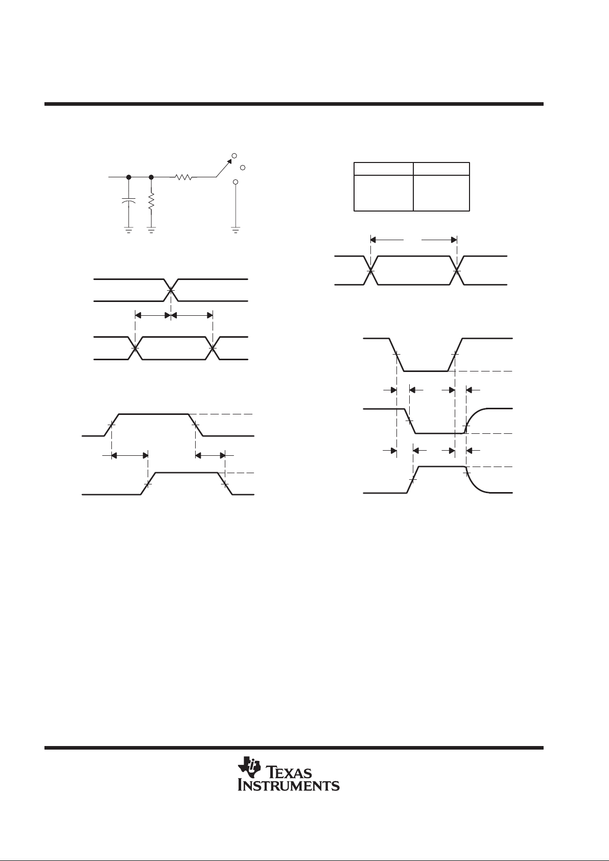
PARAMETER MEASUREMENT INFORMATION
V
CC
= 2.5 V ± 0.2 V
VCC/2
VCC/2
VCC/2VCC/2
VCC/2VCC/2
VCC/2VCC/2
V
OH
V
OL
t
h
t
su
From Output
Under Test
CL = 30 pF
(see Note A)
LOAD CIRCUIT
S1
Open
GND
500 Ω
500 Ω
Output
Control
(low-level
enabling)
Output
Waveform 1
S1 at 2 × V
CC
(see Note B)
Output
Waveform 2
S1 at GND
(see Note B)
t
PZL
t
PZH
t
PLZ
t
PHZ
0 V
VOL + 0.15 V
VOH – 0.15 V
0 V
V
CC
0 V
0 V
t
w
V
CC
V
CC
VOLTAGE WAVEFORMS
SETUP AND HOLD TIMES
VOLTAGE WAVEFORMS
PULSE DURATION
VOLTAGE WAVEFORMS
ENABLE AND DISABLE TIMES
Timing
Input
Data
Input
Input
t
pd
t
PLZ/tPZL
t
PHZ/tPZH
Open
2 × V
CC
GND
TEST S1
NOTES: A. CL includes probe and jig capacitance.
B. Waveform 1 is for an output with internal conditions such that the output is low except when disabled by the output control.
Waveform 2 is for an output with internal conditions such that the output is high except when disabled by the output control.
C. All input pulses are supplied by generators having the following characteristics: PRR ≤ 10 MHz, ZO = 50 Ω, tr≤ 2 ns, tf≤ 2 ns.
D. The outputs are measured one at a time with one transition per measurement.
E. t
PLZ
and t
PHZ
are the same as t
dis
.
F. t
PZL
and t
PZH
are the same as ten.
G. t
PLH
and t
PHL
are the same as tpd.
0 V
V
CC
VCC/2
t
PHL
VCC/2 VCC/2
V
CC
0 V
V
OH
V
OL
Input
Output
VOLTAGE WAVEFORMS
PROPAGATION DELAY TIMES
VCC/2 VCC/2
t
PLH
2 × V
CC
V
CC
Figure 2. Load Circuit and Voltage Waveforms
Page 8
SN74ALVCH32374
32-BIT EDGE-TRIGGERED D-TYPE FLIP-FLOP
WITH 3-STATE OUTPUTS
SCES283 – OCTOBER 1999
8
POST OFFICE BOX 655303 • DALLAS, TEXAS 75265
PARAMETER MEASUREMENT INFORMATION
V
CC
= 2.7 V AND 3.3 V ± 0.3 V
t
PZL
t
PZH
V
OH
V
OL
t
h
t
su
From Output
Under Test
CL = 50 pF
(see Note A)
LOAD CIRCUIT
S1
6 V
Open
GND
500 Ω
500 Ω
t
PLH
t
PHL
Output
Control
(low-level
enabling)
Output
Waveform 1
S1 at 6 V
(see Note B)
Output
Waveform 2
S1 at GND
(see Note B)
t
PLZ
t
PHZ
2.7 V
0 V
V
OH
V
OL
0 V
VOL + 0.3 V
VOH – 0.3 V
0 V
2.7 V
0 V
0 V
2.7 V
0 V
t
w
Input
2.7 V
2.7 V
3 V
VOLTAGE WAVEFORMS
SETUP AND HOLD TIMES
VOLTAGE WAVEFORMS
PROPAGATION DELAY TIMES
VOLTAGE WAVEFORMS
PULSE DURATION
VOLTAGE WAVEFORMS
ENABLE AND DISABLE TIMES
Timing
Input
Data
Input
Output
Input
t
pd
t
PLZ/tPZL
t
PHZ/tPZH
Open
6 V
GND
TEST S1
NOTES: A. CL includes probe and jig capacitance.
B. Waveform 1 is for an output with internal conditions such that the output is low except when disabled by the output control.
Waveform 2 is for an output with internal conditions such that the output is high except when disabled by the output control.
C. All input pulses are supplied by generators having the following characteristics: PRR ≤ 10 MHz, ZO = 50 Ω, tr ≤2.5 ns, tf ≤2.5 ns.
D. The outputs are measured one at a time with one transition per measurement.
E. t
PLZ
and t
PHZ
are the same as t
dis
.
F. t
PZL
and t
PZH
are the same as ten.
G. t
PLH
and t
PHL
are the same as tpd.
1.5 V
1.5 V 1.5 V
1.5 V 1.5 V
1.5 V 1.5 V
1.5 V
1.5 V
1.5 V 1.5 V
1.5 V 1.5 V
Figure 3. Load Circuit and Voltage Waveforms
Page 9

IMPORTANT NOTICE
T exas Instruments and its subsidiaries (TI) reserve the right to make changes to their products or to discontinue
any product or service without notice, and advise customers to obtain the latest version of relevant information
to verify, before placing orders, that information being relied on is current and complete. All products are sold
subject to the terms and conditions of sale supplied at the time of order acknowledgement, including those
pertaining to warranty, patent infringement, and limitation of liability.
TI warrants performance of its semiconductor products to the specifications applicable at the time of sale in
accordance with TI’s standard warranty. Testing and other quality control techniques are utilized to the extent
TI deems necessary to support this warranty. Specific testing of all parameters of each device is not necessarily
performed, except those mandated by government requirements.
CERT AIN APPLICATIONS USING SEMICONDUCTOR PRODUCTS MAY INVOLVE POTENTIAL RISKS OF
DEATH, PERSONAL INJURY, OR SEVERE PROPERTY OR ENVIRONMENTAL DAMAGE (“CRITICAL
APPLICATIONS”). TI SEMICONDUCTOR PRODUCTS ARE NOT DESIGNED, AUTHORIZED, OR
WARRANTED TO BE SUITABLE FOR USE IN LIFE-SUPPORT DEVICES OR SYSTEMS OR OTHER
CRITICAL APPLICATIONS. INCLUSION OF TI PRODUCTS IN SUCH APPLICA TIONS IS UNDERSTOOD T O
BE FULLY AT THE CUSTOMER’S RISK.
In order to minimize risks associated with the customer’s applications, adequate design and operating
safeguards must be provided by the customer to minimize inherent or procedural hazards.
TI assumes no liability for applications assistance or customer product design. TI does not warrant or represent
that any license, either express or implied, is granted under any patent right, copyright, mask work right, or other
intellectual property right of TI covering or relating to any combination, machine, or process in which such
semiconductor products or services might be or are used. TI’s publication of information regarding any third
party’s products or services does not constitute TI’s approval, warranty or endorsement thereof.
Copyright 1999, Texas Instruments Incorporated
 Loading...