

Page 1
SN54ABT18652, SN74ABT18652
SCAN TEST DEVICES WITH
18-BIT BUS TRANSCEIVERS AND REGISTERS
SCBS132A – AUGUST 1992 – REVISED OCTOBER 1992
• Members of the Texas Instruments
SCOPE
Family of Testability Products
• Members of the Texas Instruments
Widebus
Family
• Compatible With the IEEE Standard
1149.1-1990 (JTAG) Test Access Port and
Boundary-Scan Architecture
• Include D-Type Flip-Flops and Control
Circuitry to Provide Multiplexed
Transmission of Stored and Real-Time Data
• Two Boundary-Scan Cells per I/O for
Greater Flexibility
• State-of-the-Art
Significantly Reduces Power Dissipation
EPIC-ΙΙB
1A3
1A4
1A5
GND
1A6
1A7
1A8
1A9
NC
V
CC
2A1
2A2
2A3
GND
2A4
2A5
2A6
BiCMOS Design
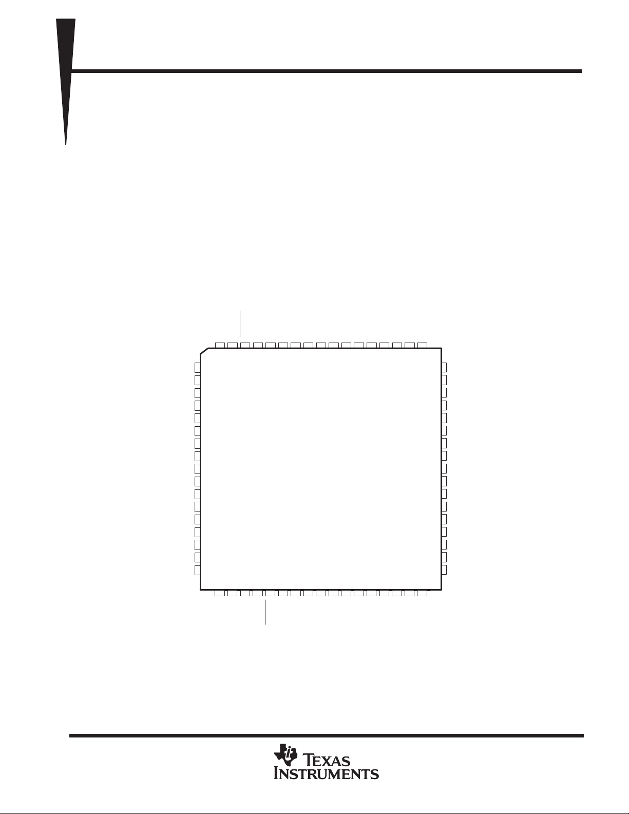
SN54ABT18652 . . . HV PACKAGE
1A2
1A1
1OEBA
GND
67 66 65 64 6368 62 60 59 5861
1
2
3
4
5
6
7
8
9
10
11
12
13
14
15
16
17
19 20
21
22 23 24 25
1SAB
(TOP VIEW)
VNCTMS
1CLKAB
TDO
•
• Packaged in 64-Pin Plastic Shrink Quad Flat
CC
26 27 28 29 30
1SBA
1CLKBA
57 561855 54 53 52
SCOPE
Instruction Set
– IEEE Standard 1149.1-1990 Required
Instructions, Optional INTEST, and
P1149.1A CLAMP and HIGHZ
– Parallel Signature Analysis at Inputs With
Masking Option
– Pseudo-Random Pattern Generation
From Outputs
– Sample Inputs/Toggle Outputs
– Binary Count From Outputs
– Device Identification
– Even-Parity Opcodes
Pack (PM) and 68-Pin Ceramic Quad Flat
Pack (HV)
1OEAB
GND
1B1
1B2
1B3
1B4
51
1B5
50
1B6
49
GND
48
1B7
47
1B8
46
1B9
45
V
44
CC
NC
43
2B1
42
2B2
41
2B3
40
2B4
39
GND
38
2B5
37
2B6
36
2B7
35
31 32 33 34
PRODUCT PREVIEW
2A7
NC – No internal connection
PRODUCT PREVIEW information concerns products in the formative or
design phase of development. Characteristic data and other
specifications are design goals. Texas Instruments reserves the right to
change or discontinue these products without notice.
CC
NC
2A8
2A9
GND
2OEBA
POST OFFICE BOX 655303 • DALLAS, TEXAS 75265
2SAB
2CLKAB
TDI
V
TCK
2CLKBA
GND
2SBA
2B9
2B8
2OEAB
Copyright 1992, Texas Instruments Incorporated
1
Page 2
SN54ABT18652, SN74ABT18652
SCAN TEST DEVICES WITH
18-BIT BUS TRANSCEIVERS AND REGISTERS
SCBS132A – AUGUST 1992 – REVISED OCTOBER 1992
1A3
1A4
1A5
GND
1A6
1A7
1A8
1A9
V
CC
2A1
2A2
PRODUCT PREVIEW
2A3
GND
2A4
2A5
2A6
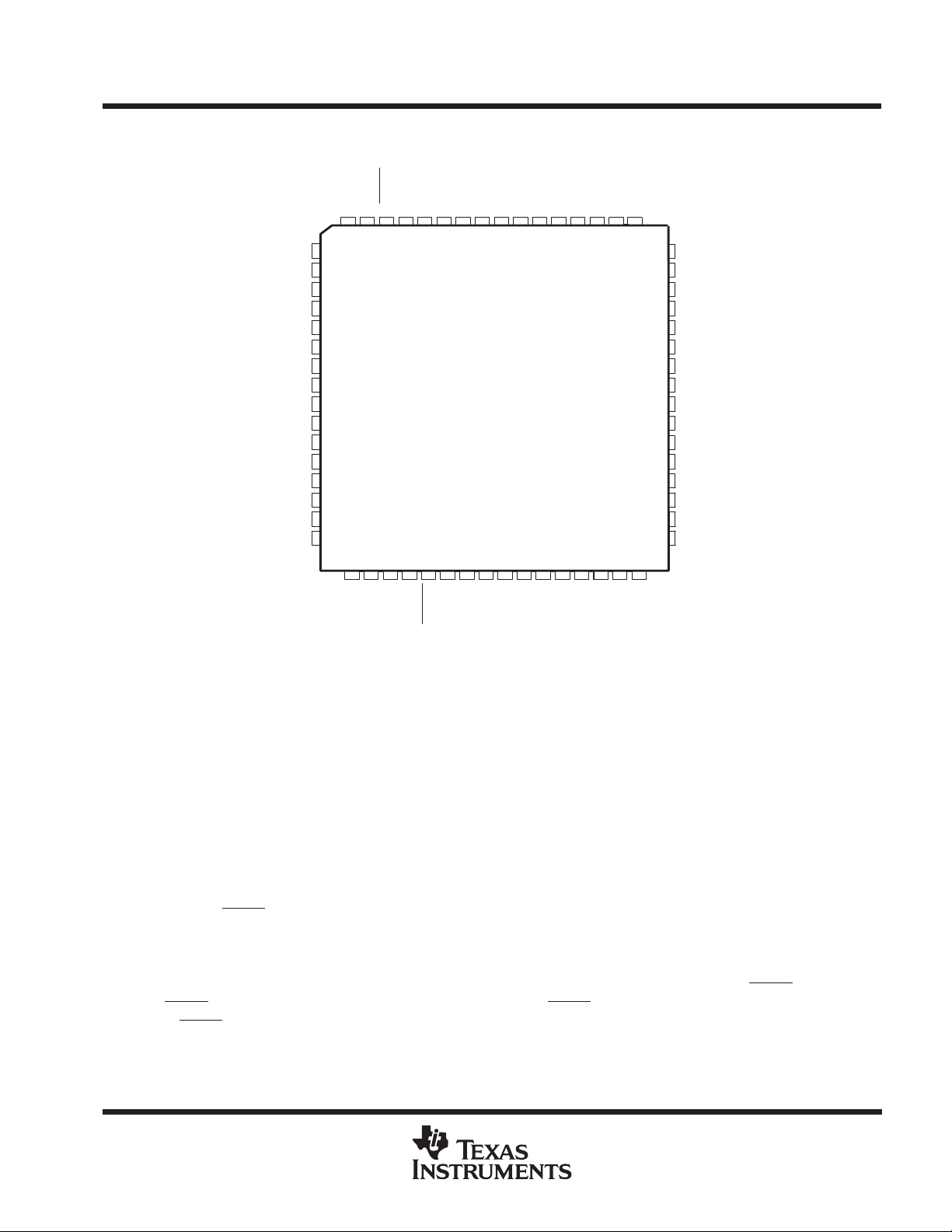
SN74ABT18652 ...PM PACKAGE
1OEBA
1A2
1A1
63 62 61 60 5964 58 56 55 5457
1
2
3
4
5
6
7
8
9
10
11
12
13
14
15
16
18 19
GND
1SAB
21 22 23 24
20
(TOP VIEW)
CC
1CLKAB
TDO
V
1SBA
TMS
25 26 27 28 29
1OEAB
1CLKBA
53 521751 50 49
1B1
GND
30 31 32
1B2
1B3
48
47
46
45
44
43
42
41
40
39
38
37
36
35
34
33
1B4
1B5
1B6
GND
1B7
1B8
1B9
V
CC
2B1
2B2
2B3
2B4
GND
2B5
2B6
2B7
CC
2A7
2A8
2A9
GND
2OEAB
2SAB
2CLKAB
TDI
V
TCK
2CLKBA
GND
2SBA
2B9
2OEAB
2B8
description
The SN54ABT18652 and SN74ABT18652 scan test devices with 18-bit bus transceivers and registers are
members of the T exas Instruments SCOPE testability IC family . This family of devices supports IEEE Standard
1149.1-1990 boundary scan to facilitate testing of complex circuit board assemblies. Scan access to the test
circuitry is accomplished via the 4-wire test access port (TAP) interface.
In the normal mode, these devices are 18-bit bus transceivers and registers that allow for multiplexed
transmission of data directly from the input bus or from the internal registers. They can be used either as two
9-bit transceivers or one 18-bit transceiver. The test circuitry can be activated by the TAP to take snapshot
samples of the data appearing at the device pins or to perform a self test on the boundary test cells. Activating
the TAP in the normal mode does not affect the functional operation of the SCOPE bus transceivers and
registers.
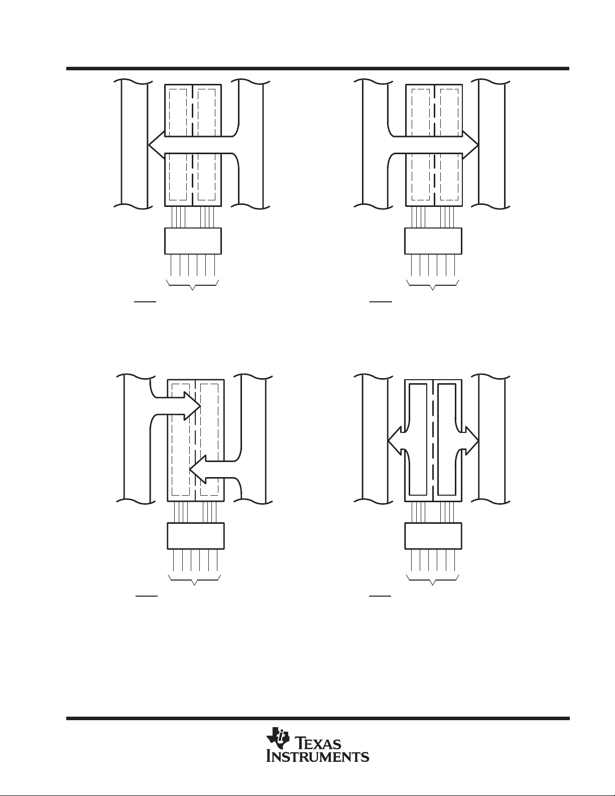
Data flow in each direction is controlled by clock (CLKAB and CLKBA), select (SAB and SBA), and output-enable
(OEAB and OEBA
the low-to-high transition of CLKAB. When SAB is low, real-time A data is selected for presentation to the B bus
(transparent mode). When SAB is high, stored A data is selected for presentation to the B bus (registered mode).
When OEAB is high, the B outputs are active. When OEAB is low, the B outputs are in the high-impedance state.
Control for B-to-A data flow is similar to that for A-to-B data flow but uses CLKBA, SBA, and OEBA
the OEBA input is active-low, the A outputs are active when OEBA is low and are in the high-impedance state
when OEBA
with the ′ABT18652.
) inputs. For A-to-B data flow, data on the A bus is clocked into the associated registers on
inputs. Since
is high. Figure 1 illustrates the four fundamental bus-management functions that can be performed
2
POST OFFICE BOX 655303 • DALLAS, TEXAS 75265
Page 3
SN54ABT18652, SN74ABT18652
OPERATION OR FUNCTION
SCAN TEST DEVICES WITH
18-BIT BUS TRANSCEIVERS AND REGISTERS
SCBS132A – AUGUST 1992 – REVISED OCTOBER 1992
description (continued)
In the test mode, the normal operation of the SCOPE bus transceivers and registers is inhibited, and the test
circuitry is enabled to observe and control the I/O boundary of the device. When enabled, the test circuitry can
perform boundary scan test operations according to the protocol described in IEEE Standard 1149.1-1990.
Four dedicated test pins are used to observe and control the operation of the test circuitry: test data input (TDI),
test data output (TDO), test mode select (TMS), and test clock (TCK). Additionally , the test circuitry can perform
other testing functions such as parallel signature analysis on data inputs and pseudo-random pattern generation
from data outputs. All testing and scan operations are synchronized to the TAP interface.
Additional flexibility is provided in the test mode through the use of two boundary scan cells (BSCs) for each
I/O pin. This allows independent test data to be captured and forced at either bus (A or B). A PSA/COUNT
instruction is also included to ease the testing of memories and other circuits where a binary count addressing
scheme is useful.
The SN54ABT18652 is characterized over the full military temperature range of –55°C to 125°C. The
SN74ABT18652 is characterized for operation from –40°C to 85°C.
FUNCTION TABLE
(normal mode, each 9-bit section)
INPUTS
OEAB OEBA CLKAB CLKBA SAB SBA A1 THRU A9 B1 THRU B9
L H L L X X Input disabled Input disabled Isolation
L H ↑↑X X Input Input Store A and B data
X H ↑ L X X Input Unspecified
H H ↑↑X
L XL ↑ X X Unspecified
L L ↑↑XX‡Output Input Store B in both registers
L L X X X L Output Input Real-time B data to A bus
L L X L X H Output Input Stored B data to A bus
H H X X L X Input Output Real-time A data to B bus
H H L X H X Input Output Stored A data to B bus
H L L L H H Output Output
†
The data output functions can be enabled or disabled by a variety of level combinations at the OEAB or OEBA
always enabled; i.e., data at the bus pins is stored on every low-to-high transition on the clock inputs.
‡
Select control = L: clocks can occur simultaneously.
Select control = H: clocks must be staggered in order to load both registers.
‡
X Input Output Store A in both registers
DATA I/O
†
†
Input Hold A, store B
Store A, hold B
Stored A data to B bus and
stored B data to A bus
inputs. Data input functions are
PRODUCT PREVIEW
POST OFFICE BOX 655303 • DALLAS, TEXAS 75265
3
Page 4
SN54ABT18652, SN74ABT18652
SCAN TEST DEVICES WITH
18-BIT BUS TRANSCEIVERS AND REGISTERS
SCBS132A – AUGUST 1992 – REVISED OCTOBER 1992
BUS A
PRODUCT PREVIEW
OEAB
OEBA
LL
CLKABXCLKBAXSABXSBA
REAL-TIME TRANSFER
BUS B TO BUS A
BUS B
L
BUS A
OEAB OEBA
HH
BUS B
CLKABXCLKBAXSABLSBA
X
REAL-TIME TRANSFER
BUS A TO BUS B
OEAB
X
L
L
BUS A
CLKAB CLKBAXSABXSBA
OEBA
H
X
H
↑
XX
STORAGE FROM
A, B, OR A AND B
↑
↑↑
BUS B
OEAB OEBA
X
X
X
X
HL L HH
BUS A
TRANSFER STORED DA TA
Figure 1. Bus-Management Functions
BUS B
CLKAB CLKBA SAB SBA
L
TO A AND/OR B
4
POST OFFICE BOX 655303 • DALLAS, TEXAS 75265
Page 5

functional block diagram
SN54ABT18652, SN74ABT18652
SCAN TEST DEVICES WITH
18-BIT BUS TRANSCEIVERS AND REGISTERS
SCBS132A – AUGUST 1992 – REVISED OCTOBER 1992
1OEAB
1OEBA
1CLKBA
1SBA
1CLKAB
1SAB
1A1
2OEAB
2OEBA
2CLKBA
2SBA
2CLKAB
2SAB
63
30
21
27
28
23
22
53
62
55
54
59
60
Boundary-Scan Register
C1
1D
1 of 9 Channels
C1
1D
51
1B1
10
2A1
V
CC
24
TDI
V
CC
56
TMS
26
TCK
Pin numbers shown are for the PM package.
C1
1D
Bypass Register
Boundary-Control
Register
Identification
Register
Instruction
Register
TAP
Controller
1 of 9 Channels
C1
1D
58
40
2B1
PRODUCT PREVIEW
TDO
POST OFFICE BOX 655303 • DALLAS, TEXAS 75265
5
Page 6

SN54ABT18652, SN74ABT18652
UNIT
SCAN TEST DEVICES WITH
18-BIT BUS TRANSCEIVERS AND REGISTERS
SCBS132A – AUGUST 1992 – REVISED OCTOBER 1992
absolute maximum ratings over operating free-air temperature range (unless otherwise noted)
Supply voltage range, V
Input voltage range, VI: except I/O ports (see Note 1) –0.5 V to 7 V. . . . . . . . . . . . . . . . . . . . . . . . . . . . . . . . . .
Voltage range applied to any output in the high state or power-off state, VO –0.5 V to 5.5 V. . . . . . . . . . . . .
Current into any output in the low state, IO: SN54ABT18652 96 mA. . . . . . . . . . . . . . . . . . . . . . . . . . . . . . . . . .
Input clamp current, I
Output clamp current, I
Maximum power dissipation at TA = 55°C (in still air) (see Note 2) 885 mW. . . . . . . . . . . . . . . . . . . . . . . . . . . .
Storage temperature range –65°C to 150°C. . . . . . . . . . . . . . . . . . . . . . . . . . . . . . . . . . . . . . . . . . . . . . . . . . . . . . .
†
Stresses beyond those listed under “absolute maximum ratings” may cause permanent damage to the device. These are stress ratings only, and
functional operation of the device at these or any other conditions beyond those indicated under “recommended operating conditions” is not
implied. Exposure to absolute-maximum-rated conditions for extended periods may affect device reliability.
NOTES: 1. The input and output negative-voltage ratings may be exceeded if the input and output clamp-current ratings are observed.
2. For the SN74ABT18652 (PM package), the power derating factor for ambient temperatures greater than 55°C is –10.5 mW/°C.
–0.5 V to 7 V. . . . . . . . . . . . . . . . . . . . . . . . . . . . . . . . . . . . . . . . . . . . . . . . . . . . . . . . . .
CC
I/O ports (see Note 1) –0.5 V to 5.5 V. . . . . . . . . . . . . . . . . . . . . . . . . . . . . . . . . . . . . . .
SN74ABT18652 128 mA. . . . . . . . . . . . . . . . . . . . . . . . . . . . . . . . . .
(V
< 0) –18 mA. . . . . . . . . . . . . . . . . . . . . . . . . . . . . . . . . . . . . . . . . . . . . . . . . . . . . . . . . . .
IK
I
(V
< 0) –50 mA. . . . . . . . . . . . . . . . . . . . . . . . . . . . . . . . . . . . . . . . . . . . . . . . . . . . . . .
OK
O
recommended operating conditions (see Note 3)
PRODUCT PREVIEW
V
CC
V
IH
V
IL
V
I
I
OH
I
OL
∆t/∆v Input transition rise or fall rate 10 10 ns/V
T
A
NOTE 3: Unused or floating pins (input or I/O) must be held high or low.
Supply voltage 4.5 5.5 4.5 5.5 V
High-level input voltage 2 2 V
Low-level input voltage 0.8 0.8 V
Input voltage 0 V
High-level output current –24 –32 mA
Low-level output current 48 64 mA
Operating free-air temperature –55 125 –40 85 °C
SN54ABT18652 SN74ABT18652
MIN MAX MIN MAX
CC
0 V
CC
†
V
6
POST OFFICE BOX 655303 • DALLAS, TEXAS 75265
Page 7

SN54ABT18652, SN74ABT18652
PARAMETER
TEST CONDITIONS
UNIT
V
V
V
4.5 V
V
V
V
V
µ
I
V
V
GND
µ
,
V
CC
5.5 V,
A or B orts
SCAN TEST DEVICES WITH
18-BIT BUS TRANSCEIVERS AND REGISTERS
SCBS132A – AUGUST 1992 – REVISED OCTOBER 1992
electrical characteristics over recommended operating free-air temperature range (unless
otherwise noted) (see Note 4)
TA = 25°C SN54ABT18652 SN74ABT18652
MIN TYP†MAX MIN MAX MIN MAX
V
IK
OH
OL
I
I
IH
I
IL
I
OZH
I
OZL
I
off
I
CEX
§
I
O
I
CC
∆I
CC
C
i
C
io
C
o
NOTE 4: Preliminary specifications based on SPICE analysis
* On products compliant to MIL-STD-883, Class B, this parameter does not apply.
†
All typical values are at VCC = 5 V.
‡
The parameters I
§
Not more than one output should be tested at a time, and the duration of the test should not exceed one second.
¶
This is the increase in supply current for each input that is at the specified TTL voltage level rather than VCC or GND.
VCC = 4.5 V, II = –18 mA –1.2 –1.2 –1.2 V
VCC = 4.5 V, IOH = – 3 mA 2.5 2.5 2.5
VCC = 5 V, IOH = – 3 mA 3 3 3
=
CC
= 4.5
CC
VCC = 5.5 V,
=
I
CC
VCC = 5.5 V, VI = V
VCC = 5.5 V, VI = GND TDI, TMS –160 –160 –160 µA
‡
VCC = 5.5 V, VO = 2.7 V 50 50 50 µA
‡
VCC = 5.5 V, VO = 0.5 V –50 –50 –50 µA
VCC = 0, VI or VO ≤ 5.5 V ±100 ±450 ±100 µA
VCC = 5.5 V, VO = 5.5 V Outputs high 50 50 50 µA
VCC = 5.5 V, VO = 2.5 V –50 –100 –180 –50 –180 –50 –180 mA
V
= 5.5 V
IO = 0,
VI = VCC or
GND
VCC = 5.5 V, One input at 3.4 V,
¶
Other inputs at VCC or GND
VI = 2.5 V or 0.5 V Control inputs 4 pF
VO = 2.5 V or 0.5 V A or B ports 10 pF
VO = 2.5 V or 0.5 V TDO 8 pF
and I
OZH
IOH = – 24 mA 2 2
IOH = – 32 mA 2* 2
IOL = 48 mA 0.55 0.55
IOL = 64 mA 0.55* 0.55
CLK, OEAB,
or
CC
include the input leakage current.
OZL
OEBA
A or B ports ±100 ±100 ±100
TDI, TMS 10 10 10 µA
Outputs high 4 4 4
Outputs low 80 80 80 mA
p
Outputs
disabled
, S, TCK
±1 ±1 ±1
4 4 4
1.5 1.5 1.5 mA
A
PRODUCT PREVIEW
POST OFFICE BOX 655303 • DALLAS, TEXAS 75265
7
Page 8

SN54ABT18652, SN74ABT18652
UNIT
UNIT
SCAN TEST DEVICES WITH
18-BIT BUS TRANSCEIVERS AND REGISTERS
SCBS132A – AUGUST 1992 – REVISED OCTOBER 1992
timing requirements over recommended ranges of supply voltage and operating free-air
temperature (unless otherwise noted) (normal mode) (see Note 4 and Figure 2)
SN54ABT18652 SN74ABT18652
MIN MAX MIN MAX
f
clock
t
w
t
su
t
h
timing requirements over recommended ranges of supply voltage and operating free-air
temperature (unless otherwise noted) (test mode) (see Note 4 and Figure 2)123
f
clock
t
w
PRODUCT PREVIEW
t
su
t
h
t
d
t
r
NOTE 4: Preliminary specifications based on SPICE analysis
Clock frequency CLKAB or CLKBA 0 100 0 100 MHz
Pulse duration CLKAB or CLKBA high or low 3 ns
Setup time A before CLKAB↑ or B before CLKBA↑ 5 ns
Hold time A after CLKAB↑ or B after CLKBA↑ 0 ns
SN54ABT18652 SN74ABT18652
MIN MAX MIN MAX
Clock frequency TCK 0 50 0 50 MHz
Pulse duration TCK high or low 5 ns
A, B, CLK, OEAB, OEBA, or S before TCK↑ 5
Setup time
Hold time
Delay time Power up to TCK↑ 50 ns
Rise time VCC power up 1 µs
TDI before TCK↑
TMS before TCK↑ 6
A, B, CLK, OEAB, OEBA, or S after TCK↑ 0
TDI after TCK↑
TMS after TCK↑ 0
6
0
ns
ns
8
POST OFFICE BOX 655303 • DALLAS, TEXAS 75265
Page 9

SN54ABT18652, SN74ABT18652
(INPUT)
(OUTPUT)
A or B
B or A
ns
CLKAB or CLKBA
B or A
ns
SAB or SBA
B or A
ns
OEAB
OEBA
B or A
ns
OEAB
OEBA
B or A
ns
(INPUT)
(OUTPUT)
TCK↓
A or B
ns
TCK↓
TDO
ns
TCK↓
A or B
ns
TCK↓
TDO
ns
TCK↓
A or B
ns
TCK↓
TDO
ns
SCAN TEST DEVICES WITH
18-BIT BUS TRANSCEIVERS AND REGISTERS
SCBS132A – AUGUST 1992 – REVISED OCTOBER 1992
switching characteristics over recommended ranges of supply voltage and operating free-air
temperature (unless otherwise noted) (normal mode) (see Note 4 and Figure 2)
VCC = 5 V,
TA = 25°C
MIN TYP MAX MIN MAX MIN MAX
PARAMETER
f
max
t
PLH
t
PHL
t
PLH
t
PHL
t
PLH
t
PHL
t
PZH
t
PZL
t
PHZ
t
PLZ
FROM
CLKAB or CLKBA 100 130 100 100 MHz
or
or
TO
switching characteristics over recommended ranges of supply voltage and operating free-air
temperature (unless otherwise noted) (test mode) (see Note 4 and Figure 2)123
PARAMETER
f
max
t
PLH
t
PHL
t
PLH
t
PHL
t
PZH
t
PZL
t
PZH
t
PZL
t
PHZ
t
PLZ
t
PHZ
t
PLZ
NOTE 4: Preliminary specifications based on SPICE analysis
FROM
TCK 50 90 50 50 MHz
TO
VCC = 5 V,
TA = 25°C
MIN TYP MAX MIN MAX MIN MAX
SN54ABT18652 SN74ABT18652
1 6
1 6
2 6
2 6
2 8
2 8
2 7.5
2 7.5
2 7.5
2 7.5
SN54ABT18652 SN74ABT18652
3 12
3 12
2 7
2 7
3 14
3 14
2 8
2 8
3 14
3 14
2 8
2 8
UNIT
UNIT
PRODUCT PREVIEW
POST OFFICE BOX 655303 • DALLAS, TEXAS 75265
9
Page 10

SN54ABT18652, SN74ABT18652
SCAN TEST DEVICES WITH
18-BIT BUS TRANSCEIVERS AND REGISTERS
SCBS132A – AUGUST 1992 – REVISED OCTOBER 1992
PARAMETER MEASUREMENT INFORMATION
From Output
Under Test
CL = 50 pF
(see Note A)
Input
500 Ω
500 Ω
LOAD CIRCUIT FOR OUTPUTS
t
w
1.5 V 1.5 V
S1
PRODUCT PREVIEW
VOLTAGE WAVEFORMS
PULSE DURATION
7 V
Open
GND
3 V
0 V
Timing Input
Data Input
TEST S1
t
PLH/tPHL
t
PLZ/tPZL
t
PHZ/tPZH
t
su
1.5 V 1.5 V
VOLTAGE WAVEFORMS
SETUP AND HOLD TIMES
Open
Open
1.5 V
t
7 V
h
3 V
0 V
3 V
0 V
Input
(see Note B)
t
PLH
Output
t
PHL
Output
PROPAGATION DELAY TIMES
INVERTING AND NON-INVERTING OUTPUTS
NOTES: A. CL includes probe and jig capacitance.
B. All input pulses are supplied by generators having the following characteristics: PRR ≤ 10 MHz, ZO = 50 Ω, tr ≤ 2.5 ns, tf≤ 2.5 ns.
C. Waveform 1 is for an output with internal conditions such that the output is low except when disabled by the output control.
Waveform 2 is for an output with internal conditions such that the output is high except when disabled by the output control.
D. The outputs are measured one at a time with one transition per measurement.
1.5 V 1.5 V
1.5 V
VOLTAGE WAVEFORMS
Figure 2. Load Circuit and Voltage Waveforms
t
PHL
1.5 V
t
PLH
1.5 V1.5 V
3 V
0 V
V
V
V
V
OH
OL
OH
OL
Output
Control
Output
Waveform 1
S1 at 7 V
(see Note C)
Output
Waveform 2
S1 at Open
(see Note C)
1.5 V
t
PZL
t
PLZ
1.5 V
t
t
PZH
ENABLE AND DISABLE TIMES
LOW- AND HIGH-LEVEL ENABLING
PHZ
1.5 V
VOLTAGE WAVEFORMS
1.5 V
VOL + 0.3 V
VOH – 0.3 V
3 V
0 V
3.5 V
V
OL
V
OH
[
0 V
10
POST OFFICE BOX 655303 • DALLAS, TEXAS 75265
Page 11

IMPORTANT NOTICE
T exas Instruments and its subsidiaries (TI) reserve the right to make changes to their products or to discontinue
any product or service without notice, and advise customers to obtain the latest version of relevant information
to verify, before placing orders, that information being relied on is current and complete. All products are sold
subject to the terms and conditions of sale supplied at the time of order acknowledgement, including those
pertaining to warranty, patent infringement, and limitation of liability.
TI warrants performance of its semiconductor products to the specifications applicable at the time of sale in
accordance with TI’s standard warranty. Testing and other quality control techniques are utilized to the extent
TI deems necessary to support this warranty . Specific testing of all parameters of each device is not necessarily
performed, except those mandated by government requirements.
CERTAIN APPLICA TIONS USING SEMICONDUCTOR PRODUCTS MA Y INVOLVE POTENTIAL RISKS OF
DEATH, PERSONAL INJURY, OR SEVERE PROPERTY OR ENVIRONMENTAL DAMAGE (“CRITICAL
APPLICATIONS”). TI SEMICONDUCTOR PRODUCTS ARE NOT DESIGNED, AUTHORIZED, OR
WARRANTED TO BE SUITABLE FOR USE IN LIFE-SUPPORT DEVICES OR SYSTEMS OR OTHER
CRITICAL APPLICA TIONS. INCLUSION OF TI PRODUCTS IN SUCH APPLICATIONS IS UNDERST OOD TO
BE FULLY AT THE CUSTOMER’S RISK.
In order to minimize risks associated with the customer’s applications, adequate design and operating
safeguards must be provided by the customer to minimize inherent or procedural hazards.
TI assumes no liability for applications assistance or customer product design. TI does not warrant or represent
that any license, either express or implied, is granted under any patent right, copyright, mask work right, or other
intellectual property right of TI covering or relating to any combination, machine, or process in which such
semiconductor products or services might be or are used. TI’s publication of information regarding any third
party’s products or services does not constitute TI’s approval, warranty or endorsement thereof.
Copyright 1998, Texas Instruments Incorporated
 Loading...