

Datasheet SN54AS286J, SN74AS286N, SN74AS286D, SN74AS286DR, SNJ54AS286FK Datasheet (Texas Instruments)
...Page 1
SN54AS286, SN74AS286
9-BIT PARITY GENERATORS/CHECKERS
WITH BUS-DRIVER PARITY I/O PORT
SDAS050B – DECEMBER 1983 – REVISED DECEMBER 1994
Copyright 1994, Texas Instruments Incorporated
1
POST OFFICE BOX 655303 • DALLAS, TEXAS 75265
• Generate Either Odd or Even Parity for
Nine Data Lines
• Cascadable for n-Bit Parity
• Direct Bus Connection for Parity
Generation or Checking by Using the
Parity I/O Port
• Glitch-Free Bus During Power Up/Down
• Package Options Include Plastic
Small-Outline (D) Packages, Ceramic Chip
Carriers (FK), and Standard Plastic (N) and
Ceramic (J) 300-mil DIPs
description
The SN54AS286 and SN74AS286 universal 9-bit
parity generators/checkers feature a local output
for parity checking and a 48-mA bus-driving
parity input/output (I/O) port for parity
generation/checking. The word-length capability
is easily expanded by cascading.
The transmit (XMIT
) control input is implemented
specifically to accommodate cascading. When
XMIT
is low, the parity tree is disabled and
PARITY ERROR remains at a high logic level
regardless of the input levels. When XMIT
is high,
the parity tree is enabled. PARITY ERROR
indicates a parity error when either an even
number of inputs (A–I) are high and PARITY I/O
is forced to a low logic level, or when an odd
number of inputs are high and PARITY I/O is
forced to a high logic level.
The I/O control circuitry was designed so that the I/O port remains in the high-impedance state during power up
or power down to prevent bus glitches.
The SN54AS286 is characterized for operation over the full military temperature range of –55°C to 125°C. The
SN74AS286 is characterized for operation from 0°C to 70°C.
FUNCTION TABLE
NUMBER OF INPUTS
(A–I) THAT
ARE HIGH
XMIT
PARITY
I/O
PARITY
ERROR
0, 2, 4, 6, 8 l H H
1, 3, 5, 7, 9 l L H
h h H
0, 2, 4, 6, 8
h l L
h h L
1, 3, 5, 7, 9
h l H
h = high input level l = low input level
H = high output level L = low output level
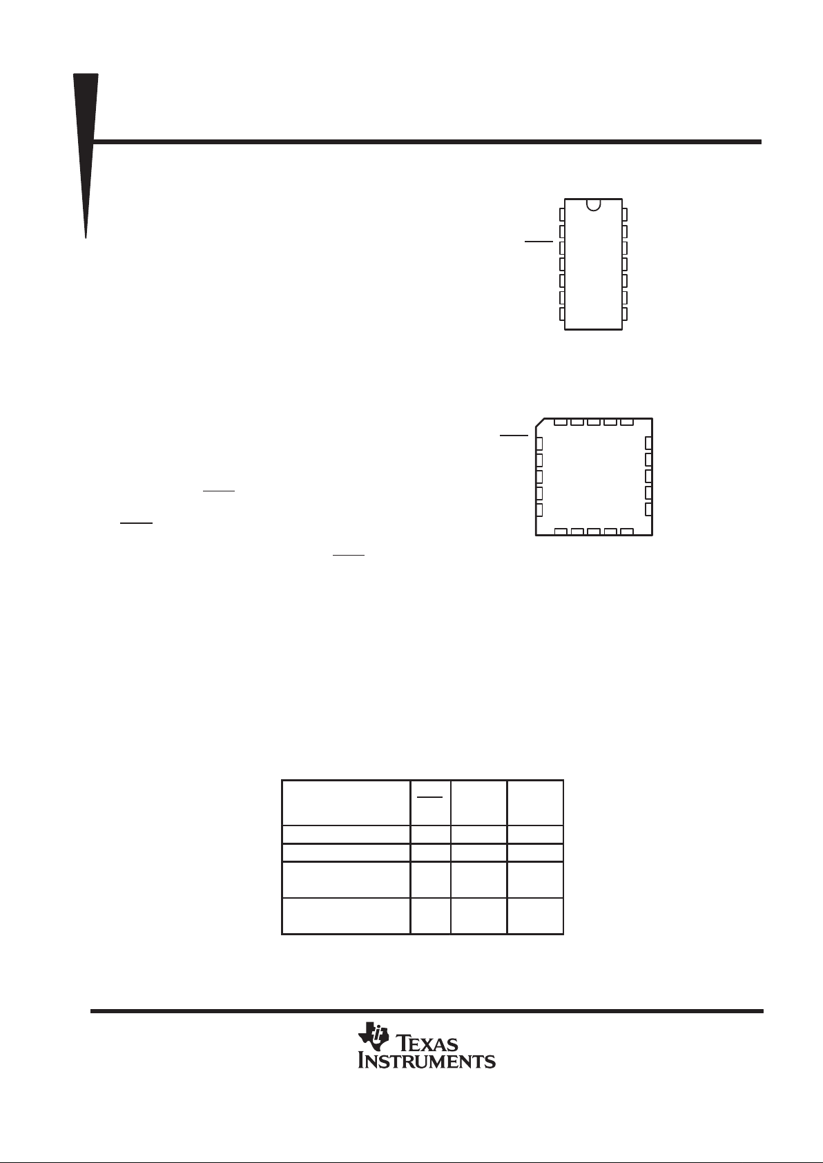
SN54AS286 ...J PACKAGE
SN74AS286 ...D OR N PACKAGE
(TOP VIEW)
SN54AS286 . . . FK PACKAGE
(TOP VIEW)
3212019
910111213
4
5
6
7
8
18
17
16
15
14
E
NC
D
NC
C
XMIT
NC
I
NC
PARITY ERROR
HGNC
A
B
V
F
PARITY I/O
GND
NC
CC
NC – No internal connection
1
2
3
4
5
6
7
14
13
12
11
10
9
8
G
H
XMIT
I
PARITY ERROR
PARITY I/O
GND
V
CC
F
E
D
C
B
A
PRODUCTION DATA information is current as of publication date.
Products conform to specifications per the terms of Texas Instruments
standard warranty. Production processing does not necessarily include
testing of all parameters.
Page 2
SN54AS286, SN74AS286
9-BIT PARITY GENERATORS/CHECKERS
WITH BUS-DRIVER PARITY I/O PORT
SDAS050B – DECEMBER 1983 – REVISED DECEMBER 1994
2
POST OFFICE BOX 655303 • DALLAS, TEXAS 75265
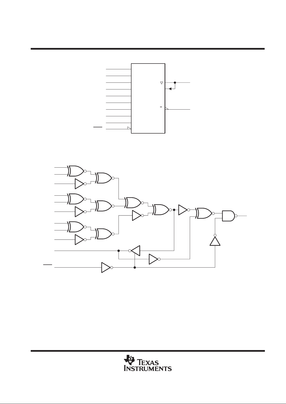
logic symbol
†
2k
8
A
13
F
1
G
2
H
4
I
9
B
10
C
11
D
12
E
EN1
3
PARITY I/O
6
N2
PARITY ERROR
5
XMIT
2, 1
1
†
This symbol is in accordance with ANSI/IEEE Std 91-1984 and IEC Publication 617-12.
Pin numbers shown are for the D, J, and N packages.
logic diagram (positive logic)
PARITY
ERROR
5
8
9
10
11
12
13
1
2
4
6
3
A
B
C
D
E
F
G
H
I
PARITY I/O
XMIT
Pin numbers shown are for the D, J, and N packages.
Page 3
SN54AS286, SN74AS286
9-BIT PARITY GENERATORS/CHECKERS
WITH BUS-DRIVER PARITY I/O PORT
SDAS050B – DECEMBER 1983 – REVISED DECEMBER 1994
3
POST OFFICE BOX 655303 • DALLAS, TEXAS 75265
absolute maximum ratings over operating free-air temperature range (unless otherwise noted)
†
Supply voltage, V
CC
7 V. . . . . . . . . . . . . . . . . . . . . . . . . . . . . . . . . . . . . . . . . . . . . . . . . . . . . . . . . . . . . . . . . . . . . . . .
Input voltage, V
I
7 V. . . . . . . . . . . . . . . . . . . . . . . . . . . . . . . . . . . . . . . . . . . . . . . . . . . . . . . . . . . . . . . . . . . . . . . . . . . .
Voltage applied to a disabled 3-state output 5.5 V. . . . . . . . . . . . . . . . . . . . . . . . . . . . . . . . . . . . . . . . . . . . . . . . . .
Operating free-air temperature range, T
A
: SN54AS286 –55°C to 125°C. . . . . . . . . . . . . . . . . . . . . . . . . . . . . .
SN74AS286 0°C to 70°C. . . . . . . . . . . . . . . . . . . . . . . . . . . . . . . . . .
Storage temperature range –65°C to 150°C. . . . . . . . . . . . . . . . . . . . . . . . . . . . . . . . . . . . . . . . . . . . . . . . . . . . . . .
†
Stresses beyond those listed under “absolute maximum ratings” may cause permanent damage to the device. These are stress ratings only, and
functional operation of the device at these or any other conditions beyond those indicated under “recommended operating conditions” is not
implied. Exposure to absolute-maximum-rated conditions for extended periods may affect device reliability.
recommended operating conditions
SN54AS286 SN74AS286
MIN NOM MAX MIN NOM MAX
UNIT
V
CC
Supply voltage 4.5 5 5.5 4.5 5 5.5 V
V
IH
High-level input voltage 2 2 V
V
IL
Low-level input voltage 0.8 0.8 V
p
PARITY ERROR –2 –2
IOHHigh-level output current
PARITY I/O –12 –15
mA
p
PARITY ERROR 20 20
IOLLow-level output current
PARITY I/O 32 48
mA
T
A
Operating free-air temperature –55 125 0 70 °C
electrical characteristics over recommended operating free-air temperature range (unless
otherwise noted)
SN54AS286 SN74AS286
PARAMETER
TEST CONDITIONS
MIN TYP‡MAX MIN TYP‡MAX
UNIT
V
IK
VCC = 4.5 V, II = –18 mA –1.2 –1.2 V
All outputs VCC = 4.5 V to 5.5 V, IOH = –2 mA VCC –2 VCC –2
IOH = –3 mA 2.4 2.9 2.4 3
V
OH
PARITY I/O VCC = 4.5 V
IOH = –12 mA 2.4
V
IOH = –15 mA 2.4
PARITY ERROR IOL = 20 mA 0.35 0.5 0.35 0.5
V
OL
VCC = 4.5 V
IOL = 32 mA 0.5
V
PARITY I/O
IOL = 48 mA 0.5
PARITY I/O
VI = 5.5 V 0.1 0.1
I
I
All other inputs
V
CC
= 5.5
V
VI = 7 V 0.1 0.1
mA
PARITY I/O
§
50 50
I
IH
All other inputs
V
CC
=
5.5 V
,
V
I
=
2.7 V
20 20
µ
A
PARITY I/O
§
–0.5 –0.5
I
IL
All other inputs
V
CC
= 5.5 V,
V
I
= 0.4
V
–0.5 –0.5
mA
I
O
¶
VCC = 5.5 V, VO = 2.25 V –30 –112 –30 –112 mA
Transmit
30 43 30 43
I
CC
Receive
V
CC
= 5.5
V
35 50 35 50
mA
‡
All typical values are at VCC = 5 V, TA = 25°C.
§
For I/O ports, the parameters IIH and IIL include the off-state output current.
¶
The output conditions have been chosen to produce a current that closely approximates one half of the true short-circuit output current, IOS.
Page 4

SN54AS286, SN74AS286
9-BIT PARITY GENERATORS/CHECKERS
WITH BUS-DRIVER PARITY I/O PORT
SDAS050B – DECEMBER 1983 – REVISED DECEMBER 1994
4
POST OFFICE BOX 655303 • DALLAS, TEXAS 75265
switching characteristics (see Figure 3)
PARAMETER
FROM
(INPUT)
TO
(OUTPUT)
VCC = 4.5 V to 5.5 V,
CL = 50 pF,
R1 = 500 Ω
,
R2 = 500 Ω,
TA = MIN to MAX
†
UNIT
SN54AS286 SN74AS286
MIN MAX MIN MAX
t
PLH
3 17 3 15
t
PHL
Any A
–
I
PARITY I/O
3 15 3 14
ns
t
PLH
3 20 3 16.5
t
PHL
Any A
–
I
PARITY ERROR
3 18 3 16.5
ns
t
PLH
3 10 3 9
t
PHL
PARITY I/O
PARITY ERROR
3 10 3 9
ns
t
PZH
3 14 3 13
t
PZL
XMIT
PARITY I/O
3 17 3 16
ns
t
PHZ
3 13 3 11.5
t
PLZ
XMIT
PARITY I/O
3 11 3 10
ns
†
For conditions shown as MIN or MAX, use the appropriate value specified under recommended operating conditions.
Page 5
SN54AS286, SN74AS286
9-BIT PARITY GENERATORS/CHECKERS
WITH BUS-DRIVER PARITY I/O PORT
SDAS050B – DECEMBER 1983 – REVISED DECEMBER 1994
5
POST OFFICE BOX 655303 • DALLAS, TEXAS 75265
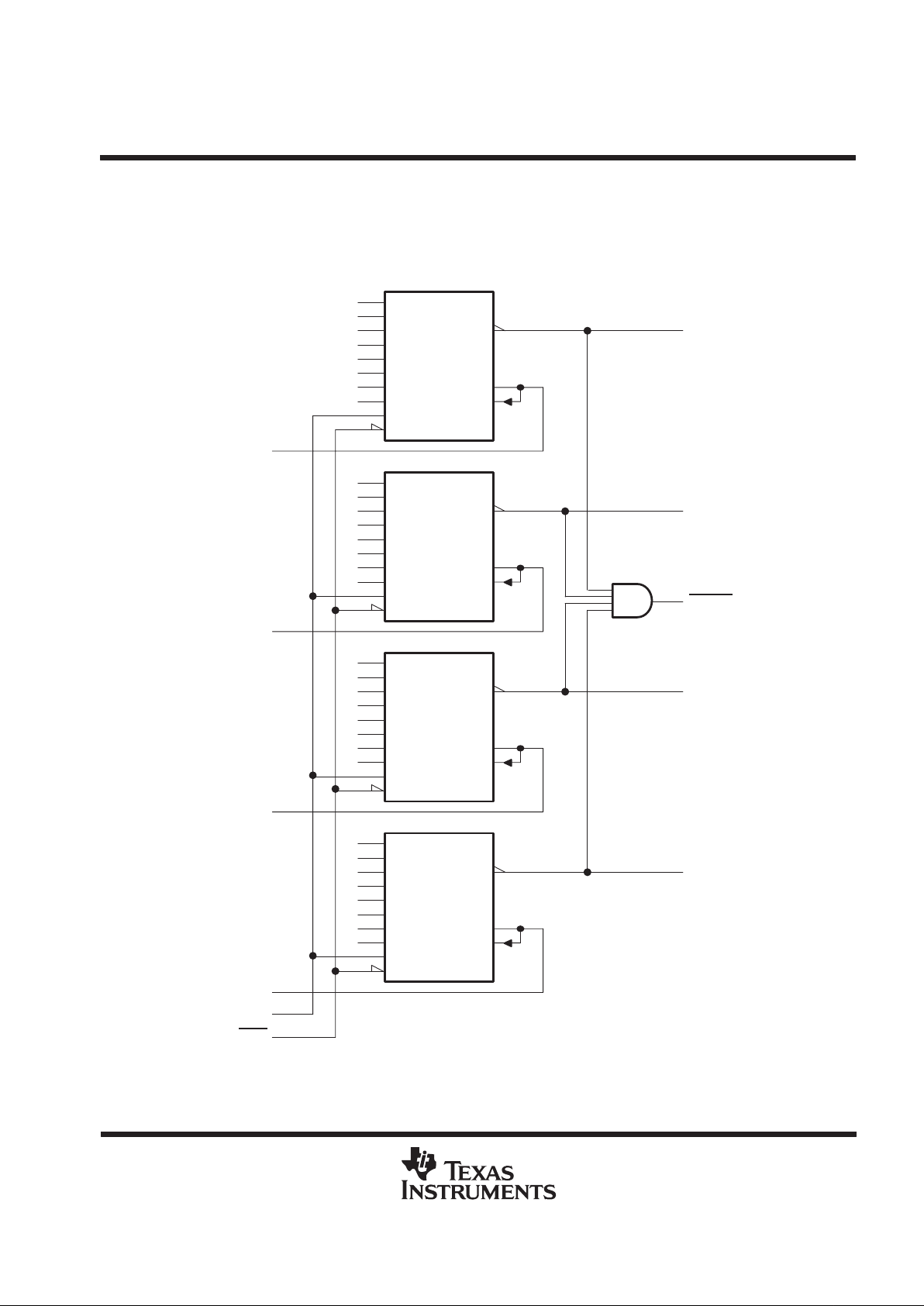
APPLICATION INFORMATION
Figure 1 shows a 32-bit parity generator/checker with output polarity switching, parity-error detection, and parity on
every byte.
A
B
C
D
E
F
G
H
I
PARITY
ERROR
XMIT
PARITY I/O
8
9
10
11
12
13
1
2
4
3
6
5
′AS286
A
B
C
D
E
F
G
H
I
PARITY
ERROR
XMIT
PARITY I/O
8
9
10
11
12
13
1
2
4
3
6
5
′AS286
A
B
C
D
E
F
G
H
I
PARITY
ERROR
XMIT
PARITY I/O
8
9
10
11
12
13
1
2
4
3
6
5
′AS286
A
B
C
D
E
F
G
H
I
PARITY
ERROR
XMIT
PARITY I/O
8
9
10
11
12
13
1
2
4
3
6
5
′AS286
EVEN/ODD
XMIT
Byte 1
Byte 2
PARITY
Byte 3
Byte 4
′AS21
Pin numbers shown are for the D, J, and N packages.
Figure 1. 32-Bit Parity Generator/Checker
Page 6
SN54AS286, SN74AS286
9-BIT PARITY GENERATORS/CHECKERS
WITH BUS-DRIVER PARITY I/O PORT
SDAS050B – DECEMBER 1983 – REVISED DECEMBER 1994
6
POST OFFICE BOX 655303 • DALLAS, TEXAS 75265
APPLICATION INFORMATION
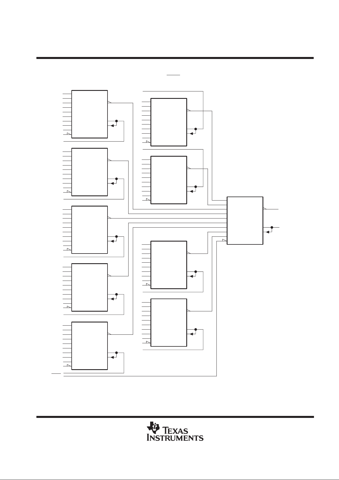
Figure 2 shows a 90-bit parity generator/checker with XMIT on the last stage available for use with parity detection.
A
B
C
D
E
F
G
H
I
PARITY
ERROR
XMIT
PARITY I/O
8
9
10
11
12
13
1
2
4
3
6
5
′AS286
A
B
C
D
E
F
G
H
I
PARITY
ERROR
XMIT
PARITY I/O
8
9
10
11
12
13
1
2
4
3
6
5
′AS286
A
B
C
D
E
F
G
H
I
PARITY
ERROR
XMIT
PARITY I/O
8
9
10
11
12
13
1
2
4
3
6
5
′AS286
A
B
C
D
E
F
G
H
I
PARITY
ERROR
XMIT
PARITY I/O
8
9
10
11
12
13
1
2
4
3
6
5
′AS286
XMIT
H
H
H
H
A
B
C
D
E
F
G
H
I
PARITY
ERROR
XMIT
PARITY I/O
8
9
10
11
12
13
1
2
4
3
6
5
′AS286
A
B
C
D
E
F
G
H
I
PARITY
ERROR
XMIT
PARITY I/O
8
9
10
11
12
13
1
2
4
3
6
5
′AS286
A
B
C
D
E
F
G
H
I
PARITY
ERROR
XMIT
PARITY I/O
8
9
10
11
12
13
1
2
4
3
6
5
′AS286
A
B
C
D
E
F
G
H
I
PARITY
ERROR
XMIT
PARITY I/O
8
9
10
11
12
13
1
2
4
3
6
5
′AS286
H
H
H
H
A
B
C
D
E
F
G
H
I
PARITY
ERROR
XMIT
PARITY I/O
8
9
10
11
12
13
1
2
4
3
6
5
′AS286
H
A
B
C
D
E
F
G
H
I
PARITY
ERROR
XMIT
PARITY I/O
8
9
10
11
12
13
1
2
4
3
6
5
′AS286
PARITY
ERROR
PARITY
I/O
Pin numbers shown are for the D, J, and N packages.
Figure 2. 90-Bit Parity Generator/Checker With Parity-Error Detection
Page 7
SN54AS286, SN74AS286
9-BIT PARITY GENERATORS/CHECKERS
WITH BUS-DRIVER PARITY I/O PORT
SDAS050B – DECEMBER 1983 – REVISED DECEMBER 1994
7
POST OFFICE BOX 655303 • DALLAS, TEXAS 75265
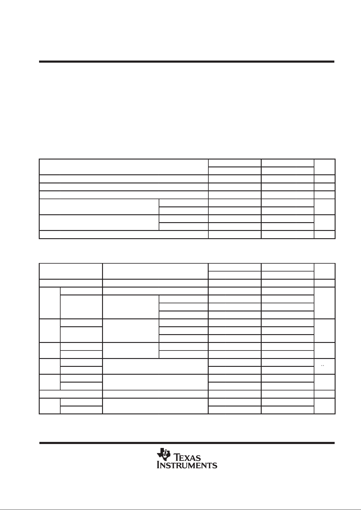
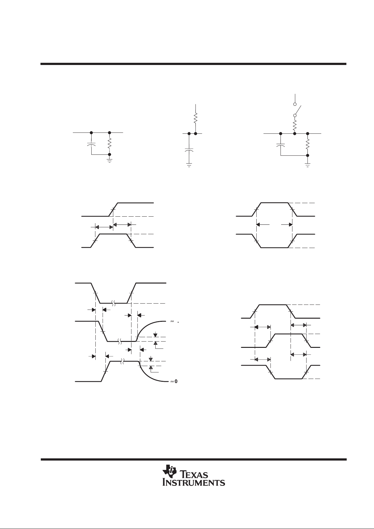
PARAMETER MEASUREMENT INFORMATION
SERIES 54ALS/74ALS AND 54AS/74AS DEVICES
t
PHZ
t
PLZ
t
PHL
t
PLH
0.3 V
t
PZL
t
PZH
t
PLH
t
PHL
LOAD CIRCUIT
FOR 3-STATE OUTPUTS
From Output
Under Test
Test
Point
R1
S1
C
L
(see Note A)
7 V
1.3 V
1.3 V1.3 V
3.5 V
3.5 V
0.3 V
0.3 V
t
h
t
su
VOLTAGE WAVEFORMS
SETUP AND HOLD TIMES
Timing
Input
Data
Input
1.3 V 1.3 V
3.5 V
3.5 V
0.3 V
0.3 V
High-Level
Pulse
Low-Level
Pulse
t
w
VOLTAGE WAVEFORMS
PULSE DURATIONS
Input
Out-of-Phase
Output
(see Note C)
1.3 V 1.3 V
1.3 V1.3 V
1.3 V 1.3 V
1.3 V1.3 V
1.3 V
1.3 V
3.5 V
3.5 V
0.3 V
0.3 V
V
OL
V
OH
V
OH
V
OL
Output
Control
(low-level
enabling)
Waveform 1
S1 Closed
(see Note B)
Waveform 2
S1 Open
(see Note B)
[
0 V
V
OH
V
OL
[
3.5 V
In-Phase
Output
0.3 V
1.3 V 1.3 V
VOLTAGE WAVEFORMS
PROPAGATION DELAY TIMES
VOLTAGE WAVEFORMS
ENABLE AND DISABLE TIMES, 3-STATE OUTPUTS
R2
V
CC
R
L
Test
Point
From Output
Under Test
C
L
(see Note A)
LOAD CIRCUIT
FOR OPEN-COLLECTOR OUTPUTS
LOAD CIRCUIT FOR
BI-STATE
TOTEM-POLE OUTPUTS
From Output
Under Test
Test
Point
C
L
(see Note A)
R
L
RL = R1 = R2
NOTES: A. CL includes probe and jig capacitance.
B. Waveform 1 is for an output with internal conditions such that the output is low except when disabled by the output control.
Waveform 2 is for an output with internal conditions such that the output is high except when disabled by the output control.
C. When measuring propagation delay items of 3-state outputs, switch S1 is open.
D. All input pulses have the following characteristics: PRR ≤ 1 MHz, tr = tf = 2 ns, duty cycle = 50%.
E. The outputs are measured one at a time with one transition per measurement.
Figure 3. Load Circuits and Voltage Waveforms
Page 8

IMPORTANT NOTICE
T exas Instruments and its subsidiaries (TI) reserve the right to make changes to their products or to discontinue
any product or service without notice, and advise customers to obtain the latest version of relevant information
to verify, before placing orders, that information being relied on is current and complete. All products are sold
subject to the terms and conditions of sale supplied at the time of order acknowledgement, including those
pertaining to warranty, patent infringement, and limitation of liability.
TI warrants performance of its semiconductor products to the specifications applicable at the time of sale in
accordance with TI’s standard warranty. Testing and other quality control techniques are utilized to the extent
TI deems necessary to support this warranty. Specific testing of all parameters of each device is not necessarily
performed, except those mandated by government requirements.
CERT AIN APPLICATIONS USING SEMICONDUCTOR PRODUCTS MAY INVOLVE POTENTIAL RISKS OF
DEATH, PERSONAL INJURY, OR SEVERE PROPERTY OR ENVIRONMENTAL DAMAGE (“CRITICAL
APPLICATIONS”). TI SEMICONDUCTOR PRODUCTS ARE NOT DESIGNED, AUTHORIZED, OR
WARRANTED TO BE SUITABLE FOR USE IN LIFE-SUPPORT DEVICES OR SYSTEMS OR OTHER
CRITICAL APPLICATIONS. INCLUSION OF TI PRODUCTS IN SUCH APPLICA TIONS IS UNDERST OOD TO
BE FULLY AT THE CUSTOMER’S RISK.
In order to minimize risks associated with the customer’s applications, adequate design and operating
safeguards must be provided by the customer to minimize inherent or procedural hazards.
TI assumes no liability for applications assistance or customer product design. TI does not warrant or represent
that any license, either express or implied, is granted under any patent right, copyright, mask work right, or other
intellectual property right of TI covering or relating to any combination, machine, or process in which such
semiconductor products or services might be or are used. TI’s publication of information regarding any third
party’s products or services does not constitute TI’s approval, warranty or endorsement thereof.
Copyright 1998, Texas Instruments Incorporated
 Loading...