

Page 1

Confidential
2002/6/26
0.2
SN11012
USB to SM/Flash Interface Controller, Mass
Storage Class Compliant
1 General Description
SN11012 is a high-performance integrated circuit to bridge USB and SM/Flash
compliance devices. It provides a flexible and cost efficient single chip solution for
external storage applications that intend to utilize the convenience of USB. To help
the system manufacturers to build high quality, low cost USB storage systems, several
special features are implemented. SN11012 can be easily configured to access SM
and/or NAND type flash devices. With supporting flash memory capability, the
combo system which supports both card reader and thumb drive can be built without
any special effort. The embedded translation table help the system makers to design a
high performance SM card or NAND type flash accessing device but still keeps the
cost low. The proprietary randomization algorithm effectively extends the lifetime of
the SM card and flash memory, ensuring the robustness of the system. The real time
ECC correction keeps the data integrity while still maintains the high data transfer
rate.
The external serial EEPROM provides the possibility to customize the USB
identity for each product. The OEM makers could make products for different
customers by just putting the vendor/product ID and names in the EEPROM but still
keep other things the same. The serial number can help the system manufacturers to
track down every single device they made even when the design and the PID/VID are
all the same. The USB Mass Storage Class compliance capability of SN11012 makes
it a truly “plug-and-play” device without vendor drivers needed under the OS like
Windows 2000/ME/XP and Mac OS 9/10. This feature not only makes the system
developing faster and easier, but also reduces the cost and increases the reliability.
The SN11012 even provides the capability to boot the PC. Therefore, the system
manufacturers can use it to build a much faster, high capacity, reliable, and portable
system to replace the legacy floppy disk easily.
1
Page 2

2002/6/26
0.2
With so many functions built-in and the high performance, easy to design-in
architecture, SN11012 is an ideal choice for building a portable USB to SM/Flash
storage system.
SN11012
Confidential
2 Features
l 12 MHz USB 1.1 full-speed compatible.
l USB 1.1 Mass Storage Class compliant
l USB Mass Storage Class Bulk-Only Transport 1.0 supported
l USB Mass Storage Class SCSI transparent command set supported
l 12 characters of serial number and up to 28 characters of
Vendor/Product/Revision string supported with external EEPROM
l Support 3.3V, 4Mbytes to 128 Mbytes SSFDC(SmartMedia Card)
l Support NAND-type flash memory, from 4Mbytes to 128 Mbytes
l Real-time ECC correction circuit to ensure the data integrity and accelerate the
access speed for SmartMedia/NAND-type flash.
l Built-in SRAM to support logical-to-physical address translation for
SmartMedia/NAND-type flash to reduce cost and increase performance and
reliability
l Supports Hot-Swapping among flash memory and SM card without un-plug
USB.
l Built-in FIFO for upstream and downstream data transfer
l Data transfer rate up to 1.5 MB/s (burst), 1.1 MB/s (read average),
l LED lightening pin available.
l PC boot up capability provided (PC BIOS needs to support USB ZIP boot up)
(version 2 only)
l No Driver needed under Microsoft Windows ME/2000/XP, Mac OS 9.x/10.x
l Driver support Microsoft Windows 98
l Single 3.3V operation
l 48 pin LQFP package.
2
Page 3
2002/6/26
0.2
SN11012
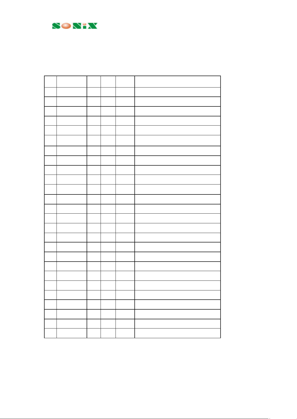
3 Pin Assignment
Pin# PAD Name Type DriveSpecial Description
1GND PWR Digital ground
2SMD6 DIO 8mA PD SM/Flash data bit 6
3SMD2 DIO 8mA PD SM/Flash data bit 2
4SMD7 DIO 8mA PD SM/Flash data bit 7
5SMD1 DIO 8mA PD SM/Flash data bit 1
6SMD0 DIO 8mA PD SM/Flash data bit 0
7SMWP DO 8mA SM/Flash write protect
8SMRB DI SM/Flash ready/busy
Confidential
9SMWE DIO 8mA PD SM/Flash write enable
10SMRE DIO 8mA PD SM/Flash read enable
11 SMALE DO 8mA SM/Flash address latch enable
12GND PWR Digital ground
13VDD PWR Digital 3.3V
14SMCLE DO 8mA SM/Flash command latch enable
15FLCE DO 8mA Flash chip enable
16NC Not Connected
17NC Not Connected
18NC Not Connected
19LED DO 8mA PD LED lighter
20RSTN DI PU Chip reset
21TEST DI PD Test pin
22SMCE DO 8mA SM chip enable
23XIN I - - Crystal input or oscillator input
24XOUT O - - Crystal output or no connection
25SMCDET DI PU SM card detect
26SMWPSW DI PU SM write protect switch
3
Page 4

SN11012
Confidential
2002/6/26
0.2
27SMPOWER DO 8mA OC SM/Flash power control
28GPIO0 DIO 8mA General Purpose Input/Output 0
29ROMCS DIO 4mA Chip select for external EEPROM
30GND PWR Digital ground
31VDD PWR Digital 3.3V
32ROMSK DIO 4mA Clock for external serial EEPROM
33ROMDI DIO 4mA Serial data to external EEPROM
34ROMDO DIO 4mA Serial data from external EEPROM
35FLCDET DI Flash card detect
36FLWPSW DI PU Flash write protect switch
37AVDD PWR analog 3.3V
38AVSS PWR analog ground
39DPLUS AIO - - USB D+ signal
40DMINUS AIO - - USB D- signal
41NC Not Connected
42NC Not Connected
43NC Not Connected
44NC Not Connected
45SMD4 DIO 8mA PD SM/Flash data bit 4
46SMD5 DIO 8mA PD SM/Flash data bit 5
47SMD3 DIO 8mA PD SM/Flash data bit 3
48VDD P - - Digital 3.3V
¨ P: power pin; AI: analog input pin, AIO: analog input/output pin; DI: digital input pin; DO: digital output
pin; DIO: digital input/output pin.
¨ TTL: TTL compatible input pin; PD: pull down; PU: pull up.
¨ All pads are Schmitt triggered and with slew rate control
4
Page 5

2002/6/26
0.2
4 Package diagram
LQPF 48 Package
F
F
L
W
P
S
W
36 35 34 33 32 3 1 3 0 29 28 27 26 25
R
R
L
O
O
C
M
M
D
D
D
E
I
O
T
SN11012
S
S
S
M
G
R
O
M
S
K
R
P
O
I
M
G
V
D
D
O
C
N
0
S
D
M
M
P
C
W
O
D
P
W
E
S
E
T
W
R
Confidential
AVDD
AVSS
DPLUS
DMINUS
NC
NC
NC
NC
SMD4
SMD5
SMD3
VDD
37
38
39
40
41
42
43
44
45
46
47
48
1 2 3 4 5 6 7 8 9 10 11 12
S
S
S
S
S
S
S
S
G
N
M
M
M
M
M
D
D
D
D
6
2
7
M
D
D
W
1
0
P
S
M
R
B
S
M
M
M
W
R
A
E
E
L
E
2 4
XOUT
2 3
2 2
2 1
2 0
1 9
1 8
1 7
1 6
1 5
1 4
1 3
G
N
D
XIN
SMCE
TEST
RSTN
LED
NC
NC
NC
FLCE
SMCLE
VDD
5
Page 6

2002/6/26
0.2
SN11012
Confidential
6
Page 7

Confidential
2002/6/26
0.2
SN11012
5 Version Control
Draft May-20-2002
0.1 June-17-2002
0.2 June-25-2002 add new feature for version 002
7
 Loading...