

Page 1
SMTPB SERIES
MAINAPPLICATIONS
Any sensitive equipment requiring protection
againstlightning strikes:
ANALOGAND DIGITALLINE CARDS
MAINDISTRIBUTIONFRAMES
TERMINALSANDTRANSMISSIONEQUIPMENT
GMS-TUBEREPLACEMENT
DESCRIPTION
TheSMTPBxxserieshasbeen designedtoprotect
telecommunication equipment against lightning
andtransient inducedby AC powerlines.
FEATURES
BIDIRECTIONALCROWBARPROTECTION.
BREAKDOWNVOLTAGERANGE:
From62 V To270V.
HOLDINGCURRENT: I
REPETITIVEPEAKPULSECURRENT :
= 100A, 10/1000µs.
I
PP
BENEFITS
= 150mA min
H
TRISIL
TM
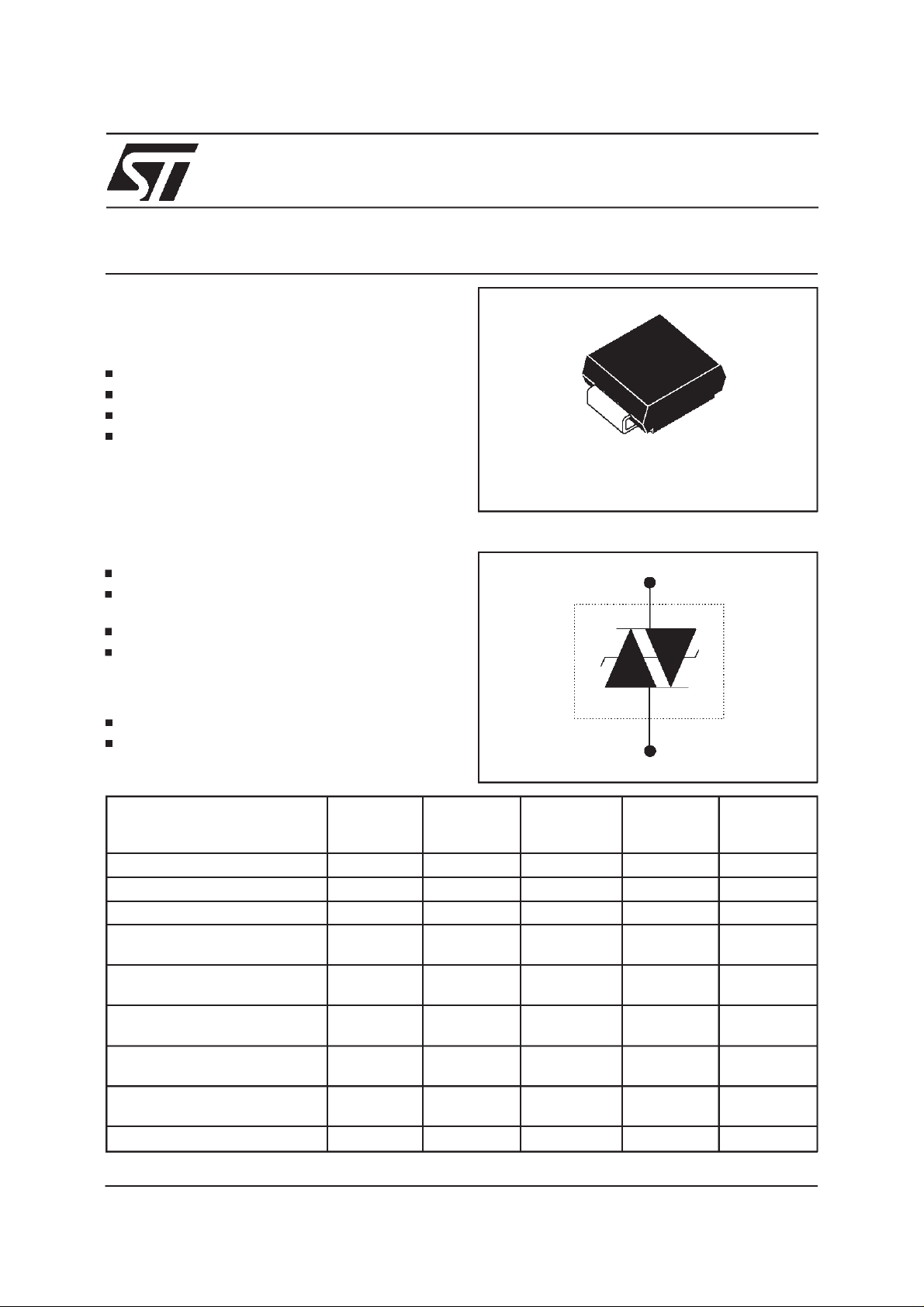
SMC
SCHEMATIC DIAGRAM
NOAGEINGANDNO NOISE
IF DESTROYED,THE SMTPBFALLS INTO
SHORTCIRCUIT, STILLENSURING
PROTECTION
COMPLIESWITHTHE
FOLLOWING STANDARDS:
CCITTK20 4000 10/700 5/310 100 VDE0433
VDE0878 4000 1.2/50 1/20 100 IEC-1000-4-5 level4
FCCPart 68, lightningsurge
typeA
FCCPart 68, lightningsurge
typeB
BELLCORETR-NWT-001089
Firstlevel
BELLCORETR-NWT-001089
Secondlevel
CNETl31-24 4000 0.5/700 0.8/310 100 -
Peak Surge
Voltage
(V)
4000 10/700 5/310 100 -
level4
1500
800
100 5/320 5/320 25 -
2500
1000
500 2/10 2/10 500 -
Voltage
Waveform
(µs)
10/700
1.2/50
10/160
10/560
2/10
10/1000
Current
Waveform
(µs)
5/310
8/20
10/160
10/560
2/10
10/1000
Admissible
Ipp
(A)
100
100
200
100
500
100
Necessary
Resistor
(Ω)
-
-
-
-
-
-
August 1999 - Ed:2C
1/5
Page 2

SMTPBxxx
ABSOLUTE MAXIMUMRATINGS (T
amb
=25°C)
Symbol Parameter Value Unit
P Powerdissipation T
I
PP
I
TSM
Peakpulse current
Nonrepetitivesurge peak on-state
=50 °C5 W
lead
10/1000µs
8/20 µs
2/10 µs
100
250
500
tp= 20ms 50 A
current
dV/dt Critical rateof riseof off-statevoltage V
T
stg
T
j
T
L
Storagetemperaturerange
Maximumjunctiontemperature
Maximumleadtemperatureforsolderingduring10 s. + 260 °C
RM
5KV/µs
- 55to +150
+ 150
THERMAL RESISTANCES
Symbol Parameter Value Unit
(j-l) Junctionto leads 20 °C/W
R
th
(j-a) Junctionto ambient.
R
th
75 °C/W
Onprinted circuitwith standardfootprintdimensions.
ELECTRICAL CHARACTERISTICS
(T
amb
=25°C)
A
°C
°C
Symbol Parameter
V
RM
I
RM
V
R
V
BR
V
BO
I
H
I
BO
I
PP
Stand-offvoltage
Leakagecurrent at stand-offvoltage
ContinuousReversevoltage
Breakdownvoltage
Breakovervoltage
Holdingcurrent
Breakovercurrent
Peakpulse current
C Capacitance
Type Marking I
RM
@V
RM
max. max.
Laser µAVµAV VmAmApF
SMT P B62
SMT P B68
SMT P B120
SMT P B200
SMT P B270
All parameters tested at 25°C,except where indicated.
W07
W11
W21
W31
W43
2
2
2
2
2
56
61
108
180
243
IR@V
note1
50
50
50
50
50
R
62
68
120
200
270
VBO@I
max.
note2
82
90
160
267
360
BO
I
H
max. min.
note3
800
800
800
800
800
150
150
150
150
150
C
typ.
note4
160
160
140
130
120
Note 1: IRmeasuredat VRguarantees V
Note 2: Measured at 50Hz (1cycle) - Seetest circuit1.
2/5
BRmin
≥ V
R
Note 3: See testcircuit 2.
Note 4: VR=1V, F = 1MHz. Refer to fig 3 forC versus VR.
Page 3

TESTCIRCUIT 1 FORIBOandVBOparameters:
Auto
Transformer
220V/2A
static
relay.
V
out
220V
Transformer
220V/800 V
5A
TESTPROCEDURE:
PulseTest duration(tp = 20ms):
-For Bidirectionaldevices= SwitchK is closed
-For Unidirectionaldevices= SwitchK is open.
V
Selection
OUT
-Devicewith V
-V
- Devicewith V
-V
BO
OUT
OUT
< 200 Volt
=250 V
≥ 200 Volt
BO
=480 V
RMS,R1
RMS,R2
= 140Ω.
=240 Ω.
= 20ms
tp
K
I
BO
measure
R1
140
R2
240
D.U.T
V
BO
measure
SMTPBxxx
TESTCIRCUIT 2 forI
parameter.
H
R
D.U.T .
V
= - 48 V
BAT
Thisis a GO-NOGOTestwhich allows to confirmthe holdingcurrent (I
testcircuit.
TESTPROCEDURE :
1) Adjustthe currentlevelat the I
valueby shortcircuiting the AKof the D.U.T.
H
2) Firethe D.U.T witha surgeCurrent: Ipp =10A , 10/1000µs.
3) TheD.U.T will come backoff-state within50 ms max.
-V
P
Surge generator
) levelin a functional
H
3/5
Page 4

SMTPBxxx
Fig.1:
Non repetitivesurgepeak on-statecurrent
versus overload duration(Tj initial=25°C).
Fig. 3: Relative variation of junction capacitance
versus reverse applied voltage(typical values).
Note: For V
upper than 56V, the curve is
RM
extrapolated(dottedline).
Fig. 2:
Relativevariationof holdingcurrentversus
junctiontemperature.
Fig. 4: On-state voltage versus on-state current
(typicalvalues).
I (A)
T
50
Tj=25°C
Fig. 5: Transient thermal impedance junction to
ambient versus pulse duration (for FR4 PC Board
withrecommendedpad layout).
10
1
2.0 2.2 2.4 2.6 2.8 3.0 3.2 3.4 3.6 3.8 4.0
V (V)T
4/5
Page 5

ORDERCODE
SMTPBxxx
SM TPB 100
SURFACE MOUNT
TRISIL PROTECTION 100 A
Marking:
Logo,datecode, typecode.
PACKAGEMECHANICAL DATA.
SMC
E1
D
E
C
L
E2
FOOTPRINTDIMENSIONS
(inmillimeters)
SMC
A2
3.3
VOLTAGE
DIMENSIONS
REF.
Millimeters Inches
Min. Max. Min. Max.
A1 1.90 2.45 0.075 0.096
A2 0.05 0.20 0.002 0.008
b 2.90 3.2 0.114 0.126
c 0.15 0.41 0.006 0.016
E 7.75 8.15 0.305 0.321
A1
E1 6.60 7.15 0.260 0.281
E2 4.40 4.70 0.173 0.185
b
D 5.55 6.25 0.218 0.246
L 0.75 1.60 0.030 0.063
Packaging:Standardpackagingisin tapeandreel
Weight: 0.25g.
2.0 4.2 2.0
Informationfurnishedis believedtobe accurate andreliable.However, STMicroelectronics assumes no responsibility for theconsequences of
use of such informationnor forany infringement of patents or otherrights of third parties which may result from its use.No license isgranted by
implication or otherwise under any patent or patent rights of STMicroelectronics. Specifications mentioned in this publication are subject to
change without notice.This publication supersedesand replacesallinformationpreviously supplied.
STMicroelectronics products are not authorized for use as criticalcomponents in lifesupport devices or systems without express written approval of STMicroelectronics.
The ST logois a registered trademark ofSTMicroelectronics
1999 STMicroelectronics - Printedin Italy - All rights reserved.
STMicroelectronics GROUP OF COMPANIES
Australia - Brazil - China - Finland - France - Germany -Hong Kong- India- Italy - Japan - Malaysia
Malta - Morocco - Singapore - Spain - Sweden - Switzerland - United Kingdom - U.S.A.
http://www.st.com
5/5
 Loading...