

Datasheet SMTPA68, SMTPA100, SMTPA120, SMTPA130, SMTPA180 Datasheet (SGS Thomson Microelectronics)
...Page 1
FEATURES
BIDIRECTIONALCROWBAR PROTECTION.
BREAKDOWNVOLTAGERANGE:
From62 V To 270 V.
HOLDINGCURRENT = 150 mA min
REPETITIVEPEAKPULSE CURRENT:
=50 A, 10/1000µs.
I
PP
DESCRIPTION
TheSMTPAxxseries hasbeen designedto protect
telecommunication equipment against lightning
andtransientinducedby AC powerlines.
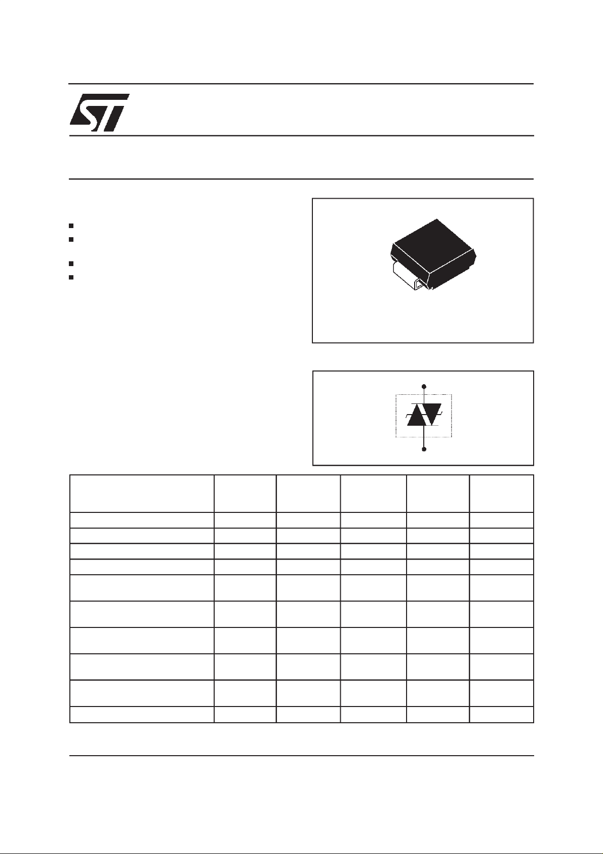
SMTPA SERIES
TRISIL
SMB
(JEDECDO-214AA)
SCHEMATIC DIAGRAM
COMPLIESWITH THE
FOLLOWINGSTANDARDS:
(CCITT)ITU-K20 1000 10/700 5/310 25 (CCITT)ITU-K17
VDE0433
VDE0878 2000 1.2/50 1/20 50 IEC-1000-4-5 level3
FCC Part 68, lightningsurge
type A
FCC Part 68, lightningsurge
type B
BELLCORETR-NWT-001089
Firstlevel
BELLCORETR-NWT-001089
Secondlevel
CNETl31-24 1000 0.5/700 0.8/310 25 -
October 1998- Ed: 7A
PeakSurge
Voltage
(V)
1500 10/700 5/310 38 2000 10/700 5/310 50 -
level4
1500
800
1000 9/720 5/320 25 -
2500
1000
5000 2/10 2/10 150 11.5
Voltage
Waveform
(µs)
10/700
1.2/50
10/160
10/560
2/10
10/1000
Current
Waveform
(µs)
5/310
8/20
10/160
10/560
2/10
10/1000
Admissible
Ipp
(A)
50
100
75
55
150
50
Necessary
Resistor
(Ω)
-
-
12.5
6.5
11.5
10
1/5
Page 2
SMTPAxxx
ABSOLUTE MAXIMUMRATINGS (T
Symbol Parameter Value Unit
P
I
PP
I
TSM
Powerdissipation
Peakpulse current 10/1000µs
Nonrepetitivesurgepeak on-state
current
dV/dt Criticalrateof rise of off-statevoltage V
T
stg
T
T
Storagetemperaturerange
Maximumjunction temperature
j
Maximumlead temperatureforsoldering during 10 s.
L
THERMAL RESISTANCES
Symbol Parameter Value Unit
Junctionto leads.
(j-l)
R
th
(j-a)
R
th
Junctionto ambienton printedcircuit
withstandardfootprintdimensions.
amb
25°C)
=
T
=50 °C5 W
lead
50
8/20 µs
100
tp= 20ms 30 A
RM
5KV/
- 55to + 150
150
260 °C
20
100 °C/W
A
s
µ
C
°
C
°
C/W
°
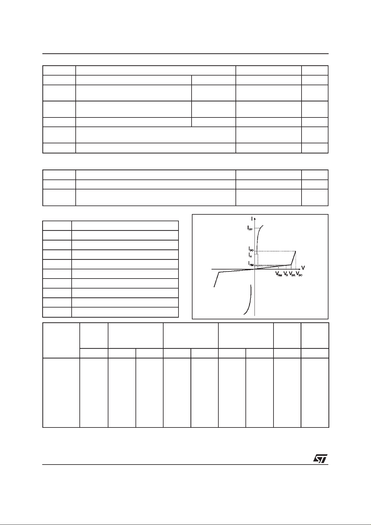
ELECTRICALCHARACTERISTICS(T
amb
Symbol Parameter
V
RM
I
RM
V
V
BR
V
BO
I
H
I
BO
I
PP
C
Type Marking I
Stand-offvoltage
Leakagecurrentat stand-offvoltage
ContinuousReversevoltage
R
Breakdownvoltage
Breakovervoltage
Holdingcurrent
Breakovercurrent
Peak pulse current
Capacitance
@V
RM
RM
max. max.
Laser
SMTPA62
SMTPA68
SMTPA100
SMTPA120
SMTPA130
SMTPA180
SMTPA200
SMTPA220
SMTPA240
SMTPA270
Allparameters tested at 25°C, except whereindicated.
Note 1: IRmeasured at VRguaranteeV
Note 2: Measured at 50Hz(1 cycle) - See testcircuit 1.
U01
U05
U13
U17
U19
U25
U27
U31
U35
U39
AV
µ
2
2
2
2
2
2
2
2
2
2
BRmin
56
61
90
108
117
162
180
198
216
243
V
≥
R
=25°C)
note 1
IR@V
AV VmAmApF
µ
50
50
50
50
50
50
50
50
50
50
R
62
68
100
120
130
180
200
220
240
270
Note 3: See testcircuit 2.
Note 4: VR= 1V,F = 1MHz. Refer to fig.3 for C versus VR.
VBO@I
max.
note2
82
90
133
160
173
240
267
293
320
360
BO
I
H
max. min.
note3
800
800
800
800
800
800
800
800
800
800
150
150
150
150
150
150
150
150
150
150
C
max.
note4
150
150
100
100
100
100
100
100
100
100
2/5
Page 3

TESTCIRCUIT 1 FORIBOandVBOparameters:
Auto
Transformer
220V/2A
static
relay.
V
out
220V
Transformer
220V/800V
5A
TESTPROCEDURE:
PulseTest duration (tp = 20ms):
- For Bidirectional devices = SwitchK is closed
- For Unidirectionaldevices = Switch K is open.
V
Selection
OUT
- Device with V
-V
- Devicewith V
-V
OUT
BO
OUT
BO
200 Volt
<
=250 V
≥ 200Volt
= 480 V
RMS,R1
RMS,R2
= 140Ω.
= 240Ω.
= 20ms
tp
K
I
BO
measu re
R1
140
R2
240
D.U.T
V
BO
measure
SMTPA xxx
TESTCIRCUIT 2 forI
V
= - 48 V
BAT
Thisis a GO-NOGOTestwhich allowsto confirm the holdingcurrent (I
testcircuit.
TESTPROCEDURE :
1) Adjustthe currentlevel at theI
2) Firethe D.U.T with a surgeCurrent: Ipp = 10A , 10/1000 µs.
3) TheD.U.T will come backoff-state within 50ms max.
parameter.
H
R
D.U.T .
Surge generator
) levelin a functional
H
valueby short circuitingthe AK of the D.U.T.
H
-V
P
3/5
Page 4

SMTPAxxx
Fig.1: Non repetitivesurge peak on-statecurrent
versus overload duration(Tj initial=25°C).
(A)
TSM
Fig. 3: Relative variation of junction capacitance
versus reverse applied voltage (typical values).
Note: For VRMupper than 56V, the curve is ex-
trapolated(dotted line).
Fig. 2: Relativevariation of holdingcurrent versus
junctiontemperature.
Fig. 4: On-state current versus on-state voltage
(typicalvalues).
I (A)T
V (V)R
Fig. 5: Transient thermal impedance junction to
ambient versus pulse duration (for FR4 PC Board
withT
4/5
= 10 mm).
lead
tp(s)
V (V)T
Page 5

SURFACE MOUNT
SMTPA xxx
SM TPA 100
TRISIL PROTECTION 50 A
MARKING : Logo,date code, type code.
PACKAGEMECHANICAL DATA.
SMB (JEDEC DO-214AA)
E1
D
E
A1
C
L
A2
FOOTPRINTDIMENSION(in millimeters)
SMB
VOLTAGE
DIMENSIONS
REF.
Millimeters Inches
Min. Max. Min. Max.
A1 1.90 2.45 0.075 0.096
A2 0.05 0.20 0.002 0.008
b 1.95 2.20 0.077 0.087
c 0.15 0.41 0.006 0.016
E 5.10 5.60 0.201 0.220
E1 4.05 4.60 0.159 0.181
D 3.30 3.95 0.130 0.156
b
L 0.75 1.60 0.030 0.063
Packaging:
Standardpackagingis in tape and reel
Weight: 0.12g
2.3
1.52 2.75
Informationfurnished is believed to be accurateand reliable. However, STMicroelectronics assumes no responsibilityfor theconsequences of
use of such informationnor forany infringementof patentsor other rightsof thirdparties which may result from its use. No license is granted by
implication or otherwise under any patent or patent rights of STMicroelectronics. Specifications mentioned in this publication are subject to
change without notice. This publication supersedes and replaces all information previously supplied.
STMicroelectronics products are not authorized for use as critical components in life support devices or systems without express written approval of STMicroelectronics.
Australia - Brazil - Canada - China - France - Germany - Italy - Japan - Korea - Malaysia - Malta - Mexico - Morocco -
The Netherlands - Singapore - Spain - Sweden - Switzerland - Taiwan - Thailand - United Kingdom - U.S.A.
1.52
The ST logo is a registeredtrademark of STMicroelectronics
1998 STMicroelectronics - Printed in Italy - All rights reserved.
STMicroelectronics GROUP OF COMPANIES
http://www.st.com
5/5
 Loading...