

Page 1
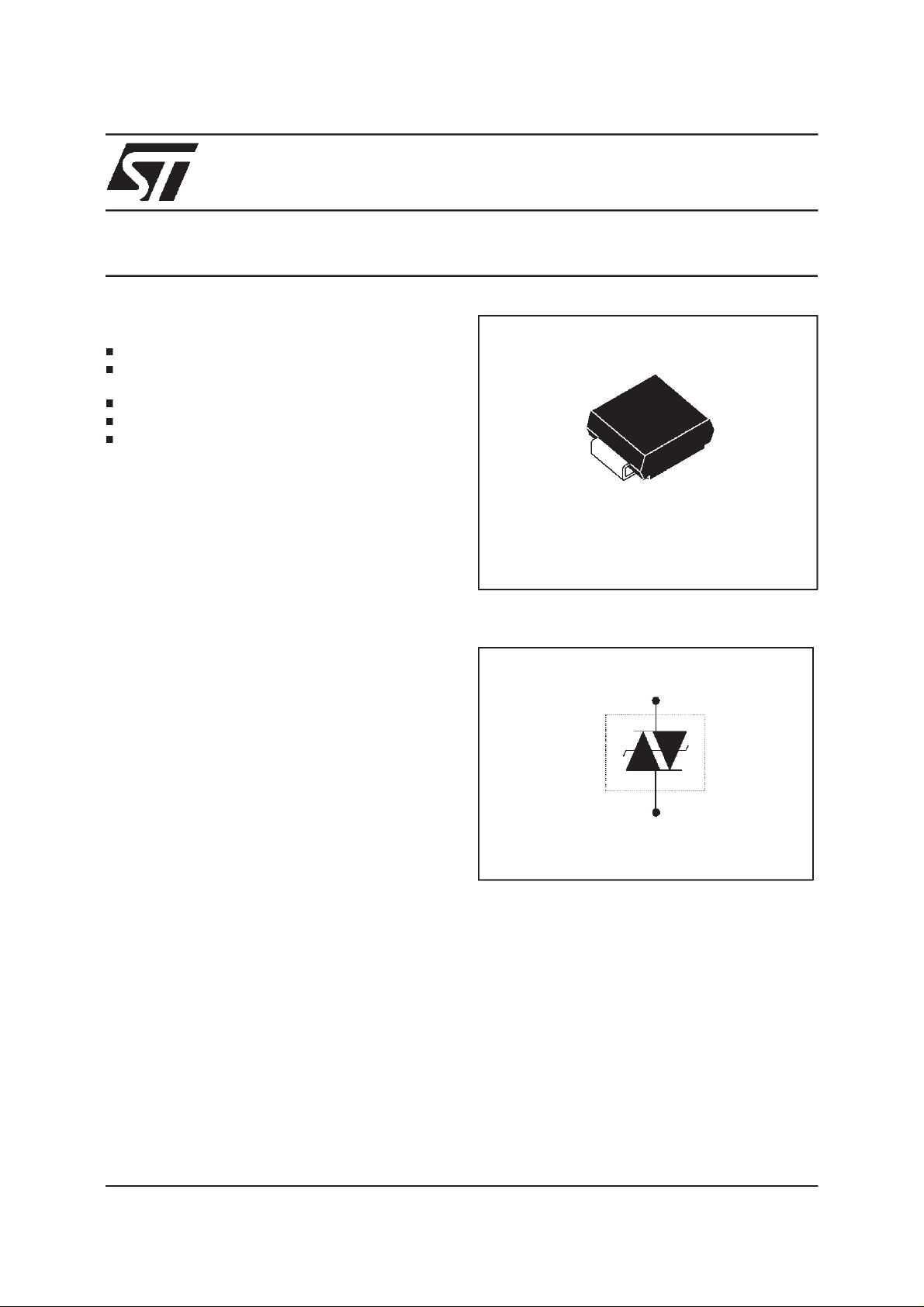
SMTHBT200
TRISIL
FEATURES
BIDIRECTIONALCROWBARPROTECTION
REPETITIVEPEAK PULSECURRENT:
= 100 A (10/1000µs)
I
PP
HOLDINGCURRENT: I
BREAKDOWNVOLTAGE: 200V min
BREAKOVERVOLTAGE: 265Vmax
DESCRIPTION
This protection device h as been especially
designed to protect subscriber line cards using
SLICS without int egrated ring generators.
The SMTHBT200 device protects ring
generat or relays against transient
= 150 mA
H
TM
FOR LINE CARD PROTECTION
SMC
SCHEMATIC DIAGRAM
INACCORDANCEWITHTHEFOLLOWINGSTANDARDS :
- CCITTK20: 10/700µs4kV
5/310µs 100 A
- VDE 0433: 10/700µs4kV
5/310µs 100 A
- VDE 0878: 1.2/50µs4kV
1/20µs 100A
- FCC Part68: 2/10µs 2.5 kV
BELLCORETR-NWT-001089: 2/10µs 500A
- BELLCORETR-NWT-000974:10/1000µs1kV
10/1000µs 100A
August 1999-Ed : 3A
1/6
Page 2
SMTHBT200
THERMAL RESISTANCES
Symbol Parameter Value Unit
R
R
th(j-I)
th(j-a)
Junctionto leads 10 °C/W
Junctionto ambienton printedcircuit
75 °C/W
(withstandardfootprint dimensions)
ABSOLUTE MAXIMUMRATINGS
(T
=
25°C,unless otherwisespecified)
amb
Symbol Parameter Value Unit
I
pp
I
TSM
dV/dt
T
T
stg
Tj
Note 1:
L
Peakpulse current:
10/1000µs (open circuitvoltagewaveform 10/1000µs)
8/20µs (opencircuitvoltage waveform4kV 1.2/50µs)
Nonrepetitivesurge peak on-statecurrent
Critical rateof riseof off-statevoltage
tp = 20ms
V
RM
100
250
55 A
Maximumlead temperaturefor solderingduring 10s 260 °C
Storagetemperaturerange
Maximumjunction temperature
Pulsewaveform
%I
PP
- 55to +150
150
5 KV/µs
A
A
°C
°C
µ
10 / 1000µstr=10µs tp = 1000
s
8/20µstr=8µstp=20µs
5 / 310µstr=5µs tp = 310µs
1/20µstr=1µstp=20µs
2/10µstr=2
µ
stp=10
µ
s
100
50
0
t
rp
t
2/6
Page 3

SMTHBT200
ELECTRICALCHARACTERISTICS(T
amb
=25°C)
Symbol Parameter
V
RM
I
RM
V
R
V
BR
V
BO
I
H
I
BO
I
PP
C
Stand-offvoltage
Leakagecurrentat stand-offvoltage
ContinuousReverse voltage
Breakdownvoltage
Breakovervoltage
Holdingcurrent
Breakovercurrent
Peak pulse current
Capacitance
STATICPARAMETERS
Type
@V
I
RM
RM
max.
AV
µ
I
@V
R
R
max.
note1
AV VmAmAmA pF
µ
V
BO
max. min.
max. note2
@I
BO
I
H
min.
note3
SMTHBT200 10 180 50 200 265 150 800 150 150
C
max.
note4
Note 2 : IRmeasured at VRguaranteesVBR>V
Note 2 : Measured at 50Hz, see testcircuit 1.
Note 3 :
See functionalholding current test circuit2.
Note 4 :
VR=1V bias, V
=1V, F=1MHz.
RMS
R
3/6
Page 4

SMTHBT200
TESTCIRCUIT 1 FORI
Auto
Transformer
220V/2A
220V
TESTPROCEDURE :
PulseTest duration(tp =20ms):
-For Bidirectionaldevices= SwitchK isclosed
-For Unidirectionaldevices = SwitchK is open.
V
Selection
OUT
-Device with V
-V
OUT
- Devicewith V
-V
OUT
andVBOparameters:
BO
V
Transformer
220V/800V
5A
< 200 Volt
BO
= 250V
≥ 200 Volt
BO
=480 V
,R1= 140Ω.
RMS
RMS,R2
static
relay.
out
=240Ω.
= 20ms
tp
K
I
BO
measure
R1
140
R2
240
D.U.T
V
BO
measure
TESTCIRCUIT2 for IHparameter.
R
-V
P
V
BAT
D.U.T.
= - 48 V
Surge generator
This is a GO-NOGO testwhich allows to confirmthe holdingcurrent (IH)level in a functionaltest circuit.
TESTPROCEDURE:
- Adjust the currentlevel at the I
- Firethe D.U.T. witha surgecurrent: I
- TheD.U.T. will comeback to the off-statewithin 50 ms max.
4/6
value by short circuiting the D.U.T.
H
=10A, 10/1000µs.
pp
Page 5

SMTHBT200
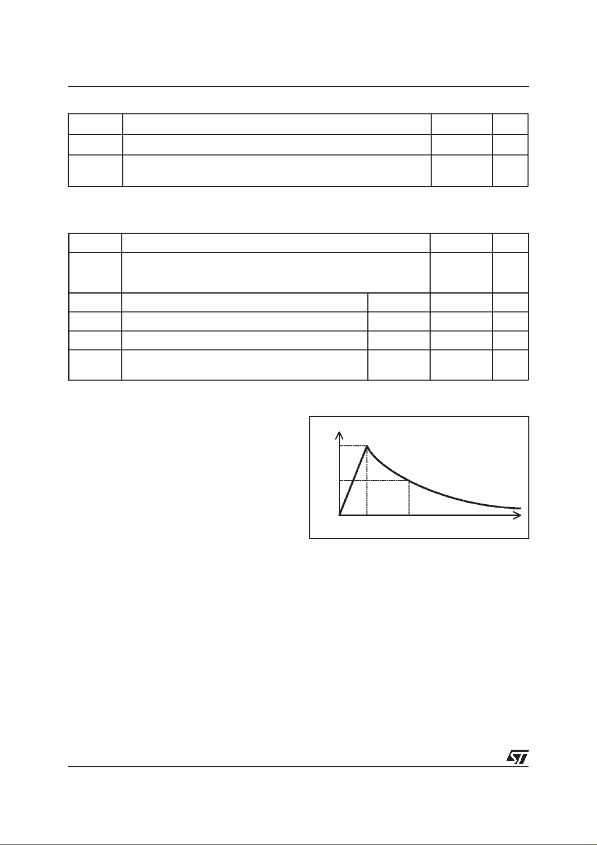
Fig 1 :
versusoverloadduration(T
70
60
50
40
30
20
10
Fig 3 :
Non repetitivesurge peak on-state current
initial= 25 °C).
j
I (A)TSM
F=50Hz
0
1E-2 1E-1 1E+0 1E+1 1E+2 1E+3
t(s)
Relativevariation of holdingcurrent versus
junctiontemperature.
IH[Tj] / IH[Tj=25°C]
2.0
1.8
1.6
1.4
1.2
1.0
0.8
0.6
0.4
0.2
0.0
-40 -20 0 20 40 60 80 100 120
j
T(°C)
Fig 2 :
On-state voltage versus on-state current
(typicalvalues).
I (A)
T
50
Tj=25°C
10
1
2.0 2.2 2.4 2.6 2.8 3.0 3.2 3.4 3.6 3.8 4.0
Fig 4 :
Variation of thermal impedancejunction to
V (V)T
ambientversuspulse duration.
Zth(j-a)(°CW)
100
10
1
1E-3 1E-2 1E-1 1E+0 1E+1 1E+2 5E+2
t (s)p
Fig 5 :
Relative variation of junction capacitance
versusreversevoltageapplied (typicalvalues).
Note : For VBR upper than 62 V, the curve can be extrapolated
(dottedline)
C[VR]/C[VR=1V]
1.0
F=1MHz
0.5
0.2
0.1
1 10 100 300
V (V)R
5/6
Page 6

SMTHBT200
PACKAGEMECHANICAL DATA
SMC(Plastic)
E1
D
E
C
L
E2
DIMENSIONS
REF.
Millimeters Inches
Min. Max. Min. Max.
A1 1.90 2.45 0.075 0.096
A2 0.05 0.20 0.002 0.008
b 2.90 3.2 0.114 0.126
c 0.15 0.41 0.006 0.016
E 7.75 8.15 0.305 0.321
E1 6.60 7.15 0.260 0.281
A1
A2
b
E2 4.40 4.70 0.173 0.185
D 5.55 6.25 0.218 0.246
L 0.75 1.60 0.030 0.063
FOOTPRINT
(in millimeters)
3.3
Packaging
MARKING
: tapeand reel
Package Type Marking
SMC SMTHBT200 WO4
2.0 4.2 2.0
Informationfurnished is believedto beaccurate and reliable. However, STMicroelectronics assumesno responsibility for the consequences of
use of such information nor forany infringementof patents or other rights of third parties which may resultfrom itsuse. Nolicense is granted by
implication or otherwise under any patent or patent rights of STMicroelectronics. Specifications mentioned in this publication are subject to
change without notice. This publicationsupersedes and replacesall information previously supplied.
STMicroelectronics products are not authorized for use as critical components in life support devices or systems without express written
approval of STMicroelectronics.
The ST logois a registeredtrademark of STMicroelectronics
1999 STMicroelectronics - Printedin Italy - All rights reserved.
STMicroelectronics GROUP OF COMPANIES
Australia - Brazil - China - Finland - France - Germany - Hong Kong - India - Italy - Japan - Malaysia
Malta - Morocco - Singapore - Spain - Sweden - Switzerland - United Kingdom -U.S.A.
http://www.st.com
6/6
 Loading...