

Page 1
SUMMIT
MICROELECTRONICS, Inc.
Quad Power Supply Controller
FEATURES DESCRIPTION
SMT4004
l Programmable Voltage and Current Monitoring
w Monitors 4 independent supplies
w Programmable Host-side Under- and Over-
Voltage Thresholds
w Programmable Card-side Under-Voltage
Monitors
w Programmable Card-side Circuit Breaker
Delay and QuickTrip™ Threshold Levels
l Programmable Card-side Trakker Function
w Programmable Slew Rate Control
w Guarantees and Enforces Supply Differential
Tracking
l Programmable Watchdog and Longdog Timers
(0 to 6.4 seconds)
l Operates From Any One of Four Supply Voltages
l Nonvolatile Fault Register
w Records Source of Any Interrupt
w Readable in “Dead Board” Environment
l All Communications to Configuration Registers
and Memory Array are via I2C Interface
The SMT4004 is a fully integrated programmable voltage
manager IC, providing supervisory functions and tracking
control for up to four independent power supplies. The
four internal managers perform the following functions:
Monitor source (bus-side) voltages for under- and overvoltage conditions, monitor each supply for over-current
conditions, monitor back end (card-side) voltages for two
staged levels of under-voltage conditions, insure power to
the card-side logic tracks within the specified parametric
limits, and provide supply status information to a host
processor.
The SMT4004 incorporates nonvolatile programmable
circuits for setting all of the monitored thresholds for each
manager. Individual functions are also programmable
allowing interrupts or reset conditions to be generated by
any combination of events. Because of a proprietary
EEPROM technology that it employs it is also able to store
fault conditions as they occur. In the case of a catastrophic
failure the fault is recorded in the registers and then can be
read for analysis.
Programming of configuration, control and calibration
values by the user can be simplified with the interface
adapter and Windows GUI software obtainable from Summit Microelectronics.
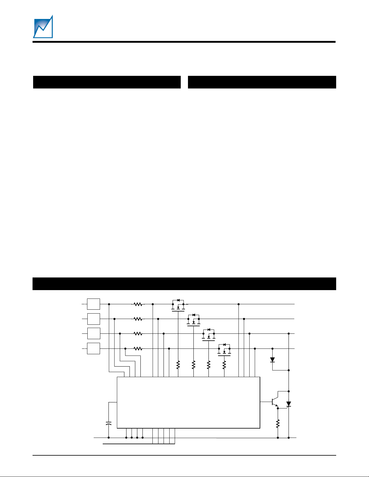
SIMPLIFIED APPLICATION DIAGRAM
5V
3.3V
2.5V
1.8V
OPTIONAL
VI1
VI2
VI3
VI4
CB1
CB2
VDD_CAP
SDA
GND4
SCLA0A1
GND1
GND2
GND3
I2C
©SUMMIT MICROELECTRONICS, Inc., 2001 • 300 Orchard City Dr., Suite 131 • Campbell, CA 95008 • Phone 408-378-6461 • FAX 408-378-6586 • www.summitmicro.com
VG1
CB3
CB4
SMT4004
A2
VG2
VG3
GND
VG4
CROWBAR
VO1
CROWBAR
VO2
VO3
VO4
100Ω
Characteristics subject to change without notice 2049 3.1 3/19/01
1
Page 2
FUNCTIONAL BLOCK DIAGRAM
SMT4004
UV_OVERRIDE
VO1
CB1
VI1
VO2
CB2
VI2
VO3
CB3
VI3
VO4
CB4
VI4
PWR_ON
12
20
37
41
21
36
40
22
35
39
23
34
38
SUPPLY
MANAGER
#1
SUPPLY
MANAGER
#2
SUPPLY
MANAGER
#3
SUPPLY
MANAGER
#4
33
FORCE_SD
27
SEQUENCE
ENABLE
LOGIC
All Resistors
are 100kΩ
SEATED1#
SEATED2#
10
11
MR#
IRQ_CLR#
5
RESET &
STATUS
OUTPUT
CONTROL
LOGIC
CHARGE
PUMP &
VGATE
CONTROL
TRAKKER
LOGIC
TIMER
LOGIC
6
IRQ#
7
RST1#
13
14
RST2#
RST3#
15
16
RST4#
CROWBAR
3
CBFAULT
25
HEALTHY#
26
VGATE1
32
VGATE2
31
VGATE3
30
VGATE4
29
VGG_CAP
28
ENABLE
24
TRKR_IRQ#
9
48
WLDI
1
LDO#
2
WDO#
REF
4
A0
43
A1
44
A2
45
SDA
46
SCL
47
2049 BD 2.2
42
VDD_CAP
2049 3.1 3/19/01
POWER
SUPPLY
ARBITRATION
8
PGND
18
DGND
19
AGND
MEMORY
& 2-WIRE
BUS
INTERFACE
17
PGND
SUMMIT MICROELECTRONICS, Inc.
1.25V
2
Page 3
PIN CONFIGURATION
WLDI
SCL
48-Pin TQFP
SDAA2A1A0V
_CAP
DD
VI1
VI2
VI3
VI4
SMT4004
CB1
LDO#
WDO#
CROWBAR
1.25V
REF
MR#
IRQ_CLR#
IRQ#
PGND
TRKR_IRQ#
SEATED1#
SEATED2#
UV_OVERRIDE
4847464544434241403938
1
2
3
4
5
6
7
8
9
10
11
12
1314151617181920212223
VO1
PGND
DGND
RST1#
RST2#
RST3#
RST4#
AGND
VO2
VO3
37
36
35
34
33
32
31
30
29
28
27
26
25
24
VO4
ENABLE
CB2
CB3
CB4
PWR_ON
VGATE1
VGATE2
VGATE3
VGATE4
VGG_CAP
FORCE_SD
HEALTHY#
CBFAULT
2049 PCon 2.1
ABSOLUTE MAXIMUM RATINGS*
Temperature Under Bias .......................-55°C to 125°C
Storage Temperature ............................-65°C to 150°C
Lead Solder Temperature (10 secs) ...................300 °C
Terminal Voltage with Respect to GND:
V0, V1, V2, and V3........... -0.3V to 6.0V
All Others........................ -0.3V to 6.0V
RECOMMENDED OPERATING CONDITIONS
Temperature –40ºC to 85ºC.
Voltage 2.7V to 5.5V
SUMMIT MICROELECTRONICS, Inc.
2049 3.1 3/19/01
*COMMENT
Stresses listed under Absolute Maximum Ratings may cause permanent damage to the device. These are stress ratings only, and
functional operation of the device at these or any other conditions
outside those listed in the operational sections of this specification is not
implied. Exposure to any absolute maximum rating for extended
periods may affect device performance and reliability.
3
Page 4
DC OPERATING CHARACTERISTICS
(Over Recommended Operating Conditions; Voltages are relative to GND)
lobmySretemaraPsetoN.niM.pyT.xaMstinU
IV4IVhguorht1IVsegatlovylppuS
I
nO
DD
ffOevitcaniELBANE1.0Am
I
DD
P
TIV
IV
SYH
V
BC
BC
YALED
V
BCQ
V
FER
nO
V
GV
ffOGV
V
GV
I
GV
RS
GV
RS
ATLED
P
TVO
VO
SYH
V
HI
V
LI
V
LO
t
WORC
egnar
V52.1
FER
tnerrucylppusrewoP
dlohserhttupniIVelbammargorP
siseretsyhpirtVU/VO 01Vm
egatlovpirtrekaerbtiucriC515204Vm
retliftnerruc-revO
egatlovpirt-kciuQ
.g.e
(
egatlovtuptuoR
egatlovtuptuoevirdETAGV
tnerructuptuoevirdETAGVnOsehctiwsTEFSOM08Aµ
etarwelsegatlovtuptuoETAGV
laitnereffidwelsREKKART
egatlovedis-dracelbammargorP
egnardlohserht
siseretsyhtupniVO 01Vm
egatlovhgihtupnI
egatlovwoltupnI
stuptuoniardnepOI
KNIS
htdiwesluptuptuorabworCk1otni.nimV5.2 Ω 6182sµ
(IVtsehgiH ≥ ehtsrewop)V7.2
4004TMS
evitcaELBANEdnaNO_RWP13Am
tib/Vm02,noitulosertib-89.00.6V
.elbammargorP
,0D&1Dstibatad
ylevitcepser
.elbammargorP
6D&7Dstibatad
ylevitcepser,)
k2= Ω 32.152.172.1V
DAOL
00 52sµ
01 05sµ
,B1RretsigeRybteS
10 001sµ
11 002sµ
00 ffO
01 57Vm
,A1RretsigeRybteS
10 001Vm
11 051Vm
nOsehctiwsTEFSOM4161V
Am1=04.0V
KNIS
.elbammargorP
00 04001041s/V
01 001052053s/V
,01RretsigeRybteS
ro2D&3Dstibatad
10 002005007s/V
ylevitcepser,0D&1D
11 00400010041s/V
laitnereffidatled,snipOV
dewolla
tib/Vm02,noitulosertib-89.00.6V
V7.2=IV9.0 × IVIVV
V5=IV7.0 × IVIVV
V7.2=IV1.0– 1.0 × IVV
V5=IV1.0– 3.0 × IVV
Am2=04.0V
SMT4004
7.25.5V
001Vm
2049 Elect Table 1.1
4
2049 3.1 3/19/01
SUMMIT MICROELECTRONICS, Inc.
Page 5

PIN DESCRIPTIONS AND DEVICE OPERATION
THE
TRAKKER
SUPPLY VOLTAGES
SMT4004
SUPPLY MANAGERS
The VI inputs of all four supply managers are diode ORed
and tied to the device's internal VDD node. The
will use the highest VI input for its supply voltage. At least
one VI input must be at or above 2.7V for proper device
operation.
VDD_CAP — Charge storage connection for the chip's
internal power supply. For most applications a 10µF
capacitor should be connected to his pin.
VGG_CAP — This pin should be tied to a capacitor to be
charged by the charge pump. The capacitor should be of
sufficient size so as to provide current to the VGATE
outputs under varying load conditions.
PGND — Power ground
DGND — Digital Ground
AGND — Analog Ground
TRAKKER
TIMERS
LDO# — The longdog timer output is an active-low open-
drain output that can be wire-ORed with other open-drain
signals. The longdog timer is generally programmed to
generate an output at a time interval longer than the
watchdog timer. The time interval is programmed in
Register
WDO# — The watchdog timer output is an active-low
open-drain output that can be wire-ORed with other opendrain signals. The watchdog timer is generally programmed to generate an output at a time interval shorter
than the longdog timer. The time interval is programmed
in Register
R1C
R1C
.
.
The electrical placement of the SMT4004 on a printed
circuit card is such that it separates the host power supply
and any on-board DC-to-DC converters (or LDOs) from
the backend circuitry such as multiple DSPs, microprocessors and associated glue logic. The host supplies, and
any other regulated voltages that will be “switched” by the
device, are referred to as bus-side voltages. The voltages
that are on the backend circuitry side of the switches are
referred to as card-side voltages.
The four supply manager blocks are identical. Each
contains three primary functional blocks: the first monitors
the bus-side voltages, the second monitors the card-side
voltages, and the third monitors over-current conditions
for that particular supply.
BUS-SIDE MANAGEMENT
Figure 1 illustrates the functional blocks of the four supply
managers. Each manager block can be independently
enabled or electrically removed from the device.
The VI input monitors the bus-side voltage for both undervoltage and over-voltage conditions. The thresholds for
the under-voltage detection for VI inputs are programmed
in Registers
the V
designed so that the threshold can be determined by
multiplying the binary value of the Register times 20mV
and adding that to 0.9V in the formula P
× n), where n is the register value (0 - 255 decimal). This
allows very precise monitoring of voltages in the range of
0.9V to 6V without the use of external resistor divider
networks.
R00
through
of a nonvolatile DAC. The DAC has been
REF
R03
. The VI input is effectively
= 0.9V + (0.2mV
VIT
WLDI — Watchdog and longdog timer reset input. A low-
to-high transition on this pin will reset both the watchdog
timer and the longdog timer.
The watchdog and longdog work in tandem: resetting one
resets the other. Generally, the longdog will be programmed to time out sometime after the watchdog. As an
example, the WDO# output could be used to generate a
warning interrupt and the LDO# output could be tied to a
system reset line.
Both timers can be turned off, facilitating system debug
and also allowing operating systems to ‘boot up’ and
configure themselves without interrupts or resets.
SUMMIT MICROELECTRONICS, Inc.
2049 3.1 3/19/01
The over-voltage level is determined by the value in
registers
SMT4004 GUI. All enabled manager blocks must ensure
their respective VI inputs are within the programmed limits
before the VGATE outputs can be turned on and the
TRAKKER
also be used to generate a general interrupt.
It should be noted that either one or both of the bus-side
monitors could be disabled via Registers
R07
R04
through
logic enabled. The VI comparator outputs can
.
R07
, and is selected by the
R04
through
5
Page 6
SMT4004
VI
X
CB
VO
–
+
+
V
REF
X
X
Programmable
Delay
Programmable
Quick Trip
Threshold
25mV
–
+
–
+
–
Comparator
–
+
OV
Comparator
UV
Comparator
Circuit
Breaker
Comparator
Quick
Trip
UV1
Comparator
Quick Trip
OC
VGATE Enable
( = Programmable)
To IRQ
VGATE and
TRAKKER
Logic
To Crowbar
To RST
+
V
REF
–
UV2
Comparator
Figure 1. Supply Manager Circuit
CARD-SIDE MANAGEMENT
On the card-side the
mable under-voltage thresholds on the VO inputs: UV1
and UV2. UV1 can be used to generate a warning interrupt
that the supply is decaying, and UV2 can be used to
generate a reset condition or a crowbar output. The cardside under-voltage (UV1) threshold value is programmed
in Registers R08 through R0B. Like the bus-side thresholds the levels can be programmed in 20mV increments
(on top of 0.9V). The second level (UV2) is determined by
6
TRAKKER
monitors two program-
2049 3.1 3/19/01
2049 Fig01 1.0
the value in Registers R0C through R0F, and is selected
by the SMT4004 GUI.
It should be noted that either one or both of the card-side
monitors can be disabled via Registers
R0C
through
R0F
OVER-CURRENT PROTECTION
The CB inputs are the circuit breaker inputs for the supply
voltages. With a series resistor placed in the supply path
between VI and CB the circuit breaker will trip whenever
the voltage across the resistor exceeds 25mV.
SUMMIT MICROELECTRONICS, Inc.
.
Page 7

SMT4004
The on-board electronic circuit breaker can be programmed to application specific levels. The circuit
breaker delay defines the period of time the voltage drop
across RS is greater than 25mV but less than V
QCB
before
the VGATE output will be shut down. This is effectively a
filter to prevent spurious shutdowns of VGATE. The
delays that can be programmed are 25µs, 50µs, 100µs
and 200µs. The programmable delay bits are located in
Register
The Quick-Trip circuit breaker threshold (V
to 150mV, 100mV, 75mV or off (Register
R1B
.
) can be set
QCB
R1A
). This is the
threshold voltage drop across RS that is placed between
V
and CBSENSE. If the voltage drop exceeds the
SS
programmed threshold, the electronic circuit breaker will
immediately trigger with no delay.
The outputs of these comparators can be used to generate
interrupts and reset conditions and toggle the crowbar
output.
POWER-ON SEQUENCING
In order to begin sequencing of the card-side supplies
(ramping the VGATE outputs) a number of conditions
must be met. All enabled bus-side voltages must be above
their respective under-voltage thresholds, the card-side
voltages (
be near zero volts, and the following inputs must be
properly set.
ENABLE — When active the ENABLE input brings
the IC out of a standby mode where the charge pump
supplying the VGATE outputs is turned on (and
begins charging the VGG_CAP) and the bandgap
reference is turned on. The ENABLE input can be
programmed to be either active low (default from the
factory) or active high (Register
SEATED1# and SEATED2# — the SEATED inputs
are effectively two additional enable inputs that must
be low to enable the sequencing of the card-side
voltages. In a staggered pin environment these
inputs can be tied to the “short” pins, insuring the card
is fully seated before any power is applied to the cardside logic. These inputs can also be tied to card
insertion switches to indicate proper seating.
PWR_ON — the PWR_ON input is the last input that
will typically be driven to enable power sequencing to
the card-side. The PWR_ON input can be programmed to be either active low (default from the
factory) or active high (Register
e.g.
, residual capacitor stored potentials) must
R1B
).
R1B
).
TRAKKING
AND SOFTSTART CONTROL
VGATE — The VGATE outputs are used to control the
“turning-on” of the card-side voltages. The ramp rate (for
both turn-on and turn-off) of the outputs is programmable
from 100V/s to 1000V/s (Register
R10
). The four outputs
ramp at the same slew-rate, so normally there will be no
differential voltage between any of the supplies until each
reaches its maximum level.
The ramp rates are inherently adaptive. That is, if the
difference between any VO input is greater than 100mV in
the linear region, the slew rate will be increased or decreased to minimize the differential. The comparisons are
made between VO1 and VO2, VO2 and VO3, VO3 and
VO4, and VO4 and VO1. If at any time a differential of
greater than 300mV is detected a pre-programmed (Register
R10
) action can be taken. The
TRAKKER
can shut
down the offending supply, generate an interrupt output, or
ignore the situation.
If SoftStart is enabled (Registers
R0C
through
R0F
) the
supply or supplies designated will be ramped as soon as
the input conditions are met and no Trakking will be
performed. Any supply not designated as a softstart
supply will not be ramped until the designated supply has
reached its VO threshold. This type of operation would
commonly be used where a bus voltage (
e.g.
, 5V) is first
switched to a DC-to-DC converter or group of LDOs; and
then their outputs would be switched in a Trakking mode
to the card-side logic.
Supply managers designated for Trakking will not begin
start-up until the soft start channels are fully turned on.
The delay is approximated by the formula tD =16,000 ÷ SR,
where tD is the time delay in milliseconds between the
PWR_ON signal going high and the start of the tracking
ramp-up, and SR is the programmed start-up slew rate in
V/s. For example, the time delay for a programmed slew
rate of 500V/s is: tD = 16,000 ÷ 500 = 32ms.
POWER MANAGEMENT STATUS OUTPUTS
The
TRAKKER
provides to the host system or host processor resident on
its board. One type of output is “hardwired” internally and
the other is programmable.
HEALTHY# — The HEALTHY output is an active-low
open-drain output that can be wire-ORed with other opendrain signals. It is driven low when all of the enabled
managers’ card-side voltages are valid and there are no
over-current conditions. The signal is used to indicate the
power supplies are within their programmed operating
limits.
has two types of status outputs that it
SUMMIT MICROELECTRONICS, Inc.
2049 3.1 3/19/01
7
Page 8

SMT4004
CBFAULT — CBFAULT is driven active whenever an
over-current condition is detected. It is a programmable
output that can be either an active high or active low
(factory default) output.
RESETS
RST1# to RST4# — Associated with each manager is a
reset output. They are active-low open-drain outputs that
can be wire-ORed with other open-drain signals. The user
can select UV1, UV2 and/or an over-current condition as
the trigger for the reset pulse by programming Registers
R11
and
R12
(the default condition from the factory is all
conditions generate a reset). The reset pulse width is
adjustable by writing to Register
from the factory is pulse of 200ms).
MR# — When driven low the manual reset input will
automatically drive all four reset outputs low. During
programming the MR# input must be pulled low.
R1C
(default condition
INTERRUPTS
IRQ# — the IRQ# output is an active low open-drain output
that is driven low whenever one or more of its programmed
triggers is active. There are twenty programmable
sources for generating the interrupt: bus-side over- and
under-voltage, card-side under-voltage 1 and 2, and an
over-current condition. Each source is individually enabled by writing to Registers
default from the factory is to enable all sources. The IRQ#
output can only be cleared by bringing IRQ_CLR# low, or
after a power-down/power-up sequence.
TRKR_IRQ# — the
was a skew of greater than 300mV during the power on
cycle. The source of the TRKR_IRQ# is programmable
and can be initiated by any one of the managers. The
configuration Registers
interrupt. Configuration Register
TRKR_IRQ# output (or one of three other options). The
default from the factory is to enable all sources. The
TRKR_IRQ# output can only be cleared by bringing
IRQ_CLR# low or after a power-down/power-up sequence.
In order to avoid false interrupts during a power-on sequence there is a programmable “power-on interrupt holdoff” register. The delay can be programmed from 200ms
to 1600ms. The interrupt hold-off is in Register
its default value from the factory will be 1600ms.
TRAKKER
R11
R13, R14
interrupt indicates there
and
R12
and
R15
select the source of
R10
enables the
. The
R15
and
FAULT REGISTER
Whenever an interrupt is generated the cause of the fault
will be recorded in the nonvolatile status Register. In order
to avoid false recordings during power-down situations,
no faults will be recorded if the PWR_ON input has been
deactivated. The fault Registers are located at
through
assigned bit location. Overwriting the fault Register with
“0’s” is the only way to clear a recorded fault condition.
CROWBAR — The CROWBAR output is another form of
status output. The conditions to generate a crowbar
output are programmable in Register
of the conditions occurs the CROWBAR output will strobe.
Rapid shutdown of the card-side supplies may be required
to prevent damage to the DSP’s or microprocessors. The
VGATE outputs will be shut down when CROWBAR
occurs. SCRs with a fast turn-on time make excellent
crowbar devices and only need a pulse of gate current to
‘trigger.’
R1F
. The fault source is indicated by a “1” in the
R19
. Whenever one
R1D
MEMORY AND REGISTER ACCESS
A0, A1 & A2 — The address pins are biased either to the
highest VI pin or GND, and provide a mechanism for
assigning a unique address to the SMT4004.
SDA — SDA is a bidirectional serial data pin. It is
configured as an open drain output and will require a pullup to the highest VI pin.
SCL — SCL is the serial clock input.
MISCELLANEOUS MANAGER SIGNALS
1.25V
be used in conjunction with external circuitry.
UV_OVERRIDE — The Under-Voltage Override input will
disable the under-voltage comparators. This can be used
for board test and also during system margining.
FORCE_SD — When asserted the Force Shut Down input
will immediately clamp the VGATE outputs to ground. This
can be used in conjunction with the CROWBAR. The
active level for FORCE_SD is programmable and accessible in Register
— This pin is a 1.25V Reference output that can
REF
R1B
.
8
2049 3.1 3/19/01
SUMMIT MICROELECTRONICS, Inc.
Page 9

REGISTER FORMATS AND FUNCTIONS
There are four basic register types. The first are those that
set a monitoring threshold where the binary value written
to the register is multiplied times the base incremental
voltage. The second type enables or disables a specific
function: unless otherwise indicated a “1” will always
enable the function and a “0” will disable or deselect that
function. Note: only the enabled condition will be depicted
in the following tables. The third Register type allows
selection of various timer values. These are not incremen-
Bus-side Under-voltage Threshold
Registers 00, 01, 02 and 03 are identical. Their contents
select the under-voltage threshold for the VI1, VI2, VI3 and
VI4 inputs, respectively.
7D6D5D4D3D2D1D0DnoitcA
11111111 V0.6=tnemtsujdadlohserhttsehgiH
00000000 V9.0=tnemtsujdadlohserhttsewoL
00000010 2(+V9.0=dlohserhT × ,V49.0=)V20.
Bus-side Under-voltage Threshold Enable and
Over-voltage Offset
tal, like the thresholds, but specific bit patterns select
specific timer values. The fourth register type is the
nonvolatile fault register that records fault conditions. A “0”
in any bit location indicates its corresponding monitor
function was within specified limits when the fault occurred. A “1” in any bit location indicates its corresponding
monitor function was outside its specified limits when the
fault occurred.
30R,20R,10R,00RretsigeR
SMT4004
.g.e
2049 Table01 1.0
Registers 04*, 05, 06 and 07 are identical. Their contents
determine whetheror not the under- or over-voltage capabilities are enabled, and establish the over-voltage offset
* Note: In Register 4 (only) Bit 7 can be set to
allow tracking to begin even when the card side
voltages haven't bled down to zero.
value for the VI1, VI2, VI3 and VI4 inputs, respectively.
70R,60R,50R,40RretsigeR
7D6D5D4D3D2D1D0DnoitcA
x
*
1
xx
xxx
xxxxxx noitcetedegatlovrednuselbanE
1
xxxxx noitcetedegatlovrevoselbanE
00010
IUG
Card-side Under-voltage Threshold
Registers 08, 09, 0A and 0B are identical. Their contents
select the under-voltage threshold for the VO1, VO2, VO3
and VO4 inputs, respectively.
B0R,A0R,90R,80RretsigeR
7D6D5D4D3D2D1D0DnoitcA
11111111 V0.6=tnemtsujdadlohserhttsehgiH
00000000 V9.0=tnemtsujdadlohserhttsewoL
00000010 2(+V9.0=dlohserhT × ,V49.0=)V20.
4004TMSybdetcelesnoitarugifnocdlohserhT
2049 Table02 1.1
.g.e
2049 Table03 1.0
SUMMIT MICROELECTRONICS, Inc.
2049 3.1 3/19/01
9
Page 10

SMT4004
Card- side Under-voltage Threshold Enable
and Over-voltage Offset
agement functions and soft start capability. Their contents
also determine whether the under- or over-voltage capabilities are enabled and the contents establish the over-
Registers 0C, 0D, 0E and 0F are identical These registers
will either enable or disable their associated power man-
voltage offset value for the VO1, VO2, VO3 and VO4
inputs, respectively.
F0R,E0R,D0R,C0RretsigeR
7D6D5D4D3D2D1D0DnoitcA
1
x
xx
xxx
Addressing and Slew Rate Control
Configuration Register 10 is used to configure the addressing protocol for the TRAKKER. Bit 7 determines
whether the device will respond with an acknowledge to
xxxxxxx delbanelennahctnemeganamrewoP
1
xxxxxx gnikkarTelbanE=0;tratstfoselbanE=1
1
xxxxx 2egatlovrednuselbanE
00010
any bus request addressing its device type identifier, or
whether it will be selective and only respond if the A2, A1
and A0 bits match the biasing of the external pins. Bit 6
selects the device type identifier to be used for the memory
array.
IUG
01RretsigeR
7D6D5D4D3D2D1D0DnoitcA
0
1
x
x
x
x sesserddasubllaotsdnopseR
x
0
1
noitcalaitnereffidVm003rednu/revoREKKART
00
01
x
x
10
11
)nootffo(hgihotwoletarwelsREKKART
00
x
01
10
x
11
)ffootno(wolothgihetarwelsREKKART
00
x
01
10
11
4004TMSybdetcelesnoitarugifnocdlohserhT
2049 Table04 1.1
subdesaibniPotylnosdnopseR
sesserdda
0101reifitnediepyt-ecivedyromeM
1101reifitnediepyt-ecivedyromeM
erongI
dnaylppusytluafehtnwodtuhS
#QRI_RKRT
dnaseilppusllanwodtuhS
#QRI_RKRT
#QRI_RKRTetareneG
s/V001
s/V052
s/V005
s/V0001
s/V001
s/V052
s/V005
s/V0001
2049 Table05 1.0
10
2049 3.1 3/19/01
SUMMIT MICROELECTRONICS, Inc.
Page 11

SMT4004
Reset Source Select and
TRAKKER
IRQ Select (for Supply Managers 1 and 2)
7D6D5D4D3D2D1D0D
1-1OV2-1OVO1IV1RKRT1-2OV2-2OVO2IV2RKRT
1
x
xx
xxx
xxxx
xxxxx
xxxxxxx
1
xxxxxx
1
xxxxx reggirt1#TSRsa1IBCstceleS
1
xxxx
1
xxx
1
xxxxxx
xxxxxxx
11RretsigeR
xx
1
xreggirt2#TSRsa2IBCstceleS
1
noitcA
1#TSRsa1VU1edis-dracstceleS
reggirt
1#TSRsa2VU1edis-dracstceleS
reggirt
tpurretninasarorre1KRTstceleS
ecruos
2#TSRsa1VU2edis-dracstceleS
reggirt
2#TSRsa2VU2edis-dracstceleS
reggirt
tpurretninasarorre2KRTstceleS
ecruos
2049 Table06 1.0
Reset Source Select and
TRAKKER
IRQ Select (for Supply Managers 3 and 4)
7D6D5D4D3D2D1D0D
1-3OV2-3OVO3IV3RKRT1-4OV2-4OVO4IV4RKRT
1
x
xx
xxx
xxxx
xxxxx
xxxxxxx
1
xxxxxx
1
xxxxx reggirt3#TSRsa3IBCstceleS
1
xxxx
1
xxx
1
xxxxxx
xxxxxxx
21RretsigeR
xx
1
xreggirt4#TSRsa4IBCstceleS
1
noitcA
3#TSRsa1VU3edis-dracstceleS
reggirt
3#TSRsa2VU3edis-dracstceleS
reggirt
tpurretninasarorre3KRTstceleS
ecruos
4#TSRsa1VU4edis-dracstceleS
reggirt
4#TSRsa2VU4edis-dracstceleS
reggirt
tpurretninasarorre4KRTstceleS
ecruos
2049 Table07 1.0
SUMMIT MICROELECTRONICS, Inc.
2049 3.1 3/19/01
11
Page 12

IRQ Source Select (for Supply Managers 1 and 2)
7D6D5D4D3D2D1D0D
VO-1IVVU-1IV1-1OV2-1OVVO-2IVVU-2IV1-2OV2-2OV
1
x
xx
xxx
xxxx
xxxxx
xxxxxx
xxxxxxx
xxxxxxx
1
xxxxxx
1
xxxxx
1
xxxx
1
xxx
1
31RretsigeR
xx
1
x
1
SMT4004
noitcA
#QRInasaVO1edis-substceleS
reggirt
#QRInasaVU1edis-substceleS
reggirt
#QRInasa1VU1edis-dracstceleS
reggirt
#QRInasa2VU1edis-dracstceleS
reggirt
#QRInasaVO2edis-substceleS
reggirt
#QRInasaVU2edis-substceleS
reggirt
#QRInasa1VU2edis-dracstceleS
reggirt
#QRInasa2VU2edis-dracstceleS
reggirt
2049 Table08 1.0
IRQ Source Select (for Supply Managers 3 and 4)
7D6D5D4D3D2D1D0D
VO-3IVVU-3IV1-3OV2-3OVVO-4IVVU-4IV1-4OV2-4OV
1
x
xx
xxx
xxxx
xxxxx
xxxxxx
xxxxxxx
xxxxxxx
1
xxxxxx
1
xxxxx
1
xxxx
1
xxx
1
41RretsigeR
xx
1
x
1
noitcA
#QRInasaVO3edis-substceleS
reggirt
#QRInasaVU3edis-substceleS
reggirt
#QRInasa1VU3edis-dracstceleS
reggirt
#QRInasa2VU3edis-dracstceleS
reggirt
#QRInasaVO4edis-substceleS
reggirt
#QRInasaVU4edis-substceleS
reggirt
#QRInasa1VU4edis-dracstceleS
reggirt
#QRInasa2VU4edis-dracstceleS
reggirt
2049 Table09 1.0
12
2049 3.1 3/19/01
SUMMIT MICROELECTRONICS, Inc.
Page 13

IRQ Power-on Delay and Source Select (for All Supply Managers)
51RretsigeR
7D6D5D4D3D2D1D0DnoitcA
x
x
x
x
x
000
100
101
110
111
xxxx
xxxxx
xxxxxx
xxxxxxx
xxxx )sm0(ffoyalednorewop#QRI
xxxx sm002yalednorewop#QRI
xxxx sm004yalednorewop#QRI
xxxx sm008yalednorewop#QRI
xxxx sm0061yalednorewop#QRI
1
xxx #QRIsreggirttnerruc-revo1ylppuS
1
xx #QRIsreggirttnerruc-revo2ylppuS
1
x#QRIsreggirttnerruc-revo3ylppuS
1
SMT4004
#QRIsreggirttnerruc-revo4ylppuS
2049 Table10 1.0
CROWBAR Source Enables
7D6D5D4D3D2D1D0D
ECROF
DS_
1
x
#QRI
xxxxxxx DS_ECROFelbanE
1
xx
xxx
xxxx
xxxxx
xxxxxx
xxxxxxx
_KRT
#QRI
1TSR2TSR3TSR4TSR
xxxxxx tpurretnilareneG
1
xxxxx tpurretniREKKART
1
xxxx teser1ylppuS
1
xxx teser2ylppuS
1
91RretsigeR
KCIUQ
PIRT
xx teser3ylppuS
1
xteser4ylppuS
1
noitcA
noitidnocpirTkciuQ
2049 Table11 1.0
SUMMIT MICROELECTRONICS, Inc.
2049 3.1 3/19/01
13
Page 14

Quick-trip Voltage Thresholds
7D6D5D4D3D2D1D0D
1REGANAM2REGANAM3REGANAM4REGANAM
00
01
10
11
x
x
00
01
10
11
x
x
x
00
01
10
11
A1RretsigeR
x
00
01
10
11
SMT4004
noitcA
ffO
Vm57
Vm001
Vm051
ffO
Vm57
Vm001
Vm051
ffO
Vm57
Vm001
Vm051
ffO
Vm57
Vm001
Vm051
2049 Table12 1.0
Over-current Delay and Active Pin Level Select
7D6D5D4D3D2D1D0D
ananBCNEOPDS-FYLD-CO
xxxxx )hgihevitca=1(tuptuoTLUAFBC
1
xxxx )hgihevitca=1(tupniELBANE
1
xxx )hgihevitca=1(tupniNO_RWP
1
2049 3.1 3/19/01
xx
xx
14
1
x
xx
xxx
xxxx
xxxx
xxxx
xxxx
B1RretsigeR
xx )hgihevitca=1(tupniDS_ECROF
yaledtnerruc-revO
00
01
10
11
noitcA
sµ52
sµ05
sµ001
sµ002
2049 Table13 1.0
SUMMIT MICROELECTRONICS, Inc.
Page 15

Timer Configuration Register
7D6D5D4D3D2D1D0D
DOIREPTESERREMITGODGNOLREMITGODHCTAW
00
01
10
11
0xx
100
x
101
110
111
xx
xx
0xx
100
101
110
111
SMT4004
C1RretsigeR
noitcA
sm52
sm05
sm001
sm002
ffO
sm008
x
sm0061
sm0023
sm0046
ffO
sm004
sm008
sm0061
sm0023
2049 Table14 1.0
SUMMIT MICROELECTRONICS, Inc.
2049 3.1 3/19/01
15
Page 16

Status Registers
D1RS
7D6D5D4D3D2D1D0D
VU-1IVVU-2IVVU-3IVVU-4IVVO-1IVVO-2IVVO-3IVVO-4IV
1
x
xx
xxx
xxxx
xxxxx
xxxxxx
xxxxxxx
xxxxxxx VU1edis-suB
1
xxxxxx VU2edis-suB
1
xxxxx VU3edis-suB
1
xxxx VU4edis-suB
1
xxx VO1edis-suB
1
xx VO2edis-suB
1
xVO3edis-suB
1
SMT4004
noitcA
VO4edis-suB
2049 Table15 1.0
E1RS
7D6D5D4D3D2D1D0D
-1OV
1VU
1
x
xx
xxx
xxxx
xxxxx
xxxxxx
-2OV
1VU
-3OV
1VU
-4OV
1VU
-1OV
2VU
-2OV
2VU
-3OV
2VU
xxxxxxx 1VU1edis-draC
1
xxxxxx 1VU2edis-draC
1
xxxxx 1VU3edis-draC
1
xxxx 1VU4edis-draC
1
xxx 2VU1edis-draC
1
xx 2VU2edis-draC
1
xxxxxxx
F1RS
7D6D5D4D3D2D1D0D
1KRT2KRT3KRT4KRT1CO2CO3CO4CO
1
x
xx
xxx
xxxx
xxxxx
xxxxxx
xxxxxxx 1ylppusrorreREKKART
1
xxxxxx 2ylppusrorreREKKART
1
xxxxx 3ylppusrorreREKKART
1
xxxx 4ylppusrorreREKKART
1
xxx 1ylppustnerruc-revO
1
xx 2ylppustnerruc-revO
1
xxxxxxx
-4OV
2VU
x2VU3edis-draC
1
x3ylppustnerruc-revO
1
noitcA
2VU4edis-draC
2049 Table16 1.0
noitcA
4ylppustnerruc-revO
2049 Table17 1.0
16
2049 3.1 3/19/01
SUMMIT MICROELECTRONICS, Inc.
Page 17

AC OPERATING CHARACTERISTICS
Over recommended operating conditions
lobmySretemaraPsnoitidnoC.niM.xaMstinU
SMT4004
f
LCS
t
WOL
t
HGIH
t
FUB
t
ATS:US
t
ATS:DH
t
OTS:US
t
AA
t
HD
t
R
t
F
t
TAD:US
t
TAD:DH
emiteerfsuBnoissimsnartwenerofeB7.4sµ
ycneuqerfkcolcLCS 0001zHk
doirepwolkcolC 7.4sµ
doirephgihkcolC 0.4sµ
emitputesnoitidnoctratS 7.4sµ
emitdlohnoitidnoctratS 0.4sµ
emitputesnoitidnocpotS 7.4sµ
tuptuodilavotegdekcolC)nelcyc(ADSdilavotwolLCS3.05.3sµ
emitdlohtuOataDegnahcADSot)1+nelcyc(wolLCS3.0sµ
emitesirADSdnaLCS 0001sn
emitllafADSdnaLCS 003sn
emitputesnIataD 052sn
emitdlohnIataD 0sn
ITADSdnaLCSretlifesioNnoisserppusesioN001sn
t
RW
emitelcycetirW 5sm
2049 Table18 2.0
t
SCL
t
SDA In
SDA Out
R
SU:SDA
t
t
F
t
HD:SDA
t
AA
HIGH
t
HD:DAT
t
LOW
t
DH
Figure 2. Memory Operating Characteristics
t
SU:DAT
t
SU:STO
t
BUF
2049 Fig02 1.0
SUMMIT MICROELECTRONICS, Inc.
2049 3.1 3/19/01
17
Page 18

SMT4004
Master
SDA
Slave
Master
SDA
Slave
Master
SDA
Slave
S
T
A
Device T ype
R
Address
T
S
T
A
R
T
1
S
T
A
R
T
10
Typical Write Operation
Bus
Address
B
A
0110
2
(Standard memory device type)
R
B
B
A
A
1
0
A7A6A5A4A3A2A
/
W
A
C
K
Current Address Read
(Alternate memory device type)
B
A
010
2
R
B
B
A
A
1
0
A7A6A5A4A3A2A1A
/
W
A
C
K
Writing Configuration Registers
R
B
X
A
1
C7C6C5C4C3C2C1C
/
W
A
C
K
01
B
A
2
D7D6D5D4D3D2D1D
A
0
1
A
C
K
A
C
K
D7D6D5D4D3D2D1D
0
D7D6D5D4D3D2D1D
0
A
C
K
S
T
O
P
0
A
C
K
A
C
K
0
S
T
O
P
0
A
C
K
Up to 15
additional bytes
can be written
before issuing
the stop.
S
T
O
P
The host may continue
clocking out data so long as
it provides an ACK response
after each byte.
Master
SDA
Slave
18
S
T
A
Reading the Configuration Register
R
T
B
B
R
10
01
X
A
A
2
1
C7C6C5C4C3C2C1C
/
W
A
C
K
Figure 3. Read and Write Operations
S
T
A
A
C
R
K
T
0
2049 3.1 3/19/01
10
01
S
A
T
C
O
K
P
B
B
R
A
A
X
2
1
D7D6D5D4D3D2D1D
/
W
A
C
K
0
2049 Fig03 2.1
SUMMIT MICROELECTRONICS, Inc.
Page 19

MEMORY AND REGISTER OPERATION
The
TRAKKER
ured as a 256 x 8 array. Configuration Registers reside in
another ‘device type’ address space.
All read and write operations to both ‘device type’ spaces
are handled via an industry standard two-wire interface.
The bus was designed for two-way, two-line serial communication between different integrated circuits. The two
lines are a serial data line (SDA), and a serial clock line
(SCL). The SDA line must be connected to a positive
supply by a pull-up resistor, located somewhere on the
bus.
Note: The MR# input must be pulled low during
programming.
Data Protocol
The protocol defines any device that sends data onto the
bus as a “transmitter” and any device that receives data as
a “receiver.” The device controlling data transmission is
called the “master” and the controlled device is called the
“slave.” The
since it never initiates a data transfer.
One data bit is transferred during each clock pulse. The
data on the SDA line must remain stable during clock high
time, because changes on the data line while SCL is high
will be interpreted as start or stop condition.
START and STOP Conditions
When both the data and clock lines are high, the bus is said
to be not busy. A high-to-low transition on the data line,
while the clock is high, is defined as the “START” condition. A low-to- high transition on the data line while the
clock is high is defined as the “STOP” condition.
Acknowledge (ACK)
Acknowledge is a software convention used to indicate
successful data transfers. The transmitting device, either
the master or the slave, will release the bus after transmitting eight bits. During the ninth clock cycle the receiver will
pull the SDA line low to Acknowledge that it received the
eight bits of data.
has a nonvolatile memory that is config-
TRAKKER
will always be a “slave” device
SMT4004
TRAKKER
The
recognition of a START condition and its slave address
byte. If both the device and a write operation are selected
the
TRAKKER
receipt of each subsequent 8-Bit word. In the READ mode
the
TRAKKER
SDA line, and then monitors the line for an Acknowledge
signal. If an Acknowledge is detected, and no STOP
condition is generated by the master, the
continue to transmit data. If an Acknowledge is not
detected the
missions and await a STOP condition before returning to
the standby power mode.
Device Addressing
Following a start condition the master must output the
address of the slave it is accessing. The most significant four bits of the slave address are the device type
identifier (see the following Table). The next three bits
are the physical device address.
Read/Write Bit
The last bit of the data stream defines the operation to
be performed. When set to “1,” a read operation is
selected; when set to “0,” a write operation.
MEMORY WRITE OPERATIONS
The
TRAKKER
write and page write. A byte-write operation writes a single
byte during the nonvolatile write period (tWR). The page
write operation allows up to 16 bytes in the same page to
be written during tWR.
Byte Write
After the slave address is sent (to identify both the slave
device and a read or write operation), a second byte is
transmitted which contains the 8-Bit address of any one of
the 256 words in the array. Upon receipt of the word
address the
will respond with an Acknowledge after
will respond with an Acknowledge after the
transmits eight bits of data, releases the
TRAKKER
TRAKKER
allows two types of write operations: byte-
TRAKKER
will terminate further data trans-
responds with an Acknowledge.
will
Table 10. Register 84 V
epyTeciveDsserddAsuBW/R
7D6D5D4D3D2D1D0D
10 10
10 11 sserddaepyt-ecivedyromemetanretlA
100 1 sserddaepyt-ecivedsretsigernoitarugifnoC
SUMMIT MICROELECTRONICS, Inc.
2A1A0A0/1
2049 3.1 3/19/01
CC0
/CH4 OV Threshold
noitcA
sserddaepyt-ecivedyromeM
2049 Table19 1.0
19
Page 20

SMT4004
After receiving the next byte of data it again responds with
an Acknowledge. The master then terminates the transfer
by generating a STOP condition, at which time the
KER
begins the internal write cycle. While the internal
write cycle is in progress the
TRAKKER
inputs are dis-
TRAK-
abled, and the device will not respond to any requests from
the master.
Page Write
The
TRAKKER
tion. It is initiated in the same manner as the byte-write
operation, but instead of terminating the write cycle after
the first data word the master can transmit up to 15 more
bytes of data. After the receipt of each byte the
will respond with an Acknowledge.
The
TRAKKER
subsequent data words. After the receipt of each word, the
low order address bits are internally incremented by one.
The high order bits of the address byte remain constant.
Should the master transmit more than 16 bytes, prior to
generating the STOP condition, the address counter will
“roll over” and the previously written data will be overwritten. As with the byte-write operation, all inputs are
disabled during the internal write cycle. Refer to Figure 3
for the address, Acknowledge and data transfer sequence.
is capable of a 16-byte page-write opera-
TRAKKER
automatically increments the address for
Write Cycle
In Progress
Issue Start
Issue Slave
Address and
R/W = 0
ACK
Returned
Yes
Next
Operation
a Write?
Yes
Issue
Address
Issue Stop
No
No
Issue Stop
Acknowledge Polling
When the
operation it will ignore any new START conditions. Since
the device will only return an acknowledge after it accepts
the START, the part can be continuously queried until an
acknowledge is issued, indicating that the internal WRITE
cycle is complete. See the flow diagram for the proper
sequence of operations for polling.
TRAKKER
is performing an internal WRITE
READ OPERATIONS
Read operations are initiated with the R/W bit of the
identification field set to “1.” There are two different read
options:
1. Current Address Byte Read
2. Random Address Byte Read
Current Address Read
The
TRAKKER
which maintains the address of the last word accessed,
incremented by one. If the last address accessed (either
contains an internal address counter
Proceed
With
Write
Await
Next
Command
2049 Flow01 1.0
Flow Chart
a read or write) was to address location n, the next read
operation would access data from address location n+1
and increment the current address pointer. When the
TRAKKER
receives the slave address field with the R/W
bit set to “1” it issues an acknowledge and transmits the 8Bit word stored at address location n+1. The current
address byte read operation only accesses a single byte
of data. The master does not acknowledge the transfer,
but does generate a stop condition. At this point the
TRAKKER
discontinues data transmission.
Random Address Read
Random address read operations allow the master to
access any memory location in a random fashion. This
operation involves a two-step process. First, the master
issues a write command which includes the start condition
20
2049 3.1 3/19/01
SUMMIT MICROELECTRONICS, Inc.
Page 21

and the slave address field (with the R/W bit set to WRITE),
followed by the address of the word it is to read. This
procedure sets the internal address counter of the
KER
to the desired address. After the word address
acknowledge is received by the it the master immediately
reissues a start condition followed by another slave address field with the R/W bit set to READ. The
will respond with an acknowledge and then transmit the 8
data bits stored at the addressed location. At this point, the
master does not acknowledge the transmission but does
generate the stop condition. The
data transmission and reverts to its standby power mode.
TRAKKER
TRAK-
TRAKKER
discontinues
Sequential READ
Sequential reads can be initiated as either a current
address READ or random access READ. The first word
is transmitted as with the other byte read modes (current
address byte READ or random address byte READ).
However, the master now responds with an Acknowledge,
indicating that it requires additional data from the
KER
. The
TRAKKER
Acknowledge received. The master terminates the sequential READ operation by not responding with an Acknowledge, and issues a STOP condition. During a
sequential read operation the internal address counter is
automatically incremented with each Acknowledge signal.
For read operations all address bits are incremented,
allowing the entire array to be read using a single read
command. After a count of the last memory address the
address counter will ‘roll-over’ and the memory will continue to output data.
continues to output data for each
TRAK-
SMT4004
SUMMIT MICROELECTRONICS, Inc.
2049 3.1 3/19/01
21
Page 22

APPLICATION CIRCUIT
A typical circuit soft starting the 5V supply and TRAKKING the 3.3V, 2.5V and 1.8V supplies
1nF
1nF
VO4
VO3
VO2
VO1
VGATE4
VGATE3
VGATE2
VGATE1
1nF
1nF
RST1#
RST2#
RST3#
RST4#
VDD_CAP
CROWBAR
IRQ_CLR#
TRKR_IRQ#
VGG_CAP
HEALTHY#
1.25VREF
CBFAULT
5V
500µF
3.3V
5 × 220µF
2.5V
1.8V
4 × 330µF
2 × 330µF
10Ω
10Ω
10Ω
SMT4004
10Ω
2.5mΩ
2mΩ
5mΩ
2mΩ
CB4
CB3
CB2
CB1
VI4
VI3
VI2
VI1
ENABLE
UV_OVERRIDE
SEATED1#
PWR_ON
FORCE_SD
SEATED2#
SMT4004
GND
10µF
WLDI
WDO#
LDO#
MR#
100nF
IRQ#
A2
A1
A0
SCL
SDA
AGND
DGND
PGND
PGND
22
To
S
R
Pullup
RAW5V
4.7µF
RAW3.3V
4.7µF
2.5V
@4A
1.8V
@10A
Figure 4. Application Circuit
2049 3.1 3/19/01
10kΩ
10kΩ
10kΩ
GND
2049 Fig04 2.1
SUMMIT MICROELECTRONICS, Inc.
Page 23

ORDERING INFORMATION
SMT4004
SMT4004
Base Part Number
retsigeRstnetnoCxeH:saderugifnoC
0R4BV5.4fodlohserhTOV
1R96VO.3fodlohserhT1V
2R14V2.2fodlohserht2V
3R82V7.1fodlohserhT3V
4R06V5.5ottesVOdelbaneVOdnaVU0V
5R06V6.3tatesVOdelbaneVOdnaVU1V
6R26V8.2tatesVOdelbaneVOdnaVU2V
7R76V5.2tatesVOdelbaneVOdnaVU3V
8R9BV6.4fodlohserhTOVediSdraC
9RE6V1.3fodlohserhT1VediSdraC
AR64V3.2fodlohserht2VediSdraC
BRD2V8.1fodlohserhT3VediSdraC
F
Package
F = 48 Pin TQFP
CR2AV5.4fo2dlohserhTOVediSdraC
DR3AVO.3fo2dlohserhT1VediSdraC
ER4AV2.2fo2dlohserht2VediSdraC
FR6AV7.1fo2dlohserhT3VediSdraC
01R500101,sesserddadesaibnipotsdnopseR
11RFFsecruosTESERllaelbanE
21RFFsecruosQRIdnaTESERllaelbanE
31RFFsecruosQRIllaelbanE
41RFFsecruosQRIllaelbanE
51RFEsecruosllaelbane,yaledQRIotROPsm008
91R18ylnopirtkciuQdnatupnilaunamnorabworCelbanE
A1RAAstiucricreganamllapirtkciuQVm001elbanE
BIR20sµ001yaledtnerrucrevo,wolevitcastuptuollA
CIR6Fsm0061godhctaW,sm0023godgnoL,sm002teseR
NIB
ffodnanoetarwelss/V052,
2049 Reg Table 1.0
SUMMIT MICROELECTRONICS, Inc.
2049 3.1 3/19/01
23
Page 24

PACKAGE
48 PIN TQFP PACKAGE
SMT4004
Pin 1
0.354
(9.00)
A
BSC
0.276
(7.00)
[A]
BSC
[B]
B
[B]
Ref. JEDEC MS-026
Inches
(Millimeters)
[A]
0.007 - 0.011
(0.17 - 0.27)
0.037 - 0.041
(0.95 - 1.05)
0.047
MAX
(1.2)
0.004 - 0.008
(0.09 - 0.20)
DETAIL "A"
DETAIL "B"
0.02
(0.5)
BSC
0.039
(1.00)
0.018 - 0.030
(0.45 - 0.75)
48 Pin TQFP
NOTICE
SUMMIT Microelectronics, Inc. reserves the right to make changes to the products contained in this publication in order
to improve design, performance or reliability. SUMMIT Microelectronics, Inc. assumes no responsibility for the use of
any circuits described herein, conveys no license under any patent or other right, and makes no representation that
the circuits are free of patent infringement. Charts and schedules contained herein reflect representative operating
parameters, and may vary depending upon a user’s specific application. While the information in this publication has
been carefully checked, SUMMIT Microelectronics, Inc. shall not be liable for any damages arising as a result of any
error or omission.
SUMMIT Microelectronics, Inc. does not recommend the use of any of its products in life support or aviation applications
where the failure or malfunction of the product can reasonably be expected to cause any failure of either system or to
significantly affect their safety or effectiveness. Products are not authorized for use in such applications unless
SUMMIT Microelectronics, Inc. receives written assurances, to its satisfaction, that: (a) the risk of injury or damage has
been minimized; (b) the user assumes all such risks; and (c) potential liability of SUMMIT Microelectronics, Inc. is
adequately protected under the circumstances.
© Copyright 2001 SUMMIT Microelectronics, Inc.
This document supersedes all previous versions.
I2C is a trademark of Philips Corporation.
24
2049 3.1 3/19/01
SUMMIT MICROELECTRONICS, Inc.
 Loading...