

Page 1
SUMMIT
MICROELECTRONICS, Inc.
SMS44
Highly Programmable V olta ge Supply Controller
and Supervisory Circuit
FEATURES INTRODUCTION
l Operational from any of four Voltage Monitoring
Inputs
l Programmable Closed Loop Power-up Cascad-
ing
l Programmability allows monitoring any voltage
between 0.9V and 6.0V with no external
components
l Programmable Watchdog Timer
l Programmable Longdog™ Timer
l Programmable Reset Pulse Width
l Programmable Nonvolatile Combinatorial Logic
for generation of Reset and Interrupt outputs
l Fault Status Register
l 4k-Bit Nonvolatile Memory
The SMS44 is a highly programmable voltage supply
controller and supervisory circuit designed specifically
for advanced systems that need to monitor multiple
voltages. The SMS44 can monitor four separate voltages
without the need of any external voltage divider circuitry.
The SMS44 can also be used to enable DC/DC converters
or LDOs to provide a closed loop cascading of the
supplies during power -up.
The SMS44 watchdog timer has a user programmable
time-out period and it can be placed in an idle mode for
system initialization or system debug. All of the functions
are user accessible through an industry standard 2-wire
serial interface.
Programming of configuration, control and calibration
values by the user can be simplified with the interface
adapter and Windows GUI software obtainable from Summit Microelectronics.
Preliminary
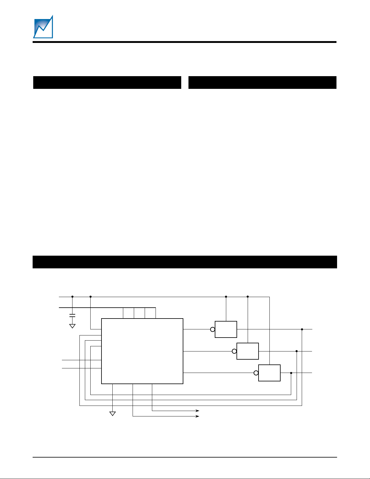
SIMPLIFIED APPLICATION DRAWING
5V
2
I
C
0.01µF
Reset#
16
14
15
7
A2
V
0
2
V
1
3
V
2
V
3
1
MR#
WLDI
GND
RESET#
8
9
6
SDA
A1
SMS44
IRQ#
11
10
SCL
PUP#1
PUP#2
PUP#3
12
4
5
13
LDO
LDO
LDO
3.3V
2.5V
1.8V
2047 SAD 2.0
Closed Loop Power-up Supply Cascading
©SUMMIT MICROELECTRONICS, Inc., 2001 • 300 Orchard City Dr., Suite 131 • Campbell, CA 95008 • Phone 408-378-6461 • FAX 408-378-6586 • www.summitmicro.com
Characteristics subject to change without notice 2047 4.0 6/7/01
1
Page 2
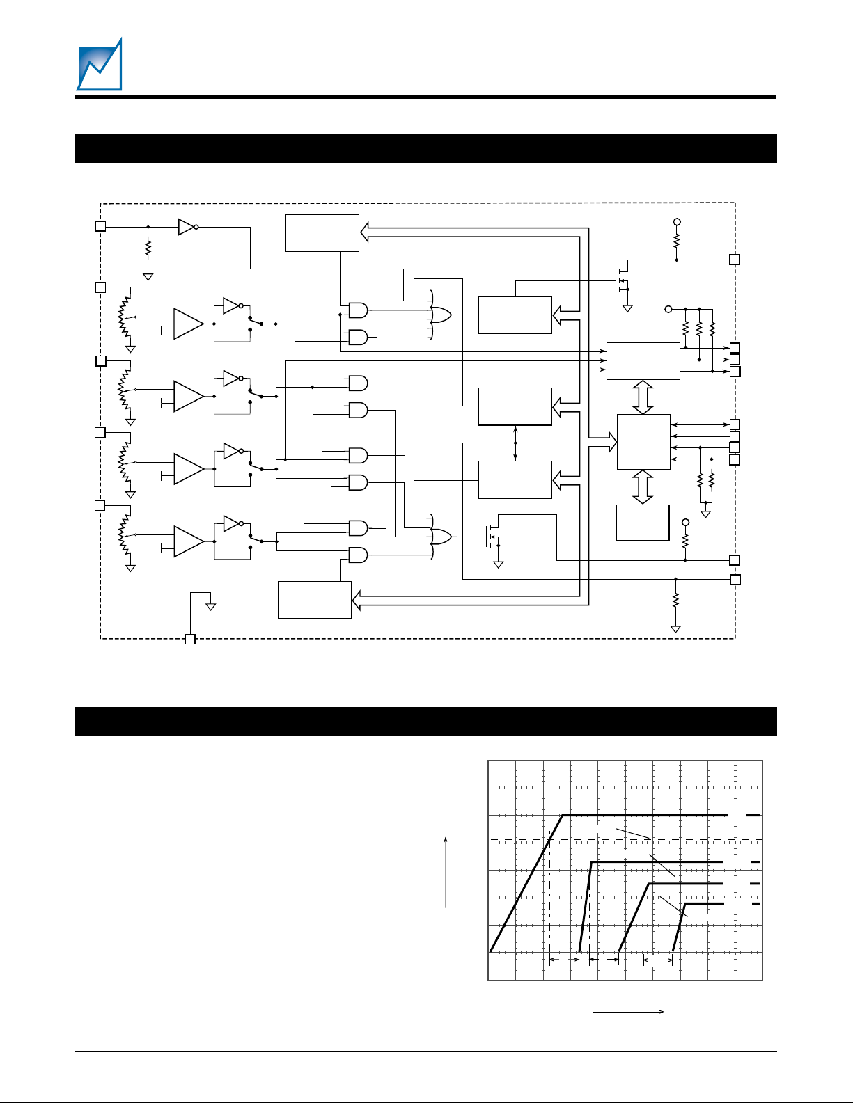
FUNCTIONAL BLOCK DIAGRAM
MR#
1
70kΩ
V
16
0
NV DAC
+
–
REF
V
2
1
NV DAC
+
–
REF
V
3
2
NV DAC
+
–
REF
V
14
3
NV DAC
+
–
REF
RESET
IRQ
RESET
IRQ
RESET
IRQ
RESET
IRQ
CONFIGURATION
REGISTER
CONFIGURATION
REGISTER
PROGRAMMABLE
RESET PULSE
GENERATOR
PROGRAMMABLE
LONGDOG
TIMER
PROGRAMMABLE
WATCHDOG
TIMER
V
CC
70kΩ
PROGRAMMABLE
POWER
CASCADING
SERIAL
BUS
CONTROL
LOGIC
4K-BIT NV
MEMORY
SMS44
Preliminary
V
CC
70kΩ
11
70kΩ
70kΩ
4
5
13
9
10
7
6
70kΩ70kΩ
V
CC
70kΩ
12
15
70kΩ
RESET#
PUP#1
PUP#2
PUP#3
SDA
SCL
A2
A1
IRQ#
WLDI
8
GND
CASCADING
If a specific order in which the supplies are turned on and
brought up to their valid voltage levels is needed, time
based sequencing will not suffice. In this case supply
cascading should be utilized, where the supplies are
enabled a certain period of time after the previous voltage
has reached its minimum valid level. Figure 1 shows that
each succeeding voltage must reach its minimum valid
level before the timer is started to time the interval, t, for
the next voltage. The duration of each t is programmable.
The next supply is not enabled until the timer has elapsed.
See also Figure 5.
2047 BD 4.0
6V
5V
5V Valid
4V
V
2V
0V
t
3.3V Valid
t
3.3V
2.5V
1.8V
2.5V Valid
t
T
2047 Fig01
Figure 1. Cascading Power Supplies
2
2047 4.0 6/7/01
SUMMIT MICROELECTRONICS, Inc.
Page 3
PIN CONFIGURATION PIN NAMES
SMS44
Preliminary
MR#
V
V
PUP#1
PUP#2
A1
A2
GND
16-Pin SOIC or
16-Pin SSOP
1
2
1
3
2
4
5
6
7
8
16
15
14
13
12
11
10
9
2047 PCon 2.0
V
0
WLDI
V
3
PUP#3
IRQ#
RESET#
SCL
SDA
niPemaNnoitcnuF
1#RMtupniteserlaunaM
2V
3V
1
2
41#PUPtuptuodettimreppurewoP
52#PUPtuptuodettimreppurewoP
61AtupnisserddA
72AtupnisserddA
8DNGnruterylppusrewoP
9ADSO/IatadlaireS
01LCSkcolcatadlaireS
11#TESERtuoteseR
21#QRItuotpurretnI
313#PUPtuptuodettimreppurewoP
41V
51IDLW
61V
3
tpurretni
0
tupnirotinomdnaylppusegatloV
tupnirotinomdnaylppusegatloV
tupnirotinomdnaylppusegatloV
remitgodgnol/godhctaW
tupnirotinomdnaylppusegatloV
2047 Pins Table 2.0
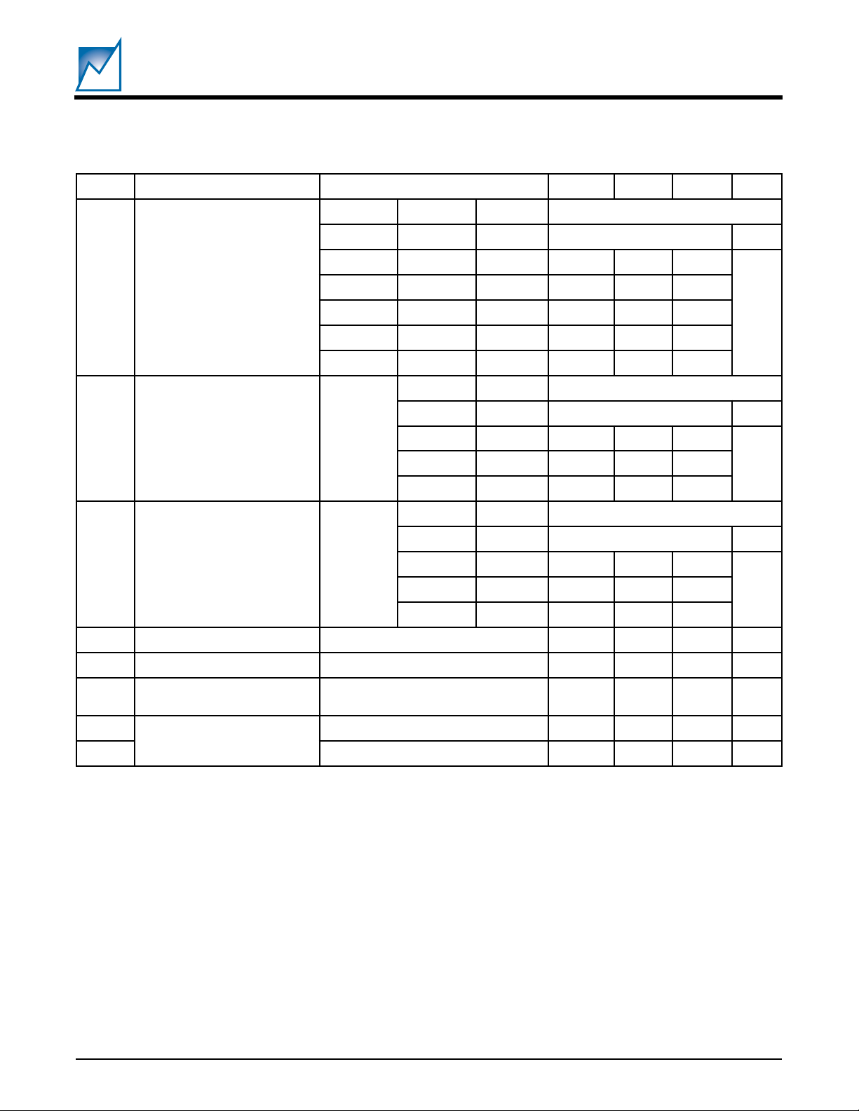
RECOMMENDED OPERATING CONDITIONS
Temperature –40ºC to 85ºC.
Voltage 2.7V to 5.5V
SUMMIT MICROELECTRONICS, Inc.
2047 4.0 6/7/01
3
Page 4
ABSOLUTE MAXIMUM RATINGS*
SMS44
Preliminary
Temperature Under Bias ......................–55°C to 125°C
Storage Temperature ...........................–65°C to 150°C
Lead Solder Temperature (10s) .........................300 °C
Terminal Voltage with Respect to GND:
V0, V1, V2, and V3.......... –0.3V to 6.0V
All Others ...................... –0.3V to 6.0V
*COMMENT
Stresses beyond the listed Absolute Maximum Ratings may cause
permanent damage to the device. These are stress ratings only, and
functional operation of the device at these or any other conditions
outside those listed in the operational sections of this specification is not
implied. Exposure to any absolute maximum rating for extended
periods may affect device performance and reliability.
DC OPERATING CHARACTERISTICS
(Over Recommended Operating Conditions; Voltages are relative to GND)
lobmySretemaraPsetoN.niM.pyT.xaMtinU
-tuoteserdilavaotsrefer.nimV1
detareneggniebtup
V
CC
I
CC
V
HTP
egnaR
V
HTP
V
TSYH
V
LO
egnar
V
TSR
tnerrucylppuS
siseretsyh 03Vm
egatlovylppusgnitarepO
ta:snoitarepoetirw/daeryromeM
taebtsumstupniVehtfoenotsael
Vevobaro
≤ V;V5.5
V
CC
V
3
.nim
CC
V;V7.4tnioppirt
0
V=#RM;DNG=
CC
1V,2
stuptuolla;
,
gnitaolf
yromemroretsigernoitarugifnoC
ssecca
dlohserhtelbammargorP
V
3
)stnemercniVm02(
VegnaregatlovdlohserhtteseR
ot
0
dlohserhtelbammargorP5.2– V
V,Am2.1=
I
tuptuoegatlovwoL
KNIS
I
KNIS
≥ V7.23.0V
CC
V,Aµ002=
CC
V2.1=3.0V
1OTR0OTR
0.15.5V
7.25.5V
002004Aµ
3Am
9.00.6V
HTP
5.2%
00025203sm
t
OTRP
htdiw
eslupteserelbammargorP
01530556sm
1056001531sm
11031002072sm
t
TSRD
4
yaled#TESERotniVevirdrevoVm00102sµ
2047 Elect TableA 4.2
2047 4.0 6/7/01
SUMMIT MICROELECTRONICS, Inc.
Page 5
lobmySretemaraPsetoN.niM.pyT.xaMtinU
2DW1DW0DW
000 FFO —
011 004
t
OTDWP
doirepremit
godhctaWelbammargorP
100 008
101 0061
110 0023
111 0046
1DL0DL
00 FFO —
t
OTDLP
doirepremit
godgnoLelbammargorP
01 0061
11 0046
SMS44
Preliminary
sm
sm10 0023
1-X#PUP0-X#PUP
00 FFO —
t
X
YLDP
V
HTP
tuo#PUPot
morfyaledelbammargorP
01 52
sm10 05
11 001
I
RM
T
RM
T
TSRRMD
V
LI
V
HI
wol#TESER
tnerrucpullup#RM 001Aµ
htdiwesluptupni#RM 003sn
otwol#RMmorfyaleD
002sn
dlohserhttupnI
7.0 × V
CC
6.0V
V
2047 Elect TableB 4.2
SUMMIT MICROELECTRONICS, Inc.
2047 4.0 6/7/01
5
Page 6
PIN DESCRIPTIONS
SMS44
Preliminary
V0, V1, V2, V3 (16, 2, 3, 14)
These inputs are used as the voltage monitor inputs and
as the voltage supply for the SMS44. Internally they are
diode ORed and the input with the highest voltage
potential will be the default supply voltage.
The RESET# output will be true if any one of the four inputs
is above 1V. However, for full device operation at least
one of the inputs must be at 2.7V or higher.
The sensing threshold for each input is independently
programmable in 20mV increments from 0.9V to 6.0V.
Also, the occurrence of an under- or over-voltage condition that is detected as a result of the threshold setting can
be used to generate subsequent action(s), such as
RESET# or IRQ#. The programmable nature of the
threshold voltage eliminates the need for external voltage
divider networks.
GND
Power supply return.
MR# (1)
The manual reset input always generates a RESET#
output whenever it is driven low. The duration of the
RESET# output pulse will be initiated when MR# goes low
and it will stay low for the duration of MR# low plus the
programmed reset time-out period (t
). If MR# is
PRTO
brought low during a power-on cascade of the PUP#s the
cascade will be halted for the reset duration, and will then
resume from the point at which it was interrupted. MR#
must be held low during a configuration register Write or
Read. This signal is pulled down internally through a 70kΩ
resistor, consequently the part is normally in reset mode
when powered down.
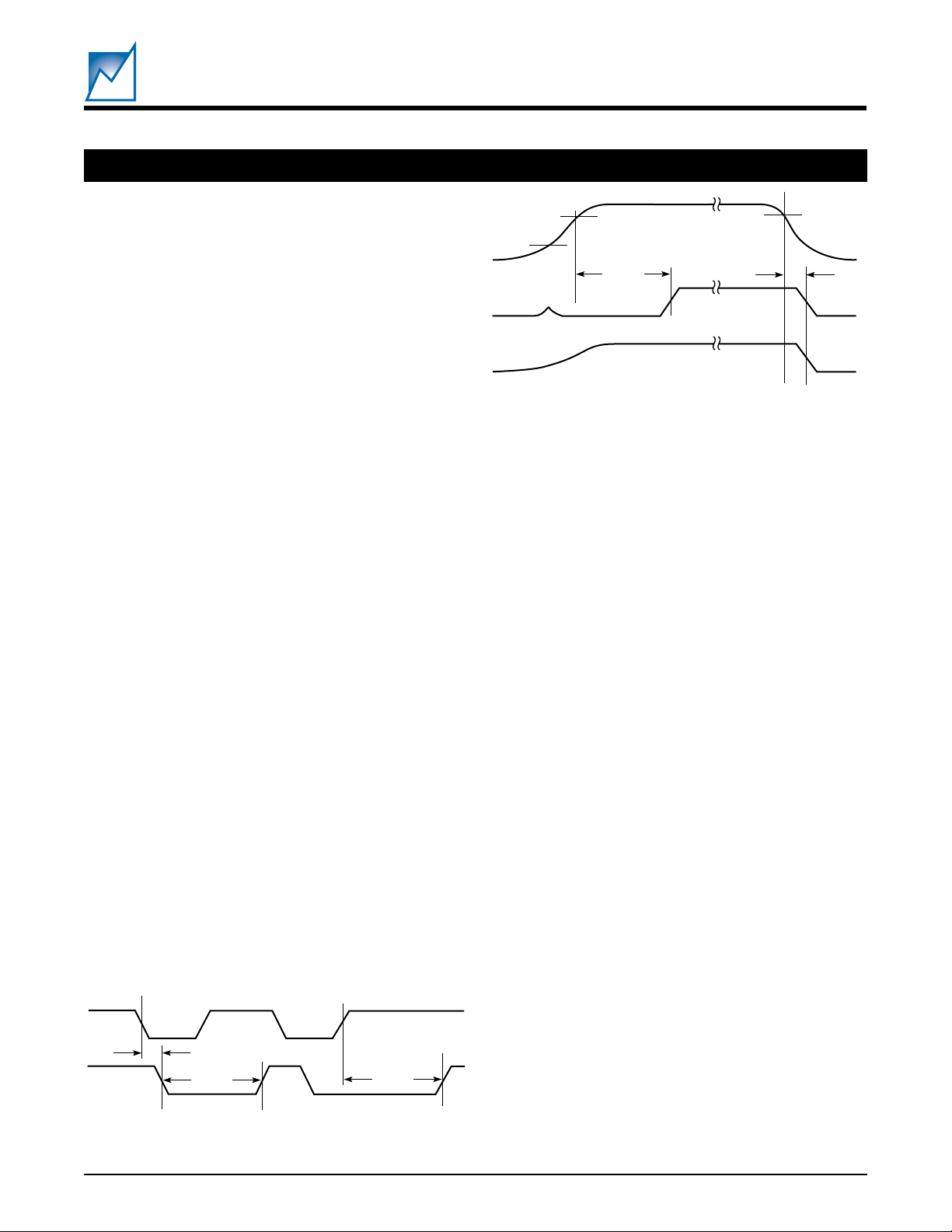
RESET# (11)
The reset output is an active low open drain output. It will
be driven low whenever the MR# input is low or whenever
an enabled under-voltage or over-voltage condition ex-
MR#
t
DMRRST
RESET#
t
PRTO
t
PRTO
V
RST
2047 Fig03 2.0
V0 — V
RESET#
IRQ#
V
3
PTH
t
PRTO
t
D
Figure 3. RESET# Timing with IRQ#
ists, or when a longdog timer expiration exists. The four
voltage monitor inputs are always functioning, but their
ability to generate a reset is programmable (configura-
tion register 4). Refer to Figures 2 and 3 for a detailed
illustration of the relationship between MR#, IRQ#, RESET# and the VIN levels. This signal is pulled up internally
through a 70kΩ resistor.
IRQ# (12)
The interrupt output is an active low open-drain output. It
will be driven low whenever the watchdog timer times out
or whenever an enabled under-voltage or over-voltage
condition on a V input exists (configuration register 6).
This signal is pulled up internally through a 70kΩ resistor.
WLDI (15)
Watchdog and longdog timer interrupt input. A low to high
transition on the WLDI input will clear both the watchdog
and longdog timers, effectively starting a new time-out
period. This signal is pulled down internally through a
70kΩ resistor.
If WLDI is stuck low and no low-to-high transition is
received within the programmed t
PWDTO
period (programmed watch dog time-out) IRQ# will be driven low. If
a transition is still not received within the programmed
t
period (programmed longdog time-out) RESET#
PLDTO
will be driven low. Refer to Figure 4 for a detailed
illustration.
Holding WLDI high will block interrupts from occurring but
will not block the longdog from timing out and generating
a reset. Refer to Figure 4 for a detailed illustration of the
relationship between IRQ#, RESET#, and WLDI.
2047 Fig02 2.0
Figure 2. RESET# Timing with MR#
6
2047 4.0 6/7/01
SUMMIT MICROELECTRONICS, Inc.
Page 7

SMS44
Preliminary
A1, A2 (6, 7)
A1 and A2 are the address inputs. When addressing the
SMS44 memory or configuration registers the address
inputs distinguish which one of four possible devices
sharing the common bus is being addressed. These
signals are pulled down internally through 70kΩ resistors.
SDA (9)
SDA is the serial data input/output pin. It should be tied
to V
through a pull-up resistor.
CC
SCL (10)
SCL is the serial clock input. It should be tied to V
CC
through a pull-up resistor.
t
PWDTO
t
t
0
IRQ#
RESET#
t
PLDTO
WLDI
t
0
t
PRTO
t
0
t
0
0
t
PRTO
t
PLDTO
2047 Fig04 3.0
PUP#1, PUP#2, PUP#3 (4, 5, 13)
These are the power-up permitted outputs when the
SMS44 is programmed to provide the cascading of LDOs
or DC/DC converters (
tions of cascading
see Figures 1 and 5 for illustra-
). Each delay is independently
enabled and programmable for its duration (configura-
tion register 7). If all PUP# outputs are enabled the order
of events would be as follows: V0 above threshold then
delay to PUP#1 turning on; V
above threshold then delay
1
to PUP#2 turning on; V2 above threshold then delay to
PUP#3 turning on. The delays are programmable. These
signals are pulled up internally through 70kΩ resistors.
Figure 4. Watchdog, Longdog and WLDI Timing
SUMMIT MICROELECTRONICS, Inc.
2047 4.0 6/7/01
7
Page 8

DEVICE OPERATION
SMS44
Preliminary
SUPPLY AND MONITOR FUNCTIONS
The V0, V1, V2, and V3 inputs are internally diode-ORed so
that any one of the four can act as the device supply. The
RESET# output will be guaranteed true so long as one of
the four pins is at or above 1V.
Note
: for performing a memory operation (Read
or Write) and to have the ability to change
configuration register contents at least one supply input must be above 2.7V.
Read/Write operations require a 0.01µF capacitor from
the highest Vx input (normally V0) to GND. For optimum
performance connect capacitors from each of the Vx
If cascading is enabled, the designer must insure V
primary supply and is the first to become active.
Associated with each input is a comparator with a programmable threshold for detection of under-voltage conditions on any of the four supply inputs. The threshold can
be programmed in 20mV increments anywhere within the
range of 0.9V to 6.0V. Configuration registers 0, 1, 2, and
3 adjust the thresholds for V0, V1, V2, and V3 respectively.
If the value contained in any register is all zeroes, the
corresponding threshold will be 0.9V. If the contents were
05
the threshold would then be 1.0V [0.9V + (5 ×
HEX
0.02V)]. All four registers are configured as 8-Bit registers.
inputs to GND. Locate the capacitors as physically close
to the SMS44 as possible.
7D
BSM
6D5D4D3D2D1D
0D
BSL
11111111 V0.6=tnemtsujdadlohserhttsehgiH
00000000 V0.6=tnemtsujdadlohserhttsewoL
00000110 6(+V9.0=dlohserhT × V20.1=)V20.0
Table 1. Configuration Registers 0, 1, 2, and 3
is the
0
noitcA
).g.e(
2047 Table01
RESET AND IRQ FUNCTIONS
Both the reset and interrupt outputs have four programmable sources for activation. Configuration register 4 is
used for selecting the activation source, which can be any
combination of V0, V1, V2 and V3. A monitor input can only
be programmed to activate on either an under-voltage or
over-voltage condition, but not both conditions.
The RESET# output will become active when triggered by
a selected activation source such as an under-voltage
condition on V1. When this condition ceases, the RESET# output will remain active for t
reset time-out). This reset time-out interval takes priority
over the PUP outputs for use of the timer.
7D
V
3
6D5D4D3D2D1D
BSM
V
V
2
V
1
V
0
3
ecruoSreggirTTESERecruoSreggirTQRI
Table 2. Configuration Register 4
(programmable
PRTO
V
2
V
1
2047 Table02
0D
BSL
V
0
The RESET# output has two hardwired sources for
activation: the MR# input, and the expiration of the
Longdog timer. RESET# will remain active so long as
MR# is low, and will continue driving the RESET# output
for t
(programmable reset time out) after MR# returns
PRTO
high. The MR# input cannot be bypassed or disabled. The
Longdog timer can be bypassed by programming it to the
off or idle mode.
The sole hardwired source for driving the IRQ# output low
is the watchdog. The IRQ# circuitry is disabled during
initial power up until the reset condition has terminated
and the reset interval (t
) has timed out. The IRQ#
PRTO
output is cleared by a low-to-high transition of the WLDI
signal. It can effectively be bypassed by programming it
to the off or idle mode. Refer to Figures 2, 3 and 4 for a
detailed illustration of the relationships among the affected signals.
The SMS44 also provides the option of the monitors
triggering on either an under-voltage or over-voltage
condition. The low-order four bits of configuration register
5 program these options.
8
2047 4.0 6/7/01
SUMMIT MICROELECTRONICS, Inc.
Page 9

SMS44
Preliminary
3D
noitcA
V
3
2D1D
BSM
V
V
2
0D
BSL
V
1
0
selbane0agnitirW
rofnoitcetedegatlovrednu
0000
tupniVdetceleseht
selbane1agnitirW
rofnoitcetedegatlovrevo
1111
tupniVdetceleseht
2047 Table03
Table 3. Configuration Register 5 (D0 through D3)
The high order four bits of configuration register 5 are
Read only, and their state indicates the sources of
interrupts. Whenever an interrupt is generated the status
of the V inputs will be recorded in the status register. The
status will remain in the register until the device is
powered-down or another interrupt occurs that overwrites
the previous status.
If an interrupt occurs and no bits are set the default
assumption must be the watchdog generated the interrupt.
7D
V
3
6D5D
BSM
V
V
2
0000
1111
4D
BSL
V
1
0
noitcA
ehtsetacidni1agnidaeR
tpurretniehtfoecruos
2047 Table04
Table 4. Configuration Register 5 (D4 through D7)
WATCHDOG AND LONGDOG TIMERS
The SMS44 contains two timers that can be programmed
independently. The Watchdog is intended to be of shorter
duration and will generate an interrupt if it times out. The
Longdog timer will generally be programmed to be of
longer duration than the watchdog and it will generate a
reset if it times out. Both timers are cleared by a low to high
transition on WLDI and they both start simultaneously.
If the watchdog should time-out the device status will be
recorded in the status register. If the Longdog times out
RESET# will be driven low either until a WLDI clear is
received or until t
time it will return high. Refer to Figure 4 which illustrates
the action of RESET# and IRQ# with respect to the
Watchdog and Longdog timers and the WLDI input.
(whichever occurs first), at which
PRTO
7D
BSM
6D5D4D3D
SAC1OTR0OTR1DL0DLnoitcA
xxx
xxx
xxx
xxx
x
x
x
x
0
1
00
01
10
11
xxxx nOedacsaC
xxxx ffOedacsaC
00
01
10
11
xxt
xxt
xxt
xxt
OTRP
OTRP
OTRP
OTRP
2047 Table05
ffOgodgnoL
sm0061
sm0023
sm0046
sm52=
sm05=
sm001=
sm002=
Table 5. Configuration Register 6 (D3 through D7)
2D1D
0D
BSL
noitcA2DW1DW0DW
FFO 000
sm004011
sm008100
sm0061101
sm0023110
sm0046 111
2047 Table06 1.0
Table 6. Configuration Register 6 (D0, D1, D2)
If WLDI is held low the timers will free-run generating a
series of interrupts and resets. If WLDI is held high the
interrupt (watchdog) output will be disabled and only the
reset (Longdog) output will be active.
When the Longdog times out RESET# will be generated.
When RESET# returns high (after t
or after a WLDI
PRTO
strobe) both timers are reset to time zero. Therefore, if
the Longdog t
watchdog t
PWDTO
is equal to or shorter than the
PLDTO
, RESET# will effectively clear the
interrupt before it can drive the output low.
Register 6 is also used to set the programmable reset
time-out period (t
) and to select the cascade option.
PRTO
SUMMIT MICROELECTRONICS, Inc.
2047 4.0 6/7/01
9
Page 10

SMS44
Preliminary
Cascade Delay Programming
The cascade delays are programmed in register 7. Bit 7
of register 6 must be set to a 0 in order to enable the
cascading of the PUP# outputs. Cascading will not
commence until V0 is above its programmed threshold.
Each PUP# (-3, -2 and -1) is delayed according to the
states of its Bit 1 and Bit 0 as indicated in Table 9. Refer
to Figures 1 and 5 for the detailed timing relationship of
the programmable power-on cascading.
The delay from V
a similar t
PDLYX
until PUP#1 low is t
PTH0
PDLY1
. There is
delay for V1 to PUP#2 and V2 to PUP#3.
They are programmed in register 7. Cascading will
always occur as indicated in the flow chart (Figure 7).
7D
6D
BSM
sserddA
tceleS
noitcA
kcoL0SA
x
x
0
1
0
1
xdelbaneetirW/daeR.geR.gifnoC
xtuodekcoletirW/daeR.geR.gifnoC
nehwylnosdnopser,0101=ITD
setatscigol1A&2A=stibsserdda
nehwylnosdnopser,1101=ITD
setatscigol1A&2A=stibsserdda
2047 Table07 3.0
Table 7. Configuration Register 7 (D7, D6)
5D4D3D2D1D
0D
BSL
3#PUP2#PUP1#PUP
1tiB0tiB1tiB0tiB1tiB0tiB
2047 Table08 3.0
Table 8. Configuration Register 7 (D5 through D0)
1tiB0tiBt
XYLDP
00 yaleD)on(sm0
01 yaleDsm52
10 yaleDsm05
11 yaleDsm001
2047 Table09 1.0
Table 9. PUP Delays, Configuration Register 7
10
2047 4.0 6/7/01
SUMMIT MICROELECTRONICS, Inc.
Page 11

V
0
RESET#
PUP1#
V
1
PUP2#
V
2
PUP3#
V
PTH0
t
PDLY1
V
PTH1
t
PDLY2
V
PTH2
t
PDLY3
t
PRTO
SMS44
Preliminary
V
3
Figure 5. VX Input and Resulting PUP# Cascade (RESET# set to trip on V3 Undervoltage)
V
V0
PUP1#
V1
PUP2#
V2
PTH0
50ms
V
50ms
2047 Fig05
PTH2
SUMMIT MICROELECTRONICS, Inc.
PUP3#
Figure 6. Timing with Register 7 Contents 22
2047 4.0 6/7/01
2047 Fig06
HEX
11
Page 12

HOOKUP
SMS44
Preliminary
Cascading
Enabled
V
0
>V
?
PTH
Yes
t
PDLY1
Turn On PUP#1
V1
?
>V
PTH
Yes
t
PDLY2
Turn On PUP#2
V2
?
>V
PTH
Yes
t
PDLY3
No
No
No
HARDWARE
The end user can use the summit SMX3200 programming
cable and software that have been developed to operate
with a standard personal computer. The programming
cable interfaces directly between a PC’s parallel port and
the target application. The application’s values are
entered via an intuitive graphical user interface employing
drop-down menus. See also Figure 13.
After the desired settings for the application are determined the software will generate a hex file that can be
transferred to the target device or downloaded to Summit.
If it is downloaded to Summit a customer part number will
be assigned and the file will be used to customize the
devices during the final electrical test operations.
Top view of straight 0.1" × 0.1" closed
side connector SMX3200 interface
Positive Supply
Negative Supply
Pin 10, Reserved
Pin 8, Reserved
Pin 6, MR#
Pin 4, SDA
Pin 2, SCL
V
SMS44
GND
0
A1
A2
MR#
SDA
SCL
10
9
8
7
6
5
4
3
2
1
Figure 8. Programming Hookup
Pin 9, 5V
Pin 7, 10V
Pin 5, Reserved
Pin 3, GND
Pin 1, GND
C1
0.01µF
2047 Fig08
12
Turn On PUP#3
2047 Fig07
Figure 7. Cascade Flow Chart
2047 4.0 6/7/01
SUMMIT MICROELECTRONICS, Inc.
Page 13

INTERFACE
SMS44
Preliminary
MEMORY OPERATION
Data for the configuration registers and the memory array
are read and written via an industry standard two-wire
interface. The bus was designed for two-way, two-line
serial communication between different integrated circuits. The two lines are a serial data line (SDA) and a
serial clock line (SCL). The SDA line must be connected
to a positive supply by a pull-up resistor, located somewhere on the bus. See Memory Operating Characteristics: Table 10 and Figure 9.
Input Data Protocol
The protocol defines any device that sends data onto the
bus as a transmitter and any device that receives data as
a receiver. The device controlling data transmission is
called the Master and the controlled device is called the
Slave. In all cases the SMS44 will be a Slave device,
since it never initiates any data transfers.
One data bit is transferred during each clock pulse. The
data on the SDA line must remain stable during clock high
time because changes on the data line while SCL is high
will be interpreted as start or stop condition.
lobmySretemaraPsnoitidnoC.niM.xaMstinU
f
LCS
t
WOL
t
HGIH
t
FUB
t
ATS:US
t
ATS:DH
t
OTS:US
t
AA
t
HD
t
R
t
F
t
TAD:US
t
TAD:DH
ycneuqerfkcolcLCS 0001zHk
doirepwolkcolC 7.4sµ
doirephgihkcolC 0.4sµ
)1(emiteerfsuBnoissimsnartwenerofeB7.4sµ
emitputesnoitidnoctratS 7.4sµ
emitdlohnoitidnoctratS 0.4sµ
emitputesnoitidnocpotS 7.4sµ
)1(tuptuodilavotegdekcolC)nelcyc(ADSdilavotwolLCS3.05.3sµ
)1(emitdlohtuOataDegnahcADSot)1+nelcyc(wolLCS3.0sµ
)1(emitesirADSdnaLCS 0001sn
)1(emitllafADSdnaLCS 003sn
)1(emitputesnIataD 052sn
)1(emitdlohnIataD 0sn
IT)1(ADSdnaLCSretlifesioNnoisserppusesioN001sn
t
RW
Note (1): These values are guaranteed by design.
emitelcycetirW 5sm
Table 10. Memory Operating Characteristics
t
R
SCL
t
SU:STA
SDA In
t
SDA Out
Figure 9. Memory Operating Characteristics
SUMMIT MICROELECTRONICS, Inc.
2047 Table10 4.0
t
HIGH
t
F
t
HD:STA
AA
t
HD:DAT
t
LOW
t
DH
2047 4.0 6/7/01
t
SU:DAT
t
SU:STO
t
BUF
2047 Fig09
13
Page 14

SMS44
Preliminary
START and STOP Conditions
When both the data and clock lines are high the bus is said
to be not busy. A high-to-low transition on the data line,
while the clock is high, is defined as the Start condition.
A low-to-high transition on the data line, while the clock
is high, is defined as the Stop condition. See Figure 10.
START
Condition
SCL
SDA In
STOP
Condition
2047 Fig10
Figure 10. START and STOP Conditions
Acknowledge (ACK)
Acknowledge is a software convention used to indicate
successful data transfers. The transmitting device,
either the Master or the Slave, will release the bus after
transmitting eight bits. During the ninth clock cycle the
receiver will pull the SDA line low to Acknowledge that it
received the eight bits of data. The Master will leave the
SDA line high (NACK) when it terminates a read function.
The SMS44 will respond with an Acknowledge after
recognition of a Start condition and its slave address byte.
If both the device and a write operation are selected the
SMS44 will respond with an Acknowledge after the receipt
of each subsequent 8-Bit word. In the READ mode the
SMS44 transmits eight bits of data, then releases the SDA
line, and monitors the line for an Acknowledge signal. If
an Acknowledge is detected and no Stop condition is
generated by the Master, the SMS44 will continue to
transmit data. If a NACK is detected the SMS44 will
terminate further data transmissions and await a Stop
condition before returning to the standby power mode.
Device Addressing
Following a Start condition the Master must output the
address of the Slave it is accessing. The most significant
four bits of the Slave address are the device type
identifier/address. For the SMS44 the default is 1010
BIN
The next two bits are the Bus Address. The next bit (the
7th) is the MSB of the memory address.
7D
6D5D4D3D2D1D
BSM
stiBsserddA
epyTeciveDsuBBSMW/R
44SMSxxxx
1001
10 10
10 11
! retsigeRnoitarugifnoC
! )tluafed(yromeM
! yromeMetanretlA
2047 Table11 1.0
Table 11. Slave Addresses
Read/Write Bit
The last bit of the data stream defines the operation to be
performed. When set to 1 a Read operation is selected;
when set to 0 a Write operation is selected.
WRITE OPERATIONS
The SMS44 allows two types of Write operations: byte
Write and page Write. A byte Write operation writes a
single byte during the nonvolatile write period (tWR). The
page Write operation, limited to the memory array, allows
up to 16 bytes in the same page to be written during tWR.
Byte Write
After the Slave address is sent (to identify the Slave
device and select either a Read or Write operation), a
second byte is transmitted which contains the low order
8 bit address of any one of the 512 words in the array.
Upon receipt of the word address the SMS44 responds
with an Acknowledge. After receiving the next byte of data
it again responds with an Acknowledge. The Master then
terminates the transfer by generating a Stop condition, at
which time the SMS44 begins the internal Write cycle.
While the internal Write cycle is in progress the SMS44
inputs are disabled and the device will not respond to any
requests from the Master.
Page Write (memory only)
The SMS44 is capable of a 16-byte page Write operation.
It is initiated in the same manner as the byte Write
operation, but instead of terminating the Write cycle after
the first data word the Master can transmit up to 15 more
bytes of data. After the receipt of each byte the SMS44
will respond with an Acknowledge.
.
The SMS44 automatically increments the address for
subsequent data words. After the receipt of each word the
low order address bits are internally incremented by one.
0D
BSL
14
2047 4.0 6/7/01
SUMMIT MICROELECTRONICS, Inc.
Page 15

SMS44
Preliminary
The high order bits of the address byte remain constant.
Should the Master transmit more than 16 bytes, prior to
generating the Stop condition, the address counter will
rollover and the previously written data will be overwrit-
Master
SDA
Slave
Master
SDA
Slave
S
T
A
Device T ype
R
Address
T
S
T
Typical Reading Operation
A
(Alternate memory device type)
R
T
10
11
Bus
Address
B
A
0110
2
B
A
2
B
A
A
8
1
B
A
A
8
1
Typical Write Operation
(Standard memory device type)
R
A7A6A5A4A3A2A1A
/
W
A
C
K
R
A7A6A5A4A3A2A1A
/
W
A
C
K
0
ten. As with the byte Write operation, all inputs are
disabled during the internal Write cycle. Refer to Figure
11 for the address, Acknowledge, and data transfer
sequence.
S
T
O
P
D7D6D5D4D3D2D1D
0
A
C
K
S
T
A
A
C
R
K
T
10
11
0
A
C
K
B
B
R
A
A
A
8
2
1
D7D6D5D4D3D2D1D
/
W
A
C
K
Up to 15
additional bytes
can be written
before issuing
the stop.
N
A
C
K
0
S
T
O
P
S
T
Master
SDA
A
R
T
10
01
Slave
S
T
A
Master
SDA
Reading the Configuration Register
R
T
01
10
Slave
SUMMIT MICROELECTRONICS, Inc.
Writing Configuration Registers
B
A
2
B
A
2
R
B
X
A
1
B
X
A
1
C7C6C5C4C3C2C1C
/
W
A
C
K
R
C7C6C5C4C3C2C1C
/
W
A
C
K
Figure 11. Read and Write Operations
2047 4.0 6/7/01
D7D6D5D4D3D2D1D
0
A
C
K
S
T
A
A
C
R
K
T
0
10
01
S
T
O
P
0
A
C
K
N
S
A
T
C
O
K
P
B
B
R
A
A
X
2
1
D7D6D5D4D3D2D1D
/
W
A
C
K
0
2047 Fig11
15
Page 16

SMS44
Preliminary
Acknowledge Polling
When the SMS44 is performing an internal Write operation it will ignore any new Start conditions. Since the
device will only return an acknowledge after it accepts the
Start the part can be continuously queried until an
acknowledge is issued, indicating that the internal Write
cycle is complete. See the flow chart for the proper
sequence of operations for polling.
Write Cycle
In Progress
Issue Start
Issue Stop
Issue Slave
Address and
R/W = 0
No
No
Issue Stop
Await
Next
Command
2047 Fig12
ACK
Returned
Yes
Next
Operation
a Write?
Yes
Issue
Address
Proceed
With
Write
Figure 12. Write Flow Chart
READ OPERATIONS
Read operations are initiated with the R/W bit of the
identification field set to 1. There are two different Read
options: 1. Current Address Byte Read, and 2. Random
Address Byte Read.
Current Address Read (memory only)
The SMS44 contains an internal address counter which
maintains the address of the last word accessed, incremented by one. If the last address accessed (either a
Read or Write) was to address location n, the next Read
operation would access data from address location n+1
and increment the current address pointer. When the
SMS44 receives the Slave address field with the R/W bit
set to 1 it issues an acknowledge and transmits the 8-Bit
word stored at address location n+1. The current address
byte Read operation only accesses a single byte of data.
The Master sets the SDA line to NACK and generates a
stop condition. At this point the SMS44 discontinues data
transmission.
Random Address Read (Register and Memory)
Random address Read operations allow the Master to
access any memory location in a random fashion. This
operation involves a two-step process. First, the Master
issues a write command which includes the start condition and the Slave address field (with the R/W bit set to
Write), followed by the address of the word it is to Read.
This procedure sets the internal address counter of the
SMS44 to the desired address. After the word address
acknowledge is received by the Master it immediately
reissues a Start condition, followed by another Slave
address field with the R/W bit set to READ. The SMS44
will respond with an Acknowledge and then transmit the
8 data bits stored at the addressed location. At this point
the Master sets the SDA line to NACK and generates a
Stop condition. The SMS44 discontinues data transmission and reverts to its standby power mode.
Sequential READ (Memory Only)
Sequential Reads can be initiated as either a current
address Read or random access Read. The first word is
transmitted as with the other byte Read modes (current
address byte Read or random address byte Read);
however, the Master now responds with an Acknowledge,
indicating that it requires additional data from the SMS44.
The SMS44 continues to output data for each Acknowledge received. The Master terminates the sequential
Read operation by responding with a NACK, and issues
a Stop condition. During a sequential Read operation the
internal address counter is automatically incremented
with each Acknowledge signal. For Read operations all
address bits are incremented, allowing the entire array to
be read using a single Read command. After a count of
the last memory address the address counter will rollover
and the memory will continue to output data.
16
2047 4.0 6/7/01
SUMMIT MICROELECTRONICS, Inc.
Page 17

V0
V1
V2
V3
C2
C3
NOTES:
1. C1, C2, C3 and C4 are all 0.01µF.
APPLICATIONS
R1
10kΩ
C4
2
1
4
3
6
5
J1
8
7
10
9
Figure 13. Application Schematic
C1
16
14
10
1
2
3
9
6
7
MR#
V0
V1
V2
V3
SMS44
SCL
SDA
A1
A2
RESET#
GND
PUP#1
PUP#2
PUP#3
IRQ#
WLDI
8
SMS44
Preliminary
4
5
13
11
12
15
2047 Fig13
2. C1 is required for Read/Write operations.
3. C2, C3, and C4 are recommended for noisy environments and whenever input voltages are near the OV
and/or UV reset level trip points.
4. Connector J1 is an SMX3200 (see Figure 8).
5. The signal MR# has an internal pull-down resistor.
Resistor R1 is required to provide pull-up.
SUMMIT MICROELECTRONICS, Inc.
2047 4.0 6/7/01
17
Page 18

ORDERING INFORMATION
SMS44
Preliminary
Base Part Number
PACKAGES
16 PIN SOIC PACKAGE
SMS44
G
Package
G = SSOP
S = SOIC
2047 Tree 1.0
0.386 - 0.394
(9.80 - 10.00)
0.0075 - 0.01
(0.19 - 0.25)
Ref. JEDEC MS-012
Inches
(Millimeters)
0.150 - 0.157
(3.80 - 4.00)
0.01 - 0.02
(0.25 - 0.50)
0.016 - 0.050
0.016 - 0.050
×45º
(0.40 - 1.27)
0 to 8
typ
0.053 - 0.069
(1.35 - 1.75)
0.05
(1.27)
0.228 - 0.244
(5.80 - 6.20)
1
0.004 - 0.01
0.013 - 0.020
(0.33 - 0.51)
(0.10 - 0.25)
16 Pin SOIC
18
2047 4.0 6/7/01
SUMMIT MICROELECTRONICS, Inc.
Page 19

Ref. JEDEC MO-137
SMS44
Preliminary
16 PIN SSOP PACKAGE
0.189 - 0.197
(4.80 - 5.00)
0.228 - 0.244
(5.79 - 6.20)
Inches
(Millimeters)
0.150 - 0.157
(3.81 - 3.99)
0.053 - 0.069
(1.35 - 1.75)
0.007 - 0.010
(0.18 - 0.25)
0º to 8º
0.016 - 0.050
(0.41 - 1.27)
Pin 1
0.025
(0.635)
0.008 - 0.012
(0.20 - 0.31)
0.059
MAX
(1.50)
0.004 - 0.010
(0.10 - 0.25)
16 Pin SSOP
NOTICE
SUMMIT Microelectronics, Inc. reserves the right to make changes to the products contained in this publication in
order to improve design, performance or reliability. SUMMIT Microelectronics, Inc. assumes no responsibility for
the use of any circuits described herein, conveys no license under any patent or other right, and makes no
representation that the circuits are free of patent infringement. Charts and schedules contained herein reflect
representative operating parameters, and may vary depending upon a user’s specific application. While the
information in this publication has been carefully checked, SUMMIT Microelectronics, Inc. shall not be liable for any
damages arising as a result of any error or omission.
SUMMIT Microelectronics, Inc. does not recommend the use of any of its products in life support or aviation applications
where the failure or malfunction of the product can reasonably be expected to cause any failure of either system or to
significantly affect their safety or effectiveness. Products are not authorized for use in such applications unless
SUMMIT Microelectronics, Inc. receives written assurances, to its satisfaction, that: (a) the risk of injury or damage has
been minimized; (b) the user assumes all such risks; and (c) potential liability of SUMMIT Microelectronics, Inc. is
adequately protected under the circumstances.
© Copyright 2001 SUMMIT Microelectronics, Inc.
This document supersedes all previous versions.
I2C is a trademark of Philips Corporation.
SUMMIT MICROELECTRONICS, Inc.
2047 4.0 6/7/01
19
 Loading...