

Page 1
© SUMMIT MICROELECTRONICS, Inc. 2000 • 300 Orchard City Drive, Suite 131 • Campbell, CA 95008 • Phone 408-378-6461 • Fax 408-378-6586 • www.summitmicro.com
1
Characteristics subject to change without notice
2038 2.0 6/8/00
SUMMIT
MICROELECTRONICS, Inc.
SMS1242
FEATURES
• Supply voltage monitor
- Nominal V
RST
of 2.45V, 2.65V, 2.95V, 4.45V,
4.55V or 4.65V
- RESET# Outputs Guaranteed true at VCC = 1V
- 150ms Reset Delay Time
• Second voltage monitor
-V
SENSE
Input
- 1.25V threshold ±1%
• Manual Reset Input
• Includes 16k-bits nonvolatile memory
- Industry standard 2-wire serial interface
2.5V, 3V, 3.3V & 5V Dual Voltage, Dual Reset
Microprocessor Supervisory Circuits
OVERVIEW
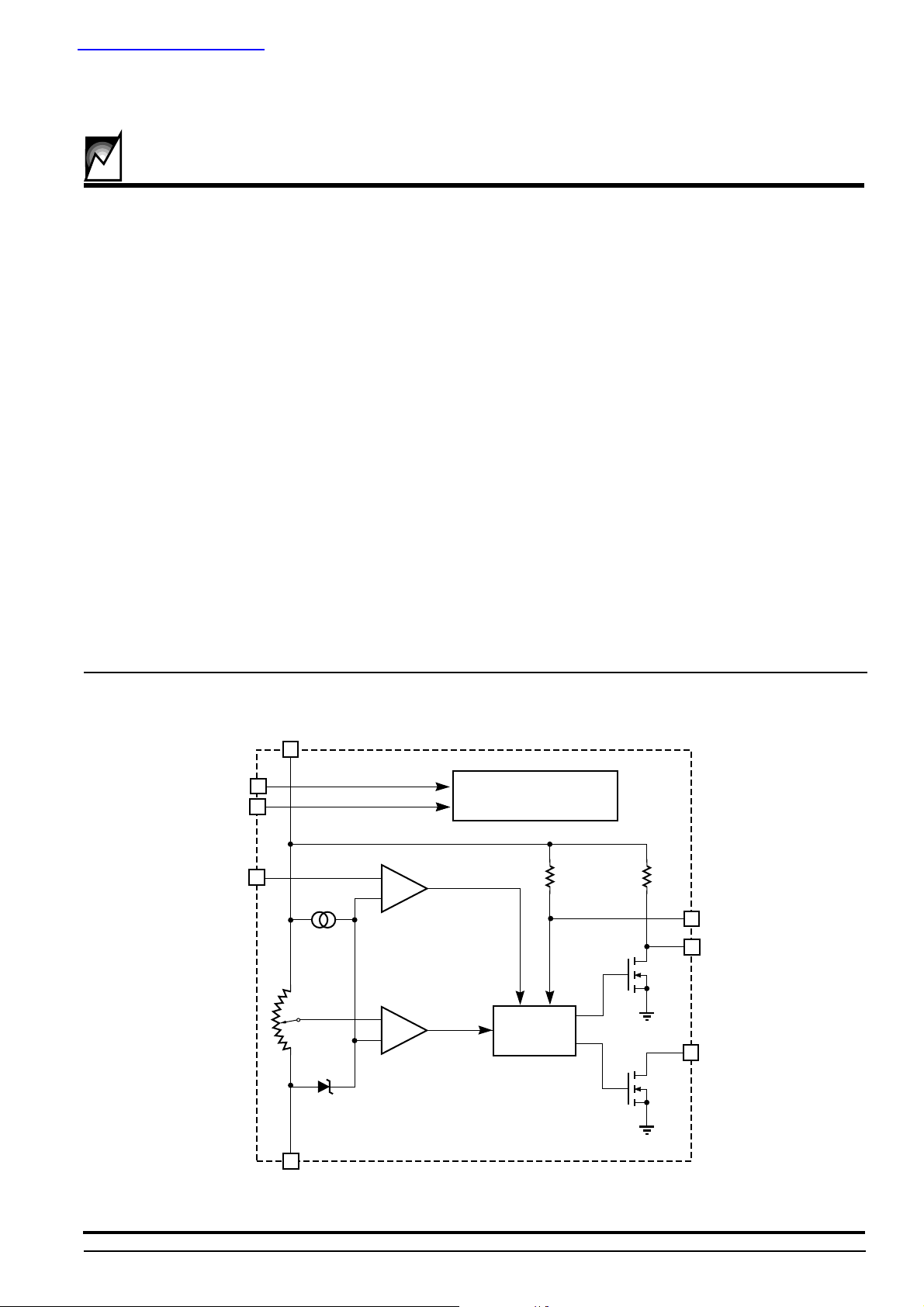
The SMS1242 microprocessor supervisory circuit reduces the complexity and number of components required
to monitor the supply voltage in +5V, +3V and +2.5V
systems. The SMS1242 will significantly improve system
reliability and accuracy when compared to implementing
the same functions with discrete components.
The SMS1242 provides reset output during power-up,
power-down, and brown-out conditions. It has a 1.25V
threshold input detector for power-fail warning, low battery
detection, or monitoring a secondary power supply. The
part also integrates a separate active low manual reset
input.
It also has 16k-bits of nonvolatile memory accessible over
an industry standard 2-wire serial interface.
FUNCTIONAL BLOCK DIAGRAM
+
–
GND
V
CC
8
4
RESET1#
2
V
TRIP
RESET
GENERATOR
7
1.25V
SCL
6
SDA
5
2038 BD 2.0
NONVOLATILE
MEMORY
ARRAY
V
SENSE
3
MR#
1
+
–
RESET2#
查询SMS1242S-F供应商
Page 2
2
SMS1242
2038 2.0 6/8/00SUMMIT MICROELECTRONICS, Inc.
ABSOLUTE MAXIMUM RATINGS*
Temperature Under Bias –55°C to 125°C
Storage Temperature –65°C to 150°C
Terminal Voltage (With Respect to Ground)–0.3V to 6V
Lead Solder Temperature (10 secs) 300°C
*COMMENT
Stresses above those listed under Absolute Maximum Ratings
may cause permanent damage to the device. These are stress
ratings only, and functional operation of the device at these or
any other conditions outside those listed in the operation sections of this specification is not implied. Exposure to any absolute maximum rating for extended periods may affect device
performance and reliability.
2038 Elect Table 2.0
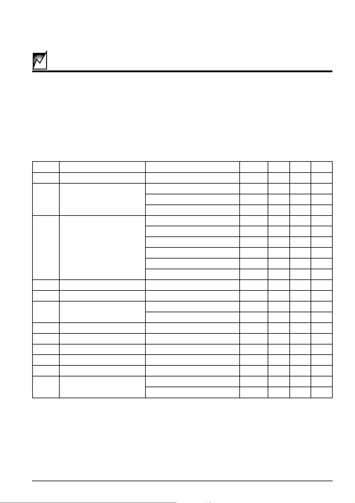
lobmySretemaraPsnoitidnoC.niM.pyT.xaMstinU
V
CC
egatlovylppusgnitarepO15.5V
I
CC
tnerrucylppuS
<V6.3V
CC
5.5<V 5205Aµ
>V6.3V
CC
5205Aµ
)ylno3421SMS(sseccayromeM3Am
V
TSR
dlohserhtteseR
AnoitpoeciveD573.4524.4574.4V
BnoitpoeciveD526.4576.4527.4V
CnoitpoeciveD524.4574.4525.4V
DnoitpoeciveD524.2054.2574.2V
EnoitpoeciveD526.2056.2576.2V
FnoitpoeciveD529.2059.2579.2V
V
TSYH
V
TSR
sisiretsyH 05Vm
t
TSR
htdiweslupteseR001051002sm
V
LO
egatlovwoltuptuo#1TESER
I
KNIS
V,Am2.1=
CC
V=
TSR
.nim3.0V
I
KNIS
V,Aµ002=
CC
V2.1=3.0V
I
RM
tnerrucpullup#RM 001Aµ
t
RM
htdiweslup#RM05sn
V
LI
dlohserhttupni#RM 6.0V
V
HI
dlohserhttupni#RM7.0 × V
CC
V
V
SNS
V
ESNES
dlohserhttupniV
CC
=V
TSR
V,.nim
ESNES
gnillaf02.152.103.1V
V
CC
egatlovwoltuptuo#2TESER
I
KNIS
V,Am2.1=
CC
V=
TSR
.nim3.0V
I
KNIS
V,Aµ002=
CC
V2.1=4.0V
Page 3
3
2038 2.0 6/8/00
SMS1242
SUMMIT MICROELECTRONICS, Inc.
PIN CONFIGURATION
PIN NAMES
2038 Pin Table 2.0
RESET1#
RESET2#
V
SENSE
GND
V
CC
MR#
SCL
SDA
1
2
3
4
8
7
6
5
8-Pin SOIC
2038 T PCon 2.0
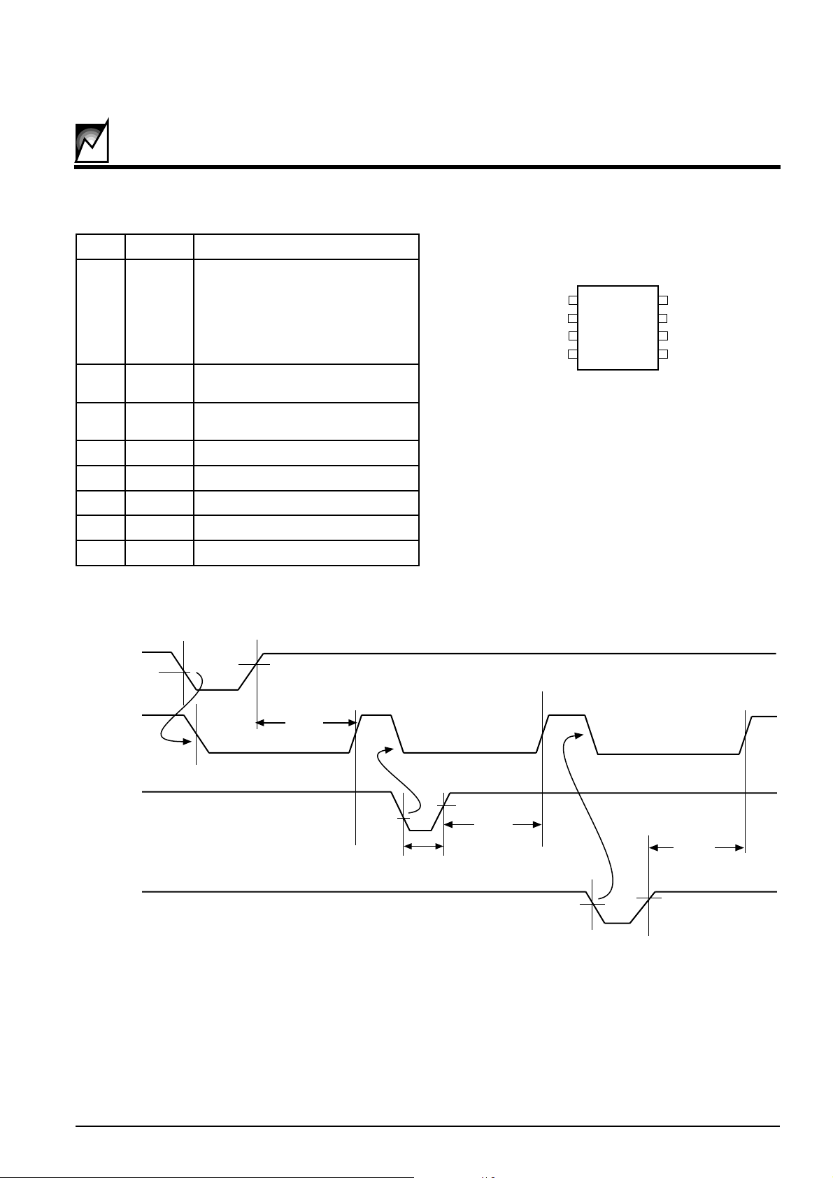
Figure 1. Reset Waveforms
niPlangiSnoitcnuF
1#1TESER
.pullupkaewhtiwtuptuowolevitcA
:ybwolnevirDV
ESNES
-hserhtwoleb
ro;dloV
CC
elihwdlohserhtwoleb
sniameR.dlohserhtwolebsi#RM
retfasm051rofwolV
ESNES
ro,V
CC
.dlohserhtevobasi,#RMdna
2#2TESER
nepotpecxe,#1teseRsaemaS
noitcennocniard
3V
ESNES
ehtroftupnirotceteddlohserhT
steseR
4DNGdnuorG
5DNG/ADSdnuorgro,O/IataD3421SMS
6DNG/LCSdnuorgro,kcolCataD3421SMS
7#RMsteseRroftupnilaunaM
8V
CC
egatlovylppuS
V
CC
RESET#
MR#
V
SENSE
V
RST
V
RST
t
RST
t
RST
t
RST
V
SNS
V
IL
V
IH
t
MR
2038 T Fig01 2.0
Page 4
4
SMS1242
2038 2.0 6/8/00SUMMIT MICROELECTRONICS, Inc.
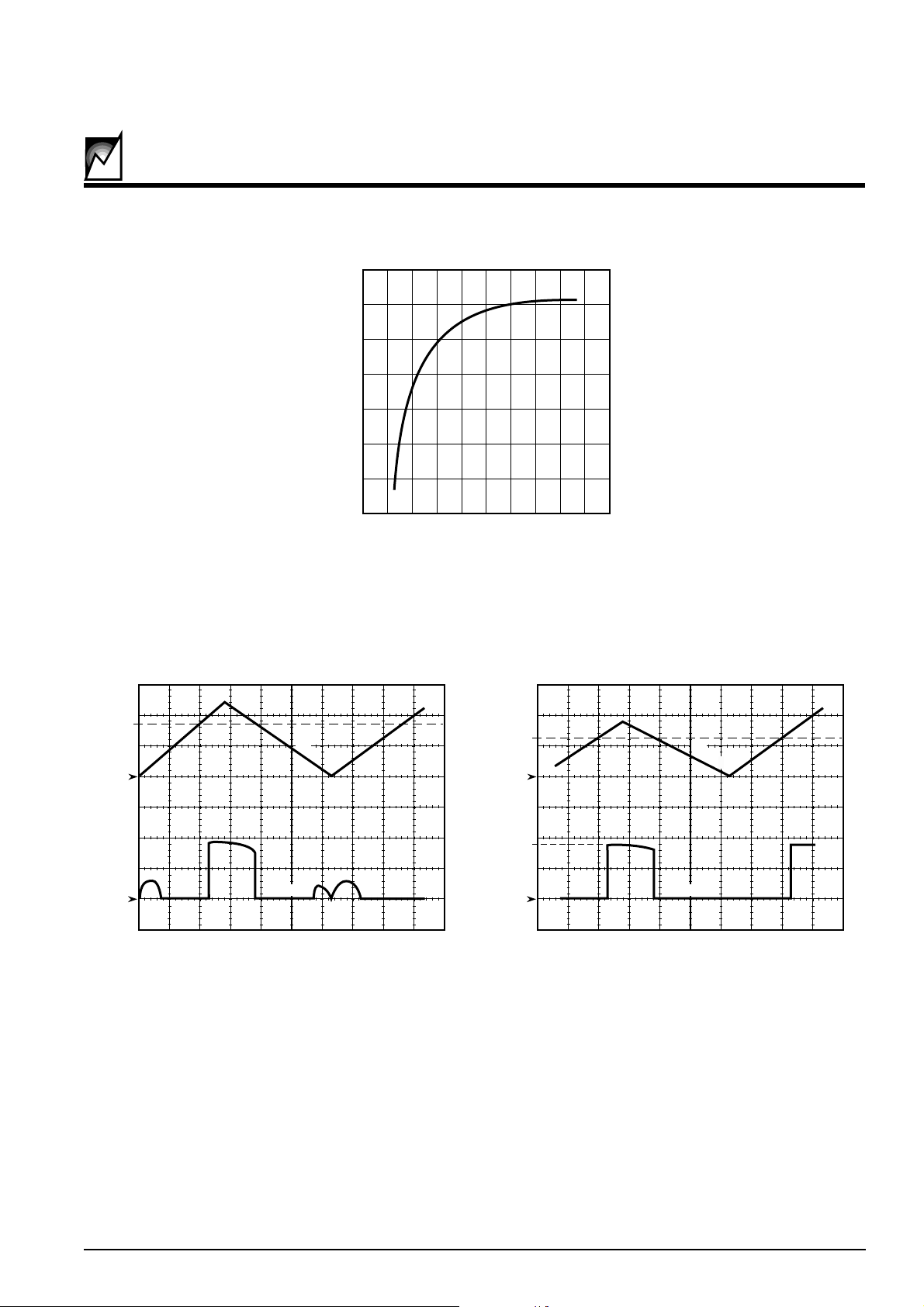
Figure 4. RESET Output vs. V
SENSE
Figure 3. RESET Output vs. Supply
Figure 2. Supply Voltage Noise Rejection, V
RST
=4.55V, TA = 25ºC
02
6
108
4
31
75
9
GLITCH AMPLITUDE (V)
PULSE WIDTH (ms)
4.5
4.4
4.3
4.2
4.1
4.0
3.9
3.8
2038 Fig02 2.0
V
RST
0V
0V
RESET#
V
CC
500ms/Div.
1.25V
0V
2V
0V
RESET#
V
SENSE
V
CC
Page 5
5
2038 2.0 6/8/00
SMS1242
SUMMIT MICROELECTRONICS, Inc.
DEVICE OPERATION
The SMS1242 provides a precision reset function for a
microcontroller or microprocessor during power-up,
power-down and brown-out conditions. The device will
monitor two independent voltage supplies and will generate a reset condition when either supply is invalid. It is
configured with two outputs, both driven by the same
conditions. They are open drain and will track each other
but the outputs are not internally tied together.
Because RESET1# and RESET2# are essentially open
drain outputs (RESET1# has a weak internal pullup,
RESET2# does not) they can be independently driven low
by external signals. This can be very useful in a dual
processor system or in a combined processor/ASIC system where, either for system operation or system test, the
processors or ASICs must be independently held in reset
without resetting the other portion of the system.
SUPPLY MONITOR
(Assume V
SENSE
> V
SNS
) During power-up the SMS1242
monitors the supply voltage. The RESET1# and RESET2# outputs are guaranteed to be driven low once V
CC
reaches 1V. As VCC rises RESET1# and RESET2#
remain asserted until VCC reaches the V
RST
threshold. As
VCC passes through V
RST
an internal timer is started to
continue driving the outputs for an additional 150ms
(nominal).
If a power-fail or brown-out condition occurs (VCC < V
RST
)
RESET1# and RESET2# will be asserted. They will
remain active so long as VCC is below V
RST
. Because the
internal timer will be continuously reset so long as VCC is
below V
RST
, a brownout condition that interrupts a previously initiated reset pulse causes an additional reset delay
from the time the VCC passes back through V
RST
.
During power down conditions, once VCC drops below
V
RST
, RESET1# and RESET2# are guaranteed to be
asserted for VCC ≥ 1V.
V
SENSE
MONITOR
(Assume VCC is >V
RST
) The SMS1242 continuously
monitors the VSENSE input. The RESET1# and RESET2# outputs will be driven low so long as V
SENSE
is <
VSNS. As V
SENSE
passes through V
SNS
an internal timer
is started to continue driving the outputs for an additional
150ms (nom.).
If a power-fail condition occurs (V
SENSE
falls below V
SNS
)
RESET1# and RESET2# will be asserted. They will remain active so long as V
SENSE
is below V
SNS
. Because
the internal timer will be continuously reset so long as
V
SENSE
is below V
SNS
, a brownout condition that interrupts a previously initiated reset pulse causes an additional reset delay from the time V
SENSE
becomes greater
than V
SNS
.
MANUAL RESET
The manual reset input allows RESET1# and RESET2# to
be activated by a pushbutton switch. The switch is
effectively debounced by the 100ms minimum t
RST
(RESET pulse width). MR# can also be driven by an external
logic input that meets the 50ns minimum pulse width
required.
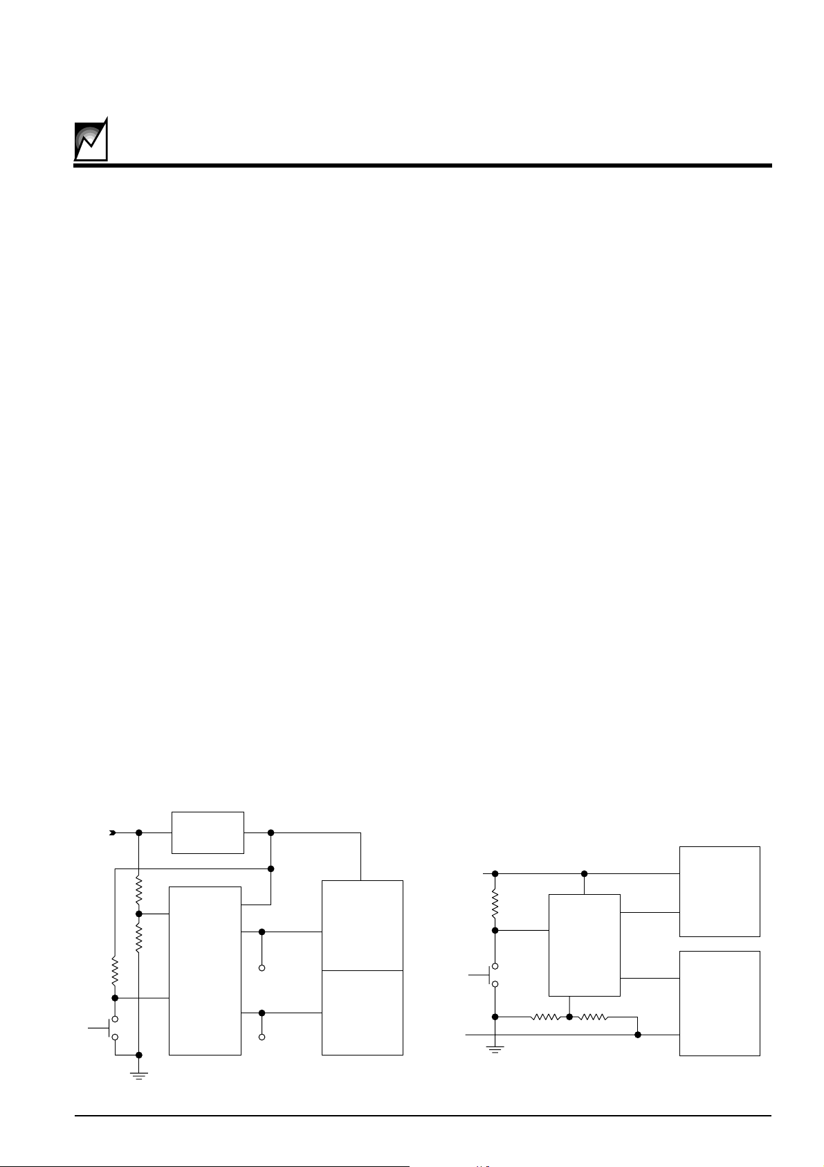
MCU #1
ASIC or MCU #2
RESET2#
RESET1#
VCC
Unregulated
+12V DC
DC to DC
Converter
3.3V Out
VSENSE
MR#
Test Point #1
Test Point #2
SMS1242
2038 ILL7.0
MCU
Low Voltage
High Speed
ASIC
RESET2#
RESET1#
VCC
3.3V
VSENSE
MR#
SMS1242
1.8V
2038 ILL8.0
Figure 5. Typical Multi-MCU Implementation
Figure 6. Typical Dual Voltage Implementation
Page 6
6
SMS1242
2038 2.0 6/8/00SUMMIT MICROELECTRONICS, Inc.
2038 Table01 2.0
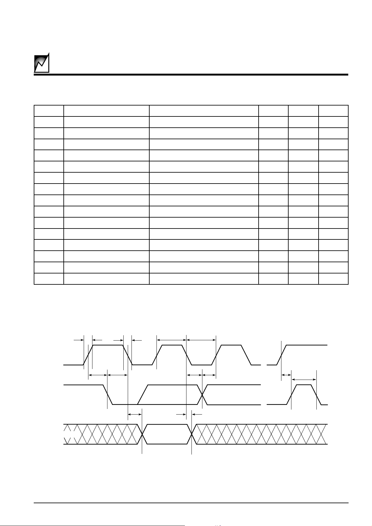
Figure 7. Memory Timing
lobmySretemaraPsnoitidnoC.niM.xaMstinU
f
LCS
ycneuqerfkcolcLCS 0001zHk
t
WOL
doirepwolkcolC 7.4sµ
t
HGIH
doirephgihkcolC 0.4sµ
t
FUB
emiteerfsuBnoissimsnartwenerofeB7.4sµ
t
ATS:US
emitputesnoitidnoctratS 7.4sµ
t
ATS:DH
emitdlohnoitidnoctratS 0.4sµ
t
OTS:US
emitputesnoitidnocpotS 7.4sµ
t
AA
tuptuodilavotegdekcolC)nelcyc(ADSdilavotwolLCS3.05.3sµ
t
HD
emitdlohtuOataDegnahcADSot)1+nelcyc(wolLCS3.0sµ
t
R
emitesirADSdnaLCS 0001sn
t
F
emitllafADSdnaLCS 003sn
t
TAD:US
emitputesnIataD 052sn
t
TAD:DH
emitdlohnIataD 0sn
ITADSdnaLCSretlifesioNnoiserppusesioN001sn
t
RW
emitelcycetirW 5sm
t
F
t
R
t
LOW
t
HIGH
t
HD:SDA
t
SU:SDA
t
BUF
t
DH
t
HD:DAT
t
SU:DAT
t
SU:STO
SCL
SDA In
SDA Out
t
AA
2038 Fig07 2.0
Page 7
7
2038 2.0 6/8/00
SMS1242
SUMMIT MICROELECTRONICS, Inc.
MEMORY OPERATION
The SMS1242 memory is configured as a 2k × 8 array.
Data is read and written via an industry standard two-wire
interface. The bus was designed for two-way, two-line
serial communication between different integrated circuits. The two lines are a serial data line (SDA) and a serial
clock line (SCL). The SDA line must be connected to a
positive supply by a pull-up resistor located somewhere on
the bus
Input Data Protocol
The protocol defines any device that sends data onto the
bus as a “transmitter” and any device that receives data as
a “receiver.” The device controlling data transmission is
called the “master” and the controlled device is called the
“slave.” In all cases the SMS1242 will be a “slave” device
since it never initiates a data transfer.
One data bit is transferred during each clock pulse. The
data on the SDA line must remain stable during clock high
time, because changes on the data line while SCL is high
will be interpreted as start or stop condition.
START and STOP Conditions
When both the data and clock lines are high the bus is said
to be not busy. A high-to-low transition on the data line
while the clock is high is defined as the “START” condition.
A low-to-high transition on the data line while the clock is
high is defined as the “STOP” condition.
Acknowledge (ACK)
Acknowledge is a software convention used to indicate
successful data transfers. The transmitting device, either
the master or the slave, will release the bus after transmitting eight bits. During the ninth clock cycle the receiver will
pull the SDA line low to ACKnowledge that it received the
eight bits of data.
The SMS1242 will respond with an ACKnowledge after
recognition of a START condition and its slave address
byte. If both the device and a write operation are selected,
the SMS1242 will respond with an ACKnowledge after the
receipt of each subsequent 8-bit word. In the READ mode
the SMS1242 transmits eight bits of data, then releases
the SDA line, and monitors the line for an ACKnowledge
signal. If an ACKnowledge is detected and no STOP
condition is generated by the master, the SMS1242 will
continue to transmit data. If an ACKnowledge is not
detected the SMS1242 will terminate further data transmissions and await a STOP condition before returning to
the standby power mode.
Device Addressing
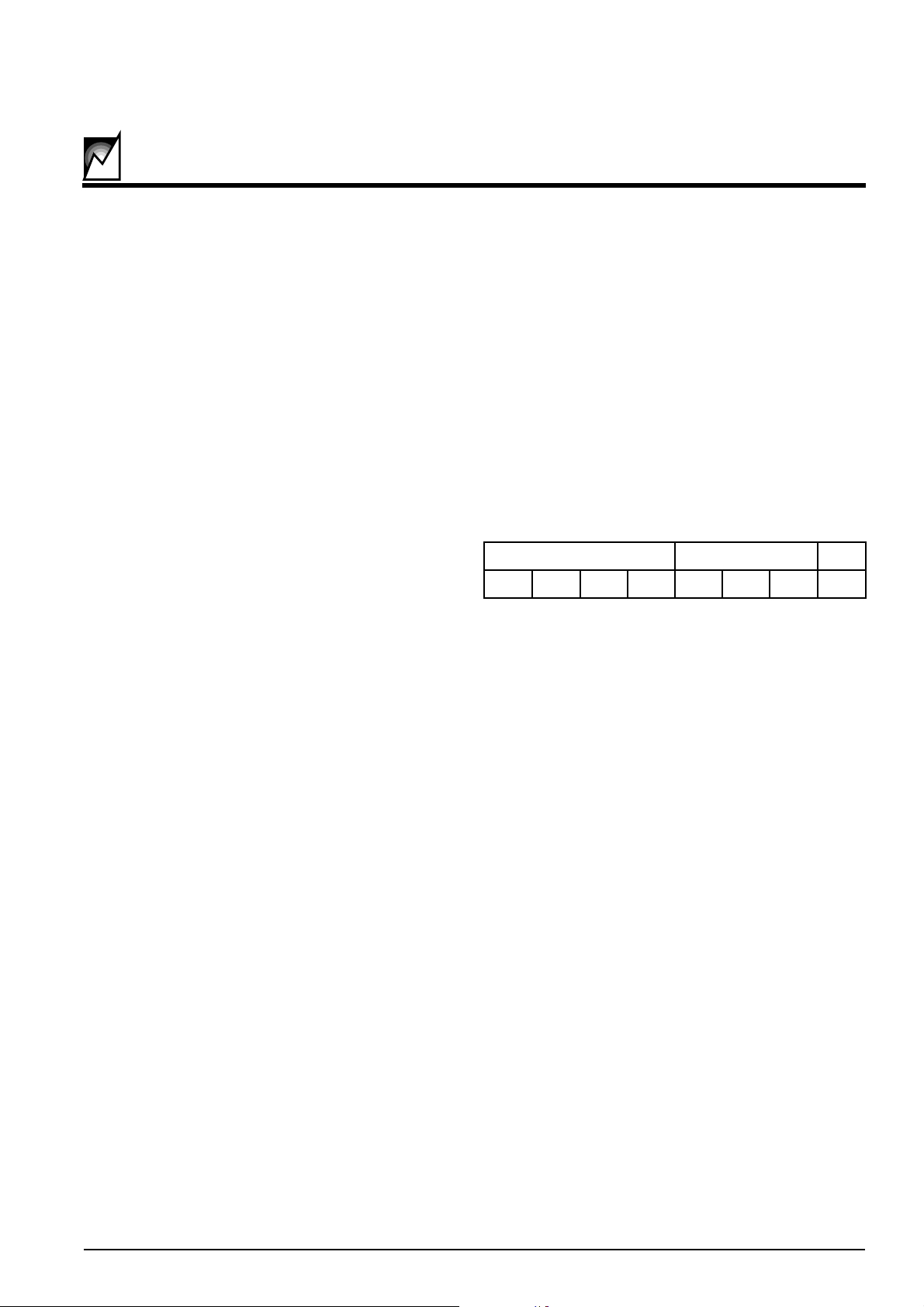
Following a start condition the master must output the
address of the slave it is accessing. The most significant
four bits of the slave address are the device type identifier.
For the SMS1242 this is fixed as 1010
BIN
. The next three
bits are the Most Significant Bits of the data address. They
are supplied for write operations, and are "don't care" for
read operations.
Read/Write Bit
The last bit of the data stream defines the operation to be
performed. A “1” indicates a read operation; and a “0,” a
write operation.
2038 Table02 2.0
reifitnedIeciveDstiBsserddASMW/R
10 10 01A9A8A0/1
WRITE OPERATIONS
The SMS1242 allows two types of write operations: byte
write and page write. A byte write operation writes a single
byte during the nonvolatile write period (tWR). The page
write operation allows up to 16 bytes in the same page to
be written during tWR.
Byte Write
Upon receipt of the word address the SMS1242 responds
with an ACKnowledge. After receiving the next byte of
data it responds with another ACKnowledge. The master
then terminates the transfer by generating a STOP condition, at which time the SMS1242 begins the internal write
cycle. While the internal write cycle is in progress the
SMS1242 inputs are disabled and the device will not
respond to any requests from the master.
Page Write
The SMS1242 is capable of a 16-byte page write operation. It is initiated in the same manner as the byte-write
operation, but instead of terminating the write cycle after
the first data word the master can transmit up to 15 more
bytes of data. After the receipt of each byte the SMS1242
will respond with an ACKnowledge.
The SMS1242 automatically increments the address for
subsequent data words. After the receipt of each word, the
low order address bits are internally incremented by one.
The high order bits of the address byte remain constant.
Page 8
8
SMS1242
2038 2.0 6/8/00SUMMIT MICROELECTRONICS, Inc.
Next
Operation
a Write?
ACK
Returned
Issue
Address
Proceed
With
Write
Await
Next
Command
Issue Stop
Issue Slave
Address and
R/W = 0
Issue Stop
Write Cycle
In Progress
Yes
No
Issue Start
2038 Flow01 2.0
Yes
No
Should the master transmit more than 16 bytes, prior to
generating the STOP condition, the address counter will
“roll over” and the previously written data will be overwritten. As with the byte-write operation, all inputs are
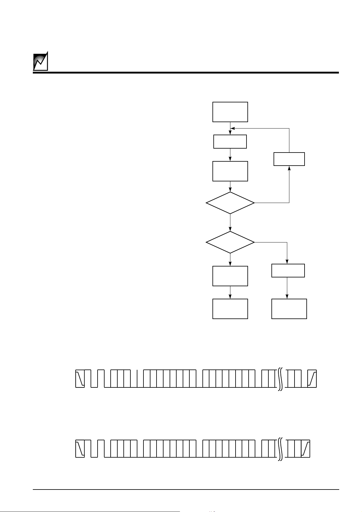
disabled during the internal write cycle. Refer to Figure 8
for the address, ACKnowledge and data transfer sequence.
Acknowledge Polling
When the SMS1242 is performing an internal WRITE
operation it will ignore any new START conditions. Since
the device will only return an acknowledge after it accepts
the START, the part can be continuously queried until an
acknowledge is issued, indicating that the internal WRITE
cycle is complete. See the flow diagram for the proper
sequence of operations for polling.
READ OPERATIONS
Read operations are initiated with the R/W bit of the
identification field set to “1.” There are two different read
options:
1. Current Address Byte Read
2. Random Address Byte Read
Current Address Read
The SMS1242 contains an internal address counter which
maintains the address of the last word accessed, incremented by one. If the last address accessed (either a read
Figure 8. Memory Operation
A
C
K
X X
X
R
/
W
A
C
K
D7D6D5D4D3D2D1D
0
A
C
K
D7D
6
D1D
0
S
T
O
P
S
T
A
R
T
D7D6D5D4D3D2D1D
0
S
T
A
R
T
A
C
K
R
/
W
A7A6A5A4A3A2A1A
0
A
C
K
D7D6D5D4D3D2D1D
0
A
C
K
D7D
6
D1D
0
A
C
K
S
T
O
P
Typical Write Operation
Typical Read Operation
Master
SDA
Slave
Master
SDA
Slave
2038 T Fig08 2.0
A
1
0
A
9
A
8
MEMORY OPERATION (Continued)
Page 9

9
2038 2.0 6/8/00
SMS1242
SUMMIT MICROELECTRONICS, Inc.
or write) was to address location n, the next read operation
would access data from address location n+1 and increment the current address pointer. When the SMS1242
receives the slave address field with the R/W bit set to “1”
it issues an acknowledge and transmits the 8-bit word
stored at address location n+1. The current address byte
read operation only accesses a single byte of data. The
master does not acknowledge the transfer, but does
generate a stop condition. At this point, the SMS1242
discontinues data transmission.
Random Address Read
Random address read operations allow the master to
access any memory location in a random fashion. This
operation involves a two-step process. First, the master
issues a write command which includes the start condition
and the slave address field (with the R/W bit set to WRITE),
followed by the address of the word it is to read. This
procedure sets the internal address counter of the
SMS1242 to the desired address. After the word address
acknowledge is received by the master it immediately
reissues a start condition followed by another slave address field with the R/W bit set to READ. The SMS1242
will respond with an acknowledge and then transmit the 8data bits stored at the addressed location. At this point, the
master does not acknowledge the transmission but does
generate the stop condition. The SMS1242 discontinues
data transmission and reverts to its standby power mode.
Sequential READ
Sequential reads can be initiated as either a current
address READ or a random access READ. The first word
is transmitted as with the other byte read modes (current
address byte READ or random address byte READ);
however, the master now responds with an ACKnowledge, indicating that it requires additional data from the
SMS1242. The SMS1242 continues to output data for
each ACKnowledge received. The master terminates the
sequential READ operation by not responding with an
ACKnowledge, and issues a STOP condition. During a
sequential read operation, the internal address counter is
automatically incremented with each ACKnowledge signal. For read operations, all address bits are incremented,
allowing the entire array to be read using a single read
command. After a count of the last memory address, the
address counter will roll-over, and the memory will continue to output data.
Page 10
10
SMS1242
2038 2.0 6/8/00SUMMIT MICROELECTRONICS, Inc.
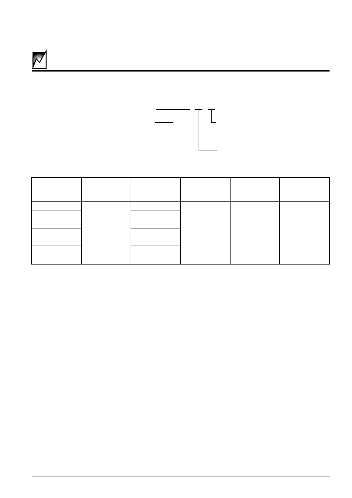
ORDERING INFORMATION
SMS1242
S
A
Base Part Number
Option
See Option Table
Package
S = SOIC
2038 Option Table 2.0
Table 3. Order Options
rebmuNtraP
gnitarepO
egatloV
V
TSR
V
SNS
gnitarepO
erutarepmeT
egnaR
&tnuoCdaeL
elytSegakcaP
A-S2421SMS
V5.5otV1
524.4
V52.1Cº58otCº04– CIOSniP8
B-S2421SMS574.4
C-S2421SMS676.4
D-S2421SMS054.4
E-S2421SMS056.2
F-S2421SMS059.2
*-S2421SMS*GORP
Page 11
11
2038 2.0 6/8/00
SMS1242
SUMMIT MICROELECTRONICS, Inc.
NOTICE
SUMMIT Microelectronics, Inc. reserves the right to make changes to the products contained in this publication in order to improve
design, performance or reliability. SUMMIT Microelectronics, Inc. assumes no responsibility for the use of any circuits described
herein, conveys no license under any patent or other right, and makes no representation that the circuits are free of patent
infringement. Charts and schedules contained herein reflect representative operating parameters, and may vary depending upon
a user’s specific application. While the information in this publication has been carefully checked, SUMMIT Microelectronics, Inc.
shall not be liable for any damages arising as a result of any error or omission.
SUMMIT Microelectronics, Inc. does not recommend the use of any of its products in life support applications where the failure or
malfunction of the product can reasonably be expected to cause failure of the life support system or to significantly affect its safety
or effectiveness. Products are not authorized for use in such applications unless SUMMIT Microelectronics, Inc. receives written
assurances, to its satisfaction, that: (a) the risk of injury or damage has been minimized; (b) the user assumes all such risks; and
(c) potential liability of SUMMIT Microelectronics, Inc. is adequately protected under the circumstances.
© Copyright 2000 SUMMIT Microelectronics, Inc.
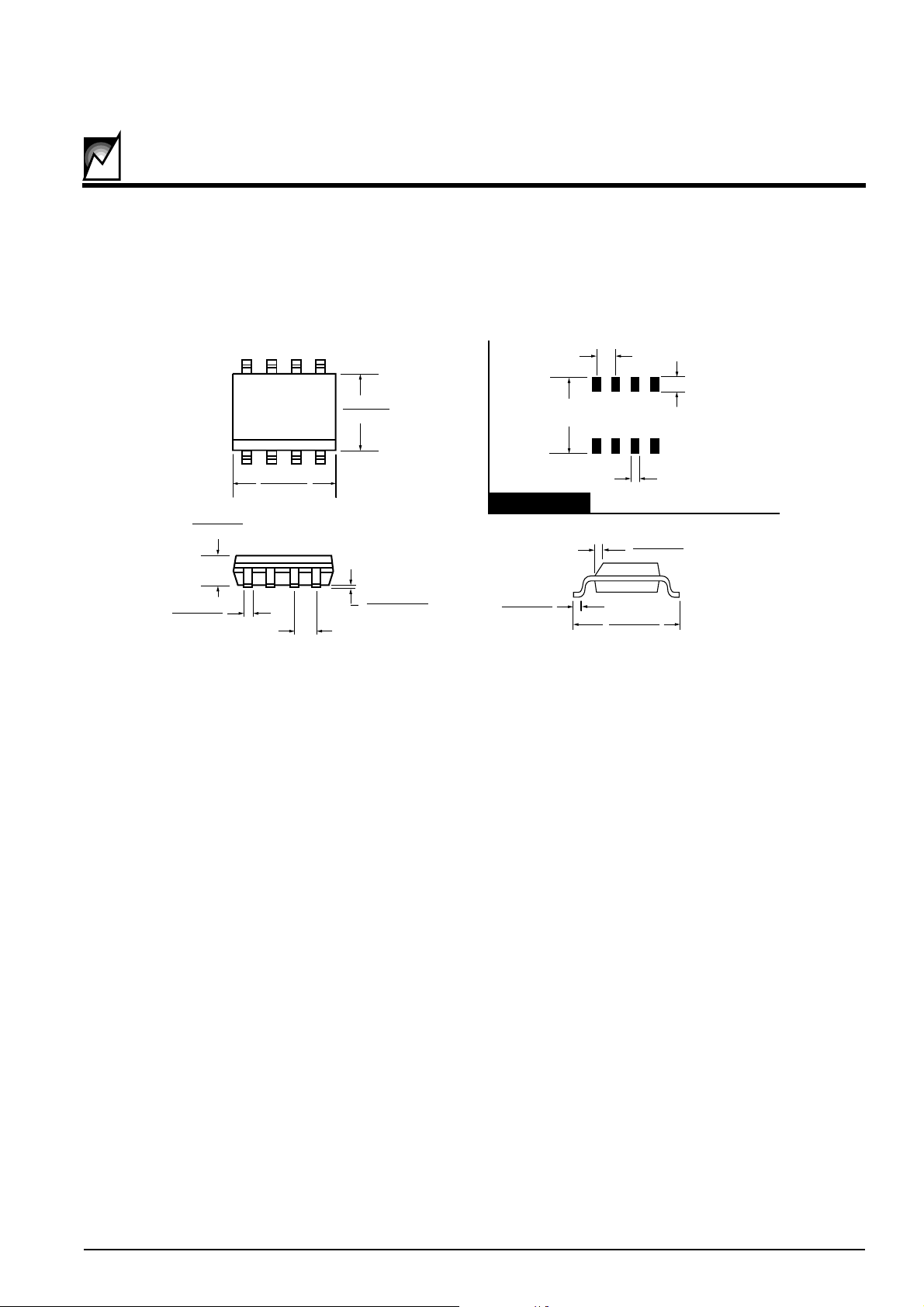
.228 (5.80)
.244 (6.20)
.016 (.40)
.035 (.90)
.020 (.50)
.010 (.25)
x45°
.0192 (.49)
.0138 (.35)
.061 (1.75)
.053 (1.35)
.0098 (.25)
.004 (.127)
.05 (1.27) TYP.
.275 (6.99) TYP.
.030 (.762) TYP.
8 Places
.050 (1.27) TYP.
.050 (1.270) TYP.
8 Places
.157 (4.00)
.150 (3.80)
.196 (5.00)
1
.189 (4.80)
FOOTPRINT
8pn JEDEC SOIC ILL.2
8 Pin SOIC (Type S) Package JEDEC (150 mil body width)
PACKAGE
 Loading...