

Page 1
查询SMP100LC供应商
®
TRISIL™ FOR TELECOM EQUIPMENT PROTECTION
FEATURES
■ Bidirectional crowbar protection
■ Voltage range from 8V to 400V
■ Low capacitance from 20pF to 45pF @ 50V
■ Low leakage current : I
■ Holding current: I
■ Repetitive peak pulse current:
I
= 100 A (10/1000µs)
PP
MAIN APPLICATIONS
Any sensitive equipment requiring protection
against lightning strikes and power crossing.
These devices are dedicated to central office protection as they comply with the most stressfull
standards.
Their Low Capacitances make them suitable for
ADSL.
DESCRIPTION
The SMP100LC is a series of low capacitance
transient surge arrestors designed for the protection of high debit rate communication equipment.
Its low capacitance avoids any distortion of the signal and is compatible with digital transmission line
cards (xDSL, ISDN...).
SMP100LC series tested and confirmed compatible with Cooper Bussmann Telecom Circuit Protector TCP 1.25A.
BENEFITS
Trisils are not subject to ageing and provide a fail
safe mode in short circuit for a better protection.
They are used to help equipment to meet main
standards such as UL60950, IEC950 / CSA C22.2
and UL1459. They have UL94 V0 approved resin.
SMB package is JEDEC registered (DO-214AA).
Trisils comply with the following standards GR1089 Core, ITU-T-K20/K21, VDE0433, VDE0878,
IEC61000-4-5 and FCC part 68.
= 2µA max
R
= 150 mA min
H
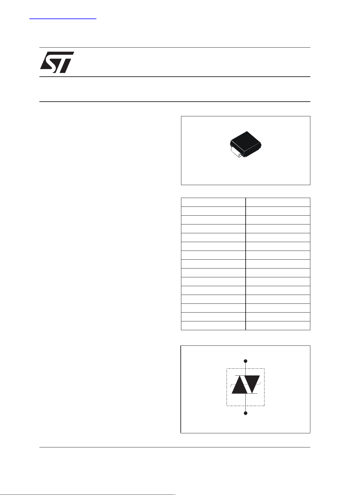
SMP100LC
SMB
(JEDEC DO-214AA)
Table 1: Order Codes
Part Number Marking
SMP100LC-8 PL8
SMP100LC-25 L25
SMP100LC-35 L35
SMP100LC-65 L06
SMP100LC-90 L09
SMP100LC-120 L12
SMP100LC-140 L14
SMP100LC-160 L16
SMP100LC-200 L20
SMP100LC-230 L23
SMP100LC-270 L27
SMP100LC-320 L32
SMP100LC-360 L36
SMP100LC-400 L40
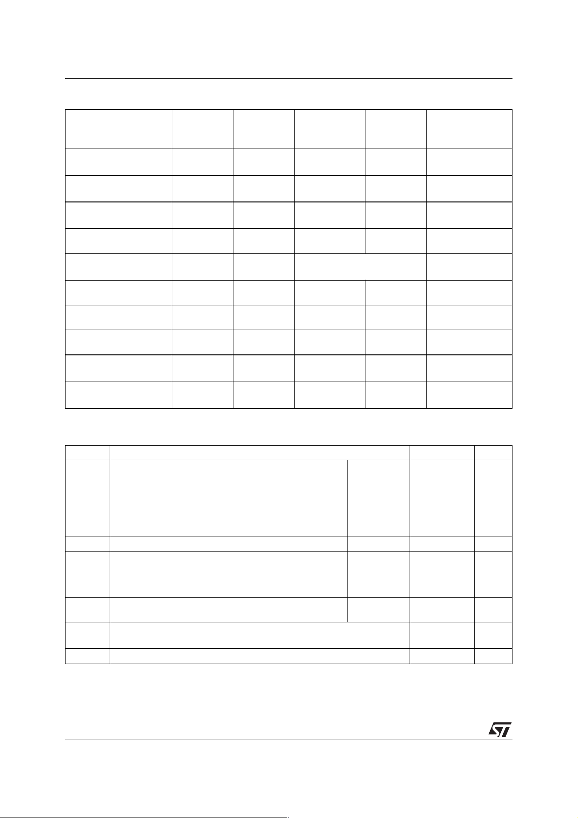
Figure 1: Schematic Diagram
June 2005
REV. 11
1/10
Page 2
SMP100LC
Table 2: In compliance with the following standards
STANDARD
GR-1089 Core
First level
GR-1089 Core
Second level
GR-1089 Core
Intra-building
ITU-T-K20/K21
ITU-T-K20
(IEC61000-4-2)
VDE0433
VDE0878
IEC61000-4-5
FCC Part 68, lightning
surge type A
FCC Part 68, lightning
surge type B
Peak Surge
Voltag e
(V)
2500
1000
5000 2/10 µs 500 2/10 µs 0
1500 2/10 µs 100 2/10 µs 0
6000
1500
8000
15000
4000
2000
4000
2000
4000
4000
1500
800
1000 9/720 µs 25 5/320 µs 0
Waveform
Voltag e
2/10 µs
10/1000 µs
10/700 µs
1/60 ns
10/700 µs
1.2/50 µs
10/700 µs
1.2/50 µs
10/160 µs
10/560 µs
Required
peak current
(A)
500
100
150
37.5
Current
waveform
2/10 µs
10/1000 µs
5/310 µs
ESD contact discharge
ESD air discharge
100
50
100
50
100
100
200
100
5/310 µs
1/20 µs
5/310 µs
8/20 µs
10/160 µs
10/560 µs
Minimum serial
resistor to meet
standard (Ω)
0
0
0
0
0
0
0
0
0
0
0
0
0
0
Table 3: Absolute Ratings (T
amb
= 25°C)
Symbol Parameter Value Unit
I
PP
I
FS
I
TSM
I
T
T
T
Note 1: in fail safe mode, the device acts as a short circuit
Repetitive peak pulse current (see figure 2) 10/1000 µs
Fail-safe mode : maximum current (note 1)
Non repetitive surge peak on-state current (sinusoidal) t = 0.2 s
2
tI2t value for fusing
Storage temperature range
stg
Maximum junction temperature
j
Maximum lead temperature for soldering during 10 s.
L
8/20 µs
10/560 µs
5/310 µs
10/160 µs
1/20 µs
2/10 µs
8/20 µs 5
t = 1 s
t = 2 s
t = 15 mn
t = 16.6 ms
t = 20 ms
100
400
140
150
200
400
500
24
15
12
4
20
21
-55 to 150
150
260
A
A
kA
A
°C
°C
2
s
2/10
Page 3
SMP100LC
Table 4: Thermal Resistances
Symbol Parameter Value Unit
R
R
th(j-a)
th(j-l)
Junction to ambient (with recommended footprint) 100 °C/W
Junction to leads 20 °C/W
Table 5: Electrical Characteristics (T
amb
= 25°C)
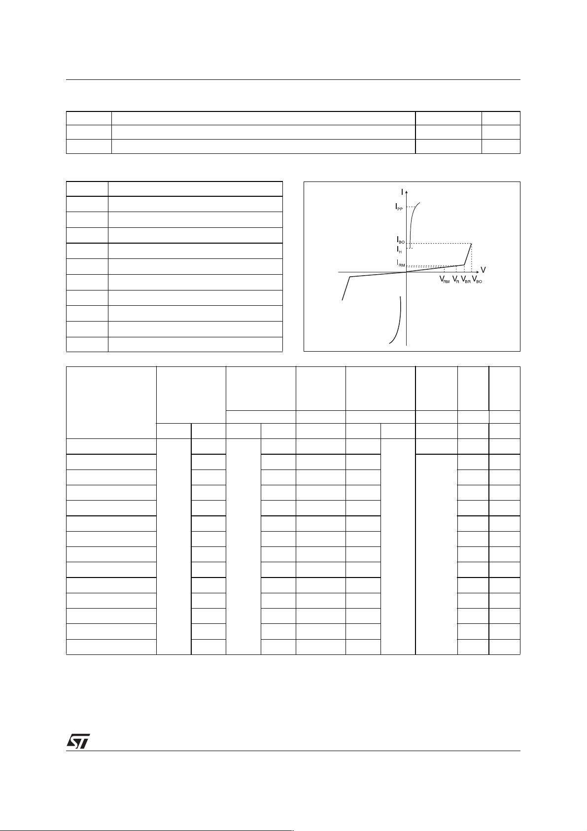
Symbol Parameter
V
V
V
I
I
I
Stand-off voltage
RM
Breakdown voltage
BR
Breakover voltage
BO
Leakage current
RM
Peak pulse current
PP
Breakover current
BO
I
Holding current
H
V
Continuous reverse voltage
R
Leakage current at V
I
R
R
C Capacitance
Types
I
RM
@ V
RM
IR @ V
R
Dynamic
V
BO
max. max. max. max. max. min. typ. typ.
note1 note 2 note 3 note 4 note 5 note 6
V
BO
Static
@ I
BO
I
H
CC
µAVµAV V VmAmApFpF
SMP100LC-8
SMP100LC-25 22 25 40 35
6
82515
50 (typ.) NA 75
NA 65
SMP100LC-35 32 35 55 55 NA 55
SMP100LC-65 55 65 85 85 45 90
SMP100LC-90 81 90 120 125 40 80
SMP100LC-120 108 120 155 160 35 75
SMP100LC-140 120 140 185 190 30 65
SMP100LC-160 144 160 205 200 30 65
2
5
800
150
SMP100LC-200 180 200 255 250 30 60
SMP100LC-230 207 230 295 285 30 60
SMP100LC-270 243 270 345 335 30 60
SMP100LC-320 290 320 400 390 25 50
SMP100LC-360 325 360 460 450 25 50
SMP100LC-400 360 400 540 530 20 45
Note 1: IR measured at VR guarantee VBR min ≥ VR
Note 2: see functional test circuit 1
Note 3: see test circuit 2
Note 4: see functional holding current test circuit 3
Note 5: V
Note 6: V
= 50V bias, V
R
= 2V bias, V
R
RMS
=1V, F=1MHz
RMS
=1V, F=1MHz
3/10
Page 4

SMP100LC
Figure 2: Pulse waveform Figure 3: Non repetitive surge peak on-state
current versus overload duration
I (A)
TSM
70
60
50
40
30
20
10
0
1E-2 1E-1 1E+0 1E+1 1E+2 1E+3
t(s)
F=50Hz
T initial = 25°C
j
100
50
0
%I
PP
Repetitive peak pulse current
tr = rise time (µs)
tp = pulse duration time (µs)
t
r
t
p
t
Figure 4: On-state voltage versus on-state
current (typical values)
I (A)
T
100
V (V)
10
012345678
T
T initial = 25°C
j
Figure 6: Relative variation of breakover
voltage versus junction temperature
V [ ] / V [ =25°C]
TT
BO BO
1.08
1.06
1.04
1.02
jj
Figure 5: Relative variation of holding current
versus junction temperature
I [T ] / I [T =25°C]
HH
jj
2.0
1.8
1.6
1.4
1.2
1.0
0.8
0.6
0.4
0.2
0.0
-25 0 25 50 75 100 125
T (°C)
j
Figure 7: Relative variation of leakage current
versus junction temperature (typical values)
I [ ] / I [ =25°C]
TT
RR
2000
1000
jj
100
1.00
0.98
0.96
4/10
T (°C)
j
-25 0 25 50 75 100 125
10
T (°C)
1
25 50 75 100 125
j
Page 5

SMP100LC
Figure 8: Variation of thermal impedance
junction to ambient versus pulse duration
(Printed circuit board FR4, SCu=35µm,
Figure 9: Relative variation of junction
capacitance versus reverse voltage applied
(typical values)
recommended pad layout)
C [V ] / C [V =2V]
Z/R
th(j-a) th(j-a)
100
10
t (s)
1
1E-3 1E-2 1E-1 1E+0 1E+1 1E+2 5E+2
p
RR
1.4
1.2
1.0
0.8
0.6
0.4
0.2
0.0
12
F =1MHz
V= 1V
RMS
T = 25°C
j
V (V)
R
5 10 20 50 100 300
APPLICATION NOTE
In wireline applications, analog or digital, both central office and subscriber sides have to be protected.
This function is assumed by a combined series / parallel protection stage.
Ring
relay
Line
Protection stage
Ex. Analog line card Ex. ADSL line card or terminal
Line
Protection stage
In such a stage, parallel function is assumed by one or several Trisil, and is used to protect against short
duration surge (lightning). During this kind of surges the Trisil limits the voltage across the device to be
protected at its break over value and then fires. The fuse assumes the series function, and is used to protect the module against long duration or very high current mains disturbances (50/60Hz). It acts by safe
circuits opening. Lightning surge and mains disturbance surges are defined by standards like GR1089,
FCC part 68, ITU-T K20.
Fuse TCP 1.25A
Tip S
SMP100LC-xxx
Gnd
SMP100LC-xxx
Ring S
Fuse TCP 1.25A
Typical circuit for subscriber side
T1
SMP100LC-xxx
T2
Tip L
Gnd
Fuse TCP 1.25A
Ring L
Typical circuit for central office side
5/10
Page 6

SMP100LC
Following figure shows the test method of the
board having Fuse and Trisil.
Surge
Generator
Current probe
I surge
Line side
Test board
Oscilloscope
Device to be protected
V
Voltage probe
These topologies, using SMP100LC from ST and
TCP1.25A from Cooper Bussmann, have been
functionally validated with a Trisil glued on the
PCB. Following example was performed with
SMP100LC-270 Trisil. For more information, see
Application Note AN2064.
Following curve shows the turn on of the Trisil during
lightning surge.
I surge (100A/div)
V (50V/div)
Test conditions:
2/10µs + and -2.5 and 5kV 500A (10 pulses of each
polarity), T
amb
= 25°C
Test result:
Fuse and Trisil OK after test in accordance with
GR1089 requirements
Following curve shows Trisil action while the fuse
remains operational.
I surge (2A/div)
V (100V/div)
Test conditions:
600V 3A 1.1s (first level), T
amb
= 25°C
Test result:
Fuse and Trisil OK after test in accordance with
GR1089 requirements
In case of high current power cross test, the fuse acts
like a switch by opening the circuit.
I surge (10A/div)
V (100V/div)
Test conditions:
277V 25A (second level), T
amb
= 25°C
Test result:
Fuse safety opened and Trisil OK after test in
accordance with GR1089 requirements
6/10
Page 7

Figure 10: Test circuit 1 for Dynamic IBO and VBO parameters
100 V / µs, di /dt < 10 A / µs, Ipp = 100 A
SMP100LC
U
KeyTek 'System 2' generator with PN246I module
10 µF
1 kV / µs, di/dt < 10 A / µs, Ipp = 10 A
26 µH
U
KeyTek 'System 2' generator with PN246I module
60 µF
Figure 11: Test circuit 2 for I
2 Ω
12 Ω
and VBO parameters
BO
45 Ω
250 Ω
83 Ω
66 Ω
470 Ω
47 Ω
K
46 µH
0.36 nF
46 µH
ton = 20ms
220V 50Hz
Vout
1/4
TEST PROCEDURE
Pulse test duration (tp = 20ms):
●
for Bidirectional devices = Switch K is closed
●
for Unidirectional devices = Switch K is open
V selection:
OUT
●
Device with V < 200V V = 250 V , R1 = 140
●
Device with V 200V V = 480 V , R2 = 240
➔ Ω
BO OUT RMS
➔ Ω≥
BO OUT RMS
R1 = 140Ω
R2 = 240Ω
IBO
measurement
DUT
VBO
measurement
7/10
Page 8

SMP100LC
Figure 12: Test circuit 3 for dynamic I
V
=-48V
BAT
This is a GO-NOGO test which allows to confirm the holding current (I ) level in a
functional test circuit.
TEST PROCEDURE
1/ Adjust the current level at the I value by short circuiting the AK of the D.U.T.
2/ Fire the D.U.T. with a surge current
3/ The D.U.T. will come back off-state within 50ms maximum.
R
H
parameter
H
➔
Figure 13: Ordering Information Scheme
I=
PP
10A, 10/1000µs.
Surge generator
D.U.T
H
Trisil Surface Mount
Repetitive Peak Pulse Current
100 = 100A
Capacitance
LC = Low Capacitance
Voltage
65 = 65V
SMP 100 LC - xxx
8/10
Page 9

Figure 14: SMB Package Mechanical data
E1
D
E
A1
C
L
A2
b
Figure 15: Foot Print Dimensions (in millimeters)
2.3
SMP100LC
DIMENSIONS
REF.
A1 1.90 2.45 0.075 0.096
A2 0.05 0.20 0.002 0.008
b 1.95 2.20 0.077 0.087
c 0.15 0.41 0.006 0.016
E 5.10 5.60 0.201 0.220
E1 4.05 4.60 0.159 0.181
D 3.30 3.95 0.130 0.156
L 0.75 1.60 0.030 0.063
Millimeters Inches
Min. Max. Min. Max.
1.52 2.75
1.52
Table 6: Ordering Information
Part Number Marking Package Weight Base qty Delivery mode
SMP100LC-8 PL8
SMP100LC-25 L25
SMP100LC-35 L35
SMP100LC-65 L06
SMP100LC-90 L09
SMP100LC-120 L12
SMP100LC-140 L14
SMP100LC-160 L16
SMB 0.11 g 2500 Tape & reel
SMP100LC-200 L20
SMP100LC-230 L23
SMP100LC-270 L27
SMP100LC-320 L32
SMP100LC-360 L36
SMP100LC-400 L40
Table 7: Revision History
Date Revision Description of Changes
09-Nov-2004 9 Absolute ratings values, table 3 on page 2, updated.
07-Dec-2004 10
SMP100LC-320, SMP100LC-360 and SMP100LC-400
addition.
20-Jun-2005 11 Telecom Circuit Protector added
9/10
Page 10

SMP100LC
Information furnished is believed to be accurate and reliable. However, STMicroelectronics assumes no responsibility for the consequences
of use of such information nor for any infringement of patents or other rights of third parties which may result from its use. No license is granted
by implication or otherwise under any patent or patent rights of STMicroelectronics. Specifications mentioned in this publication are subject
to change without notice. This publication supersedes and replaces all information previously supplied. STMicroelectronics products are not
authorized for use as critical components in life support devices or systems without express written approval of STMicroelectronics.
The ST logo is a registered trademark of STMicroelectronics.
All other names are the property of their respective owners
© 2004 STMicroelectronics - All rights reserved
Australia - Belgium - Brazil - Canada - China - Czech Republic - Finland - France - Germany - Hong Kong - India - Israel - Italy - Japan -
Malaysia - Malta - Morocco - Singapore - Spain - Sweden - Switzerland - United Kingdom - United States of America
STMicroelectronics group of compagnies
www.st.com
10/10
 Loading...