

Page 1
SUMMIT
MICROELECTRONICS, Inc.
SML2108
Dual Loop Laser Diode Adaptive Power Controller
with Look Up Table
FEATURES
!!
! Dual Closed-loop Control of Laser Diode Mean
!!
Power and Extinction Ratio
!!
! Automatic Power Control (APC) with Integrated
!!
10-Bit Programmable Offset
""
" Automatic Initial Bias Optimization
""
!!
! Integrated Bias Current Monitor
!!
""
" Monitors & Measures Laser Temperature
""
Directly
""
" Eliminates Need for External Thermistor &
""
Thermal Coupling Issues
""
" Alarm Output on Over-temperature Condition
""
!!
! Adaptive Modulation Control (AMC)
!!
""
" Adjusts Modulation Current as a Function of
""
the Laser Temperature
""
" 256 Independent Compensation Values
""
""
" Integrated 8-Bit Modulation Control DAC
""
!!
! Current Available: 0 to 100mA Sink or Source
!!
!!
! Electronic Calibration Through 2-wire Interface
!!
!!
! 3V or 5V Operation
!!
!!
! Typical Applications: 2.5GHz Transceivers;
!!
200 pin/300 pin 10GIG Sonet MSA Compliant;
10GbE XENPAK-compliant Transponders
DESCRIPTION
The SML2108 is an adaptive power controller for laser
diodes. It is the industry's first integrated device that can
directly monitor and measure a laser diode's temperature,
and provide a variable modulation current. The
SML2108's integrated active feedback loop is used to
calibrate and control the mean and modulation power of
high speed, high power laser diodes.
Inherent manufacturing tolerances introduce variations
of performance in laser diodes. These variations, combined with parametric changes over the laser’s extreme
temperature range and laser aging, call for an efficient
temperature compensation scheme. Using an internal
digital control loop and a programmable nonvolatile compensation lookup table, the SML2108 provides the most
optimum adaptive power control with a minimum number
of external components.
The SML2108 removes the need for any manual calibration of the laser control circuit, which is currently the
industry standard practice. All calibration values are
programmed through the 2-wire communication interface,
which can be controlled by most production ATE equipment.
Programming of configuration, control and calibration
values by the user can be simplified with the interface
adapter and Windows GUI software obtainable from Summit Microelectronics.
PRELIMINARY
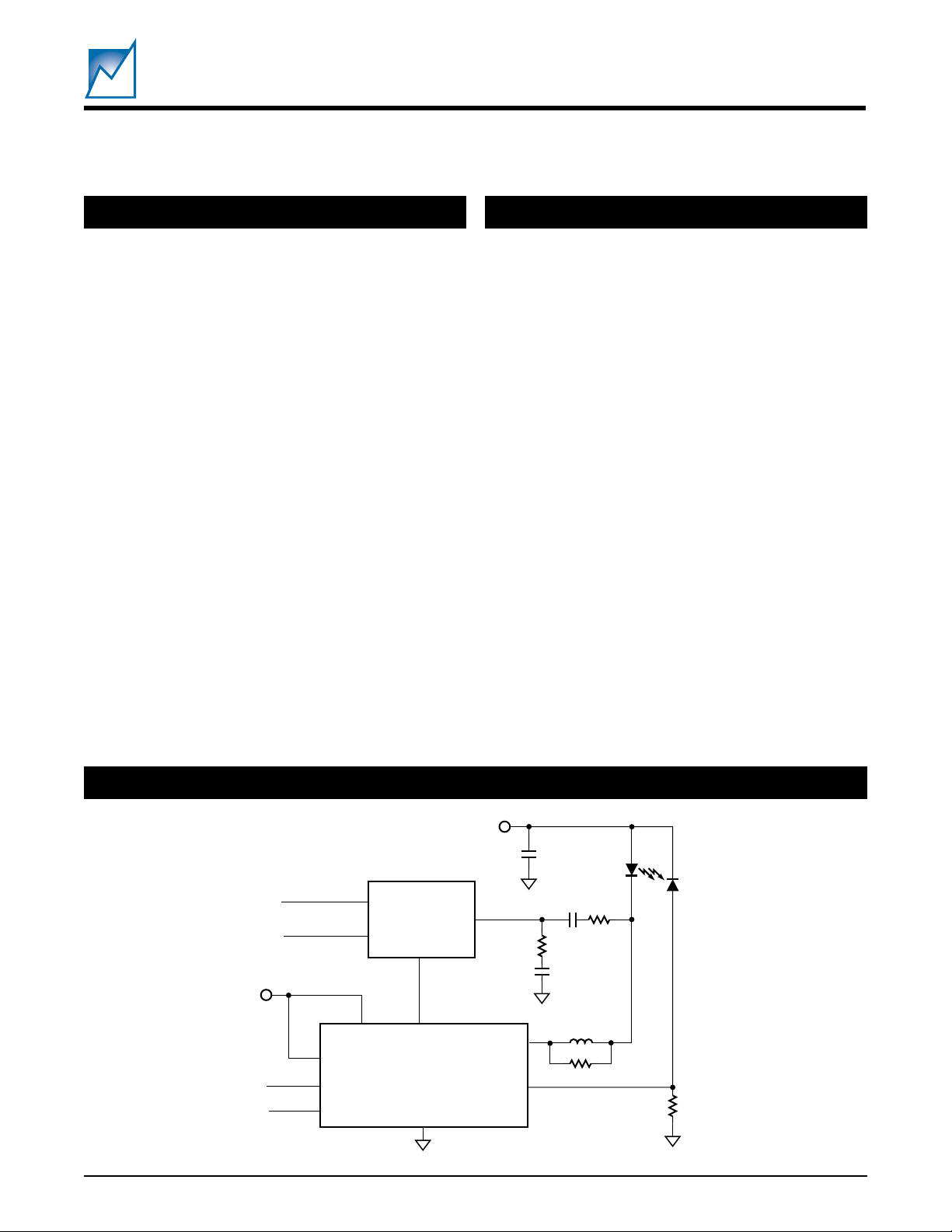
SIMPLIFIED APPLICATION DIAGRAM
V
DD
LASER
IN+
IN–
V
DD
V
AUTOMON
Interface
©SUMMIT MICROELECTRONICS, Inc., 2001 • 300 Orchard City Dr., Suite 131 • Campbell, CA 95008 • Phone 408-378-6461 • FAX 408-378-6586 • www.summitmicro.com
Characteristics subject to change without notice
SDA
SCL
LASER
MODULATION
DRIVER
MODN
DD
SML2108
IMOD
MODSET
BIASN
DETECT
V
SS
2053 3.0 10/03/01
DIODE
MONITOR
DIODE
2053 SAD
1
Page 2
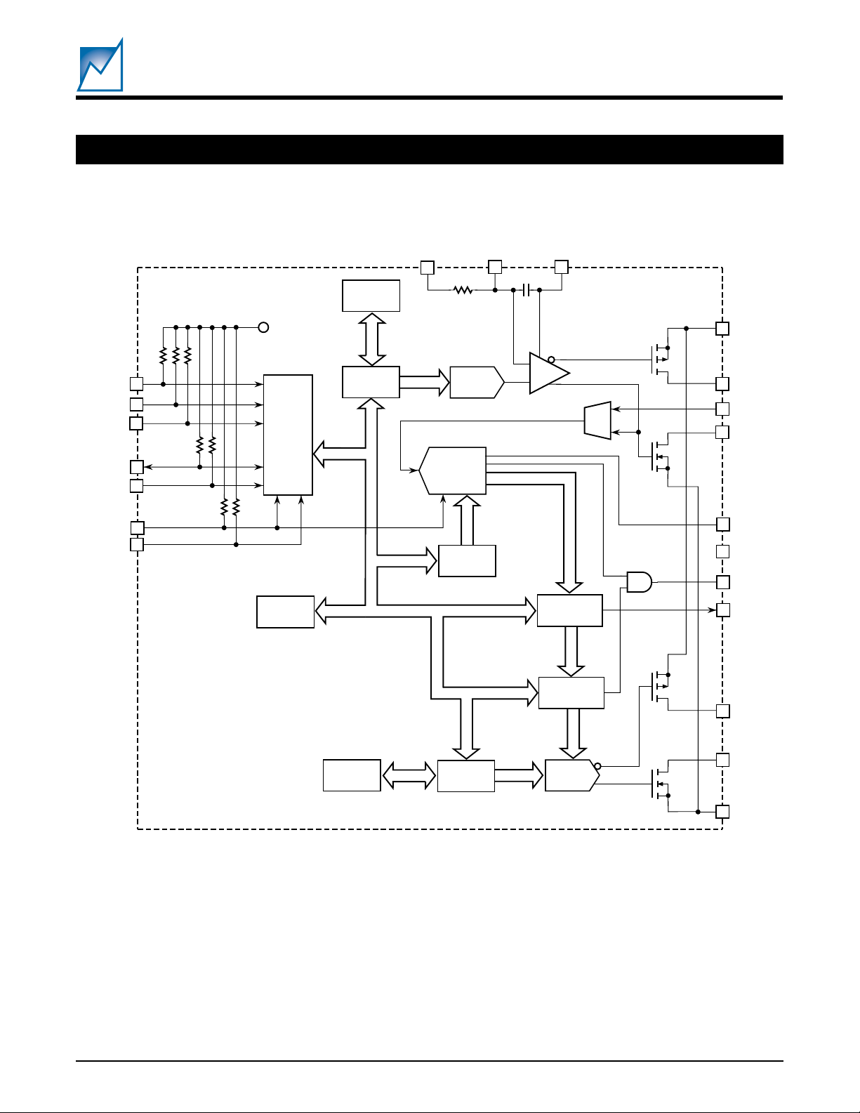
FUNCTIONAL BLOCK DIAGRAM
SML2108
PRELIMINARY
A0
A2
SDA
SCL
AUTOMON
CE#
A1
48
1
2
3
4
5
(All Rs 100kΩ)
6
V
CC
Config
10-Bit
NV Reg
10-Bit
DAC Reg
DETECT
12
10-Bit
DAC
8-Bit
ADC
NV Scaling
& Offset
CAP1
11
CAP2
10
–
+
ADC Read &
Alarm Reg
BIAS P
EXT TEMP
5
BIAS N
13
VSS A
14
VSS D
7
RDY
ALERT#
8
V
DD
NV Look-up
Table
8-Bit
NV Reg
2
2053 3.0 10/03/01
8-Bit
DAC Reg
8-Bit
DAC
2053 BD 2.2
SUMMIT MICROELECTRONICS, Inc.
MOD P
MOD N
V
SS
Page 3

PIN CONFIGURATION
SML2108
PRELIMINARY
48-Pin TQFP
A0
A1
A2
SDA
SCL
AUTOMON
RDY#
ALERT#
EXT TEMP
CAP2
CAP1
DETECT
CE#
VDDVDDVDDBIASP
BIASP
MODP
MODP
4847464544434241403938
1
2
3
4
5
6
7
8
9
10
11
12
1314151617181920212223
A
D
DDVDD
SS
SS
V
V
V
BIASP
BIASP
MODP
MODP
VDDVDDVSSV
DDVDD
VSSV
V
SS
37
36
35
34
33
32
31
30
29
28
27
26
25
24
SS
MODN
MODN
BIASN
BIASN
V
SS
V
SS
V
SS
V
SS
BIASN
BIASN
MODN
MODN
2053 PCon 2.1
PIN DESCRIPTIONS
DETECT (12)
This is the analog input from the laser monitor photodiode
for the integrator circuit. There is an on-board resistance
of 2MΩ between the DETECT input and CAP1 pin.
CAP1 and CAP2 (11 & 10)
Capacitor inputs for an external capacitor in the feedback
loop of the Mean Power Control Integrator. There is an onboard capacitance of 500pF.
AUTOMON (6)
Active high input used to enable the internal auto-monitor
function, which provides automatic adjustments to the
modulation output currents (MODP and MODN) based on
the internal A/D output and the values stored in the
nonvolatile lookup table. This pin has an internal 100kΩ
pull-up.
SUMMIT MICROELECTRONICS, Inc.
2053 3.0 10/03/01
ALERT# (8)
Active low, open-drain output. This pin is driven low
whenever the bias current increases beyond a predefined
nonvolatile threshold. This can be used to predict laser
failure.
SDA, SCL (4 & 5)
Data and Clock lines, respectively, whose function and
use are based on the industry standard I2C interface.
Lookup table values, configuration data, and D/A and A/D
registers may all be accessed via these two pins of the
SML2108. These pins have internal 100kΩ pull-ups.
A0, A1, A2 (1, 2, & 3)
Address Pins for the interface provided to allow multiple
devices on a single bus. These pins have internal 100kΩ
pull-ups.
3
Page 4

SML2108
PRELIMINARY
RDY# (7)
Active low, open-drain output. This pin is driven low
whenever the internal A/D is performing a conversion, or
while the on-board EEPROM is being programmed.
EXT TEMP (9)
Temperature input (or no connection). This pin can be
programmed as an input to the ADC and can interface a
temperature sensor. The EXT TEMP pin is multiplexed
with the bias current to provide a means of configuring the
input to the ADC. When EXT TEMP is programmed as the
input to the ADC using bit 5 of Register 1, the converted
value of the current entering this pin is used as the
address of the EEPROM lookup table. In this configuration the modulation current can be controlled by temperature rather than the bias current. Refer to the application
example on using the EXT TEMP pin. If this option is not
used the pin should be left floating.
V
A, VSSD (13 & 14)
SS
Analog and digital low-side supplies for on-board circuitry. Must be at same potential as all other VSS pins.
V
(15, 16, 21, 22, 39, 40, 45, 46, & 47)
DD
High-side supply for the Bias and Modulation currents and
power supply input for the chip.
(23, 24, 29, 30, 31, 32, 37, & 38)
V
SS
Power supply return.
CE# (48)
The chip enable input is active low and provides an
additional method of enabling the serial interface. The
state of this pin has no effect on the auto-monitor function.
This pin has an internal 100kΩ pull-up.
BIASP (17, 18, 43, & 44)
High-side mean bias control current. Current source
output range is programmable, with the optional ranges of
0 to 100mA or 0 to 10mA.
BIASN (27, 28, 33, & 34)
Low-side mean bias control current. Current sink input
range is 0 to 100mA.
MODP (19, 20, 41, &42)
High-side modulation control current. Current source
output range is programmable, with optional ranges of 0 to
100mA or 0 to 10mA.
MODN (25, 26, 35, &36)
Low-side modulation control current. Current sink input
range is 0 to 100mA.
4
2053 3.0 10/03/01
SUMMIT MICROELECTRONICS, Inc.
Page 5
ABSOLUTE MAXIMUM RATINGS*
SML2108
PRELIMINARY
Temperature Under Bias ...................... –55°C to 125°C
Storage Temperature ........................... –65°C to 150°C
Lead Solder Temperature (10 secs) ................... 300 °C
*COMMENT
Stresses listed under Absolute Maximum Ratings may cause permanent damage to the device. These are stress ratings only, and
functional operation of the device at these or any other conditions
outside those listed in the operational sections of this specification is not
implied. Exposure to any absolute maximum rating for extended
periods may affect device performance and reliability.
ELECTRICAL TABLES
(Over Recommended Operating Conditions; Voltages are relative to GND)
lobmySretemaraPsnoitidnoC.niM.pyT.xaMstinU
ecnamrofrePCDAlacipyT
º
N/SoitaresioNotlangiST
DHTnoitrotsidcinomrahlatoT08– Bd
noitaludomretnicinomrahkaeP
noitrotsid
ycaruccACD
noituloseR8stiB
gnissimonhcihwrofnoituloeR
deetnaraugerasedoc
ycaruccaevitaleR ½±BSL
LND 1±BSL
rorreelacsllufevitisoP2±BSL
V
rorretesfforalopinU
V
º
Cº52= 07Bd
A
redrOdn208– Bd
redrOdr308– Bd
8stiB
V5=2±BSL
SS
SS
V6.3
otV7.2=
2±BSL
2053 Elect Table A
SUMMIT MICROELECTRONICS, Inc.
RECOMMENDED OPERATING CONDITIONS
Temperature –40ºC to 85ºC.
Voltage 3.0V to 5.5V
2053 3.0 10/03/01
5
Page 6
ELECTRICAL TABLES (Continued)
lobmySretemaraPsnoitidnoC.niM.pyT.xaMstinU
V
DD
I
D
I
OL
I
IL
V
LO
V
HO
V
LI
V
HI
f
TNI
t
SUP
emit
TCETEDCDAottupniTCETED05.1V
I
PMETTXE
I
NDOM
I
PDOM
I
NSAIB
I
PSAIB
V
CAD
tnerruc
tnerruc
TRELAtuptuoTRELA
egatlovylppuS
tnerrucylppuS
tnerrucegakaeltupnIV
NI
tnerrucegakaeltuptuOV
egatlovwoltuptuOI
egatlovhgihtuptuO
LO
V
DD
V
DD
egatlovwoltupnI1.0– 3.0 × V
egatlovhgihtupnI7.0 × V
poolrotargetnI
ycneuqerf
noitazilibatspurewoP
stupnIgolanA
tupnitnerrucelacslluF 6.093Aµ
stuptuOgolanA
noitaludomlennahc-N
noitaludomlennahc-P
tnerrucsaiblennahc-N0001– Am
tnerrucsaiblennahc-P0001Am
tuptuoCADtiB-0105.1V
stuptuOlatigiD
SML2108
PRELIMINARY
noitaludomdnasaibmumixaM
tnerruc
-tuotnerrucnoitaludomdnasaiB
nepostup
VotV0=
DD
TUO
VotV0=
DD
Am2=4.0V
I,V5=
LO
I,V5.4<
LO
Aµ004–=4.2V
Aµ001–=V
sselsitnatsnocemitrotargetnI
sm01naht
situptuoTRELAniardnepO
evitca
35.5V
2Am
1Aµ
01Aµ
2.0– V
DD
V
DD
DD
5.0V
1zHk
01sm
0001– Am
0001Am
5Am
2053 Elect Table B
6
2053 3.0 10/03/01
SUMMIT MICROELECTRONICS, Inc.
Page 7
DEVICE OPERATION
SML2108
PRELIMINARY
General Description
The SML2108 is an adaptive power controller for laser
diodes with an active feedback loop used to calibrate and
control the mean and modulation power of high speed,
high power laser diodes. Inherent manufacturing tolerances introduce variations of performance in laser diodes.
These variations, combined with parametric changes over
the laser’s extreme temperature range and laser aging,
call for an efficient compensation solution. The SML2108,
with a minimum number of external components, is designed to compensate for these tolerances using a digital
control loop and a programmable nonvolatile calibration
lookup table.
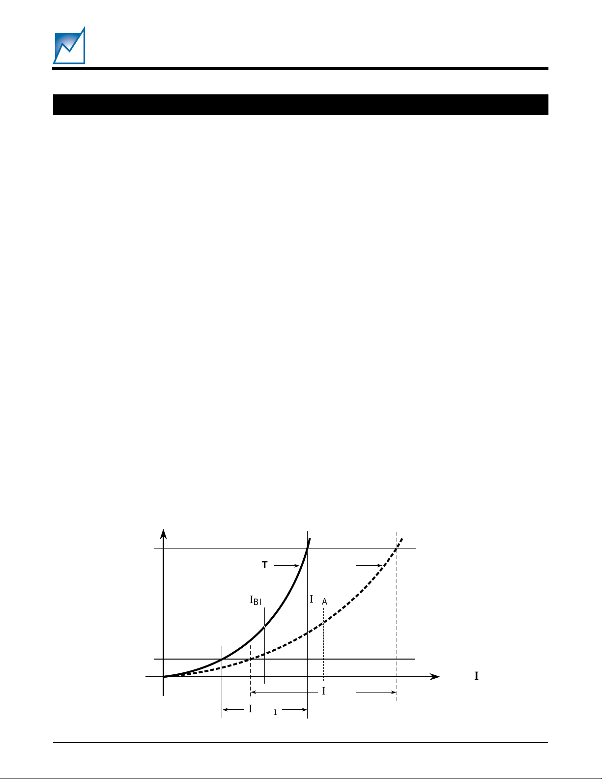
Figure 1 illustrates the usefulness of the SML2108. The
figure shows the output light power of a laser diode versus
its operating current. Depicted in the graph are typical
laser diode characteristics at two different temperatures.
At the first temperature (T
), the laser requires an average
1
bias current of IBIAS1. The modulation current needed to
switch the laser between its on and off state is labeled
IMOD1. The ratio of light power of its on state divided by
the light power of its off state is referred to as the extinction
ratio. Ideally the laser will maintain a constant extinction
ratio over its entire operating temperature range, as the
receiver module is calibrated to this level. Running the
laser driver at a higher extinction ratio indicates that power
is being wasted, whereas operating at a lower extinction
ratio indicates that data may possibly be lost.
The required bias current increases to IBIAS
when the
2
laser is operated at a second temperature (T2). The laser
requires a modulation of IMOD2 to maintain a constant
extinction ratio as in the T1 curve. The SML2108 is the
industry’s first integrated device capable of providing a
variable modulation current based on a function of either
the bias current or an external temperature. This ability
to compensate the modulation output current enables the
system designer to optimize the extinction ratio of the
laser driver module.
The SML2108 has been specified to remove the need for
any manual calibration of the laser control circuit. All
calibration values are programmed through an industry
standard 2-wire communication interface, whose protocol
and function can be controlled by most production ATE
equipment.
Bias Current — Mean Power Control
The SML2108 bias current output (BIASP or BIASN)
establishes the average power being delivered to an
external laser diode. The output of the laser diode is
separately monitored using a local back-face diode, the
output of which is tied to the DETECT pin of the SML2108.
This feedback loop becomes the mean power control for
the laser diode when coupled with the internal integrator.
The output block of the mean power control is shown in
Figure 2.
(On) 1
(Off) 0
Figure 1. Laser Current Increase Caused by Temperature Increase, Constant Light Power Out
SUMMIT MICROELECTRONICS, Inc.
Light
Power
I
BIAS
I
MOD
T1
I
1
1
2053 3.0 10/03/01
BIAS
I
MOD
T2
2
Total
2
2053 Fig01
I
7
Page 8

SML2108
PRELIMINARY
The built-in integration time constant is nominally 1ms.
This is accomplished by using an internal 2MΩ resistor
and 500pF capacitor. The time constant can be modified
by adding external capacitance between the CAP1 and
CAP2 terminals, and/or by adding external resistance
between the DETECT and CAP1 terminals. For stability
reasons it is not recommended that the time constant be
decreased to less than 100us.
The output of an internal 10-Bit DAC biases the positive
terminal of the integrating amplifier. This DAC provides an
analog reference to the integrator which is useful for initial
calibration of the laser module. The full-scale value of the
DAC output is 1.5V.
10-Bit Bias Control D/A
The 10-Bit D/A determines the reference voltage of the
non-inverting terminal of the integrating amplifier in the
mean power control loop. Associated with this DAC are a
10-Bit volatile register and a 10-Bit nonvolatile (NV) register. The content of the volatile register determines the
DAC output voltage. The DAC output voltage is given by
the following relation:
=×
V
DD
I
Source
BIAS
0 to 10 mA or
0 to 100 mA
ADC
Input
From MPC
Integrator
BIAS
CONTROL
BIASP
BIASN
I
Sink
BIAS
0 to 100 mA
2053 Fig02
Figure 2. Output Block 1: Mean Power Control
V
DD
I
Source
MOD
0 to 10 mA or
0 to 100 mA
where X = the decimal equivalent of the 10-Bit data stored
in the volatile register. Note that the DAC output voltage
is not directly accessible external to the chip. However,
when the SML2108 is placed in a typical application circuit,
the mean power control feedback loop forces the voltage
at the DETECT pin to be the same as the DAC output. On
device power-up the volatile register may be loaded with
all zeroes, or it may be loaded from the contents of the 10Bit nonvolatile register.
Access to the 10-Bit volatile register is obtained via the 2wire interface at slave address 1001
, word address 0.
BIN
Refer to Figures 9, 10, 12, and 13 for details on programming and reading data from the 10-Bit register. When
writing to the volatile register the new DAC output will
become valid immediately at the end of the write command. Reading the volatile register has no effect on the
DAC output. Reading or writing the volatile register has no
effect on the contents of the nonvolatile register.
The 10-Bit NV register can only be accessed indirectly
through the volatile register. The command sequence to
communicate with the NV register is the same as that of
the volatile register, except word address 2 is used instead
of 0. When reading the NV register, the data is first
MODP
From I
DAC
MOD
Figure 3. Output Block 2: I
MOD
CONTROL
MODN
Sink
I
MOD
0 to 100 mA
2053 Fig03
MOD
transferred into the volatile register where it may be
accessed by the serial interface. Note that upon this
transfer the DAC output will change immediately to reflect
the new data. Similarly, when writing to the NV register,
the data is first placed in the volatile register. At the
conclusion of the write command an internal nonvolatile
write sequence initiates the storage of the volatile contents
into the NV register.
8
2053 3.0 10/03/01
SUMMIT MICROELECTRONICS, Inc.
Page 9

SML2108
PRELIMINARY
Note that when modifying the 10-Bit DAC output, the mean
power control loop will become temporarily disrupted. It
may be several milliseconds before the bias current has
settled to its steady state value. Until then its value will be
undefined.
Modulation Current — Auto-Monitor Control
The laser bias current, which relates directly to laser
temperature, can be monitored using an internal currentsensing A/D converter. In the auto-monitor mode the 8Bit output of the converter is used as an address to the
EEPROM lookup table. The subsequent 8-Bit data output
from the lookup table becomes the input for the compensation DAC. The 8-Bit compensation DAC output is a
current in the range of 0 to 100mA and is used to control
the modulation current MODP and MODN. The output
block of the modulation current control is shown in Figure
3.
The lookup table provides an arbitrary mapping from bias
current to modulation current. The input range to the ADC
may be scaled and/or offset to provide maximum resolution within the appropriate conversion space. The sample
interval is programmable from 10µs to 1s. Refer to the
ADC section for further details about configuring the A/D.
The interface is used to program the configuration registers as well as lookup table values.
Lookup Table
A 2k-Bit (256 x 8) memory array of internal EEPROM
comprises the internal lookup table. This array is accessed via the 2-wire serial interface using a slave address of 1010
this may be set to 1110
. (Note: 1010
BIN
is the default, however
BIN
, depending upon the contents
BIN
of Configuration Register 2.) Refer to the Bus Interface
section for details on programming and reading data from
the device.
In the auto-monitor mode the content of the array represents the transfer function between the A/D output and the
final value of modulation current. Using a lookup table to
implement this function allows arbitrary functions, and
even nonlinear relations, to be easily realized. Also, the
use of a lookup table allows each device to be customized
to normalize overall module operation.
Although the memory may normally be read and written as
a standard memory, a security feature exists in the configuration settings that will prevent any external access to
the array. Additionally, if the auto-monitor feature is not
used, then the modulation output current may be programmed to a fixed value, and the array may be used as
a standard memory to store device settings, board
identification values, production dates, etc.
8-Bit Current Sensing A/D
Though the internal ADC is normally used during the AutoMonitor mode, a conversion may also be performed on
2
command via the I
C interface. Figure 25 shows the
details for forcing a manual A/D conversion and readout.
Access to the ADC is obtained using slave address
1001
, word address 8. Notice there is a delay of t
BIN
ADC
required while the Acknowledge clock is high preceding
the data byte.
8-Bit Current Output D/A
The 8-Bit D/A defines the modulation output current.
Associated with this DAC are an 8-Bit volatile register and
an 8-Bit nonvolatile (NV) register. The content of the
volatile register determines the DAC output current. The
DAC output current is given by the following relation:
=×
where X = the 8-Bit data stored in the volatile register. On
device power-up the volatile register may be loaded with
all zeroes or it may be loaded from the contents of the 8Bit nonvolatile register.
Access to the 8-Bit volatile register is obtained via the 2wire interface at slave address 1001
, word address 4.
BIN
Refer to Figures 8 and 11 for details on programming and
reading data from the 8-Bit register. When writing to the
volatile register, the new DAC output will become valid
immediately at the end of the write command. Reading the
volatile register has no effect on the DAC output. Reading
or writing the volatile register has no effect on the contents
of the nonvolatile register.
The 8-Bit NV register can only be accessed indirectly
through the volatile register. The command sequence to
communicate with the NV register is the same as that of
the volatile register, except word address 6 is used instead
of 4. When reading the NV register the data is first
transferred into the volatile register where it may be
accessed by the serial interface. Note that upon this
transfer the DAC output will change immediately to reflect
the new data. Similarly, when writing to the NV register,
the data is first placed in the volatile register. At the
conclusion of the write command, an internal nonvolatile
write sequence initiates the storage of the volatile contents
into the NV register.
SUMMIT MICROELECTRONICS, Inc.
2053 3.0 10/03/01
9
Page 10

ADC SCALING AND OFFSET
SML2108
PRELIMINARY
The ADC can be customized to monitor a particular range
of bias current by programming Register 0. Bits 3 and 2
control the scaling of the ADC while bits 1 and 0 control the
ADC offset. The four graphs (Figures 4, 5, 6, & 7) illustrate
the ADC scale values, according to the two bit code. In
each Graph the curves are differentiated by the ADC offset
values. Note: if using I
with the maximum current
BIASP
option set to 10 mA, divide the x-axis value by 10 (i.e., 75
= 7.5, etc.).
255
224
192
160
128
96
ADC OUTPUT
64
Offset
00
01
10
11
These combinations of scales and offsets allow the resolution to be maximized over a given range of current. For
example, if the bias current is known to be in the range of
30mA to 70mA the choice would be the Half scale graph
(code 10
) and the ¼ offset curve (code 01
BIN
BIN
) to
maximize the resolution of the ADC.
Note that these graphs assume a full scale bias current of
100mA. When the ADC is configured to receive input from
the EXT TEMP pin full scale current becomes 390.6µA,
which limits the internal 1/256 scale factor between bias
current and the ADC input current.
255
224
192
160
128
ADC OUTPUT
Offset
00
01
10
11
96
64
32
0
0
10
255
224
192
160
128
96
ADC OUTPUT
64
32
0
0
10
32
0
50
20
30
20
30
40
I
BIAS
00
01
10
11
40
I
BIAS
Offset
50
(mA)
(mA)
60
70
) with Offset
BIN
60
70
100
80
90
2053 Fig04
Figure 5. Half Scale (code 10
100
80
90
2053 Fig06
0
10
255
224
192
160
128
96
ADC OUTPUT
64
32
0
0
10
50
I
BIAS
I
BIAS
(mA)
50
(mA)
60
70
) with OffsetFigure 4. Full Scale (code 11
BIN
60
70
20
30
40
Offset
00
01
10
11
20
30
40
100
80
90
2053 Fig05
100
80
90
2053 Fig07
Figure 6. Quarter Scale (code 01
10
) with Offset Figure 7. Tenth Scale (code 00
BIN
2053 3.0 10/03/01
) with Offset
BIN
SUMMIT MICROELECTRONICS, Inc.
Page 11

REGISTERS
SML2108
PRELIMINARY
REGISTER BIT MAPS
The SML2108 has three user programmable, nonvolatile
configuration registers. These registers decide which
features are enabled and determine some characteristics
of the part functions. Reading and writing to these
registers is accomplished via the I2C interface, as shown
in Figures 26 and 27. A description of the registers
follows.
Register 0
This register is used to configure the 8-Bit ADC that
monitors the bias current. Bit 7 enables the ADC alert to
be latched, which will hold the ALERT pin low until the alert
is reset. Bits 6, 5, and 4 are used to set the sample interval
of the ADC. The input to the ADC can be scaled and offset
to provide maximum resolution over the bias current. Bits
3 and 2 are used to set the full scale range of the ADC,
while bits 1 and 0 are used to set the ADC offset. See the
Table.
Register 1
This register controls multiple functions. Bit 7 disables the
alert during a manual analog-to-digital conversion of the
bias current. Bit 6 selects the action that will reset an alert
from the ADC. When this bit is set to a 0 any device read
or write will reset the alert. When set to a 1 the alert will be
reset by a low AUTOMON signal. Bit 5 is used to toggle
the source of the ADC input between the I
current and
BIAS
the EXT TEMP signal. Bit 2 initializes the input of the 10
bit DAC to either zero or a stored value from a nonvolatile
register when the device is powered up. Bit 1 initializes the
input of the 8 bit DAC to either zero or a stored value from
a nonvolatile register when the device is powered up. Bit
0 sets the maximum P-channel bias current (I
modulation current (I
) to either 10mA or 100mA.
MODP
BIASP
) and
Register 2
This register controls several functions related to the bus
interface. Bits 7 and 6 control the read and write access
to the configuration registers. It is imperative that register
2 be programmed properly to prevent an inadvertent
lockout. Bit 5 determines whether the memory array is
76543210
CDA
trelA
0
1
xxx
lavretnIelpmaSCDAegnaRCDAtesffOCDA
000
001
010
011
100
101
xx
xx
110
x
111
00
01
10
xxx
11
xx
00
01
10
11
Register 0
noitcnuF
dehctaltontrelA
dehctaltrelA
lavretnielpmassµ5.8
sµ43""
sµ272""
""sm81.2
sm6""
sm42""
sm291""
s45.1""
tnerrucsaibelacslluf01/1
tnerrucsaibelacslluf4/1
tnerrucsaibelacslluf2/1
tnerrucsaibelacslluF
tesffooN
tesffotnerrucsaibelacslluffo4/1
tesffotnerrucsaibelacslluffo2/1
tesffotnerrucsaibelacslluffo4/3
2053 Reg0
SUMMIT MICROELECTRONICS, Inc.
2053 3.0 10/03/01
11
Page 12

SML2108
PRELIMINARY
available or locked. Bit 4 selects the device type address
for accessing the memory array, while bit 3 determines
whether the device must receive a bus address that
corresponds to the biasing of the address pins. Bit 2 is
used to enable an alert condition on the ADC to shut down
the bias current. Bits 1 & 0 are unused.
76543210
trelA
0
trelA
x
1
CDA
teseR
tupnI
desunU
tiB-01
CAD
tiB-8
I
CAD
x
0
1
0
x
x
1
xx
x
0
1
x
x
x
0
1
x
Register 1
noitcnuF
PSAIB
noisrevnoclaunamgniruddewollatontrelA
noisrevnoclaunamgniruddewollatrelA
etirWrodaeRybtesertrelA
nipNOMOTUAnowoLybtesertrelA
I
Iro
NSAIB
PSAIB
x
CDAottupnitnerruc
CDAottupninipPMETTXE
purewopnoorezsiCADottupnI
noretsigerelitalovnonmorfsiCADottupnI
purewop
purewopnoorezsiCADottupnI
noretsigerelitalovnonmorfsiCADottupnI
purewop
0
1
:Am001sitnerrucxaMI
I:Am01sitnerrucxaM
I,
PSAIB
PDOM
I,
PSAIB
PDOM
2053 Reg1 1.0
76 5 4 3210
sseccAretsigeR
yromeM
sseccA
eciveD
sserddA
niP
sserddA
trelA
noitcA
0x
10
11
x
x
0
1
x
x
0
xx
xx
1
0
x
1
x
0
x
1
Register 2
12
2053 3.0 10/03/01
desunU
noitcnuF
etirWrodaeRon;dekcolsretsigeRllA
etirWon;sretsigeRlladaeR
sretsigeRllaetirWdnadaeR
elbaliavayarrayromeM
etirWrodaeRon;dekcolyarrayromeM
0101sisserddA
NIB
0111sisserddA
NIB
desaibnipsserddaotsdnopseR
ylnosserdda
sserddasubynaotsdnopseR
trelaybdetceffanutnerrucsaiB
noitidnoc
tnerrucsaibnwodstuhsnoitidnoctrelA
2053 Reg2 1.0
SUMMIT MICROELECTRONICS, Inc.
Page 13

BUS INTERFACE
GENERAL DESCRIPTION
SML2108
PRELIMINARY
The I2C bus is a two-way, two-line serial communication
between different integrated circuits. The two lines are:
a serial Data line (SDA) and a serial Clock line (SCL). All
Summit Microelectronics parts support a 100kHz clock
rate, and some support the alternative 400kHz clock.
Check the AC Electrical Table for the value of f
t
SCL
SDA In
SDA Out
R
t
SU:SDA
t
AA
t
HD:SDA
t
F
SCL
. The
t
HIGH
t
HD:DAT
Figure 8. I
lobmySretemaraPsnoitidnoC.niM.xaMstinU
SDA line must be connected to a positive supply by a pullup resistor located on the bus. Summit parts have a
Schmitt input on both lines. See Figure 8 and Table 1 for
waveforms and timing on the bus. One bit of Data is
transferred during each Clock pulse. The Data must
remain stable when the Clock is high.
t
LOW
t
SU:DAT
t
DH
2
C Data Timing
t
SU:STO
t
BUF
2053 Fig08
f
LCS
t
WOL
t
HGIH
t
FUB
t
ATS:US
t
ATS:DH
t
OTS:US
t
AA
t
HD
t
R
t
F
t
TAD:US
t
TAD:DH
ycneuqerfkcolcLCS 0001zHk
doirepwolkcolC 7.4sµ
doirephgihkcolC 0.4sµ
)1(emiteerfsuBnoissimsnartwenerofeB7.4sµ
emitputesnoitidnoctratS 7.4sµ
emitdlohnoitidnoctratS 0.4sµ
emitputesnoitidnocpotS 7.4sµ
tuptuodilavotegdekcolC)nelcyc(ADSdilavotwolLCS3.05.3sµ
)1(emitdlohtuOataDegnahcADSot)1+nelcyc(wolLCS3.0sµ
)1(emitesirADSdnaLCS 0001sn
)1(emitllafADSdnaLCS 003sn
)1(emitputesnIataD 052sn
)1(emitdlohnIataD 0sn
IT)1(ADSdnaLCSretlifesioNnoisserppusesioN001sn
t
RW
t
CDA
emitelcycetirW 5sm
kcolcdednetxeCDA 02sµ
Note (1) These values are guaranteed by design.
SUMMIT MICROELECTRONICS, Inc.
Table 1. I2C Data Timing
2053 3.0 10/03/01
2053 Table01 2.1
13
Page 14

SML2108
PRELIMINARY
Start and Stop Conditions
Both Data and Clock lines remain high when the bus is not
busy. Data transfer between devices may be initiated with
a Start condition only when SCL and SDA are high. A highto-low transition of the Data line while the Clock line is high
is defined as a Start condition. A low-to-high transition of
the Data line while the Clock line is high is defined as a Stop
condition. See Figure 9.
SCL
SDA In
START
Condition
Figure 9. I
2
C Start and Stop Timing
STOP
Condition
2053 Fig09
Protocol
The protocol defines any device that sends data onto the
bus as a Transmitter, and any device that receives data
as a Receiver. The device controlling data transmission
is called the Master, and the controlled device is called
the Slave. In all cases the Summit Microelectronic
devices are Slave devices, since they never initiate any
data transfers.
Acknowledge
Data is always transferred in 8-Bit bytes. Acknowledge
(ACK) is used to indicate a successful data transfer. The
Transmitting device will release the bus after transmitting
eight bits. During the ninth clock cycle the Receiver will
pull the SDA line low to Acknowledge that it received the
eight bits of data (See Figure 10). The termination of a
Master Read sequence is indicated by a non-Acknowledge (NACK), where the Master will leave the Data line
high.
SCL
SDA
Trans
SDA
Rec
1
2
3
8
9
ACK
2053 Fig10
Figure 10. Acknowledge Timing
Read and Write
The first byte from a Master is always made up of a seven
bit Slave address and the Read/Write bit. The R/W bit tells
the Slave whether the Master is reading Data from the bus
or writing Data to the bus (1 = Read, 0 = Write). The first
four of the seven address bits are called the Device Type
Identifier (DTI).
In the Read mode the SML2108 transmits eight bits of
data, then releases the SDA line, and monitors the line for
an Acknowledge signal. If an Acknowledge is detected,
and no Stop condition is generated by the Master, the
SML2108 will continue to transmit data. If an Acknowledge is not detected (NACK) the SML2108 will terminate
further data transmission. See Figure 12.
In the Write mode the SML2108 receives eight bits of data,
then generates an Acknowledge signal. It will continue to
generate ACKs until a Stop condition is generated by the
Master. This will indicate to the Summit part that it should
begin its internal nonvolatile Write cycle. See Figure 13.
SCL
SDA
14
1
1
2
0
3
1
4
0
5
x
6
x
7
x
8
R/W
9
ACK
2053 Fig11
Figure 11. Typical Master Address Byte Transmission
2053 3.0 10/03/01
SUMMIT MICROELECTRONICS, Inc.
Page 15

SML2108
PRELIMINARY
Master
SDA
Slave
Master
SDA
Slave
S
T
A
R
T
0
1
0
1
xx
R
/
W
xxxxxxx
x
R
A
C
K
A
C
K
xx xx
2053 Fig12
S
N
T
A
C
K
Optional
O
P
Figure 12. Read
S
T
A
R
T
0
1
0
1
xx
R
/
W
x
xxxxxxxx
W
A
C
K
xx xx
A
C
K
2053 Fig13
S
T
O
P
A
C
K
Figure 13. Write
Random Address Read
Random address Read operations allow the Master to
access any memory location in a random fashion. This
operation involves a two-step process. First, the Master
issues a Write command which includes the Start condition and the Slave address field (with the R/W bit set to
Write) followed by the address of the word it is to read.
This procedure sets the internal address counter of the
SML2108 to the desired address. After the word address
Acknowledge is received by the Master, it immediately
reissues a Start condition followed by another Slave
address field with the R/W bit set to Read. The SML2108
will respond with an Acknowledge and then transmit the
8 data bits stored at the addressed location. At this point,
the Master does not Acknowledge the transmission, but
does generate a Stop condition. The SML2108 discontinues data transmission.
Sequential Read
Sequential Reads can be initiated as either a current
address Read or a random access Read. The first word
is transmitted as with the other byte Read modes (current
address byte Read or random address byte Read).
However, the Master now responds with an Acknowledge, indicating that it requires additional data. The
SML2108 continues to output data for each Acknowledge
received. The Master terminates the sequential Read
operation by not responding with an Acknowledge, and
issues a Stop condition. During a sequential Read
operation the internal address counter is automatically
incremented with each Acknowledge signal. For Read
operations all address bits are incremented, allowing the
entire array to be read using a single Read command.
After a count of the last memory address the address
counter will ‘rollover’ and the memory will continue to
output data.
The protocol for reading and writing to the registers and
the lookup table are illustrated in Figures 14 through 24.
SUMMIT MICROELECTRONICS, Inc.
2053 3.0 10/03/01
15
Page 16

TIMING DIAGRAMS
SML2108
PRELIMINARY
Master
SDA
Slave
Master
SDA
Slave
S
T
A
R
T
1 0 1 0
Device
Address
x x x
Data
R/
W
A
C
K
Word Address
0
Byte
n
A
C
K
Data
Byte
n+1
A
C
K
Figure 14. Look-up Table Page/Byte Write
A
C
K
S
T
A
R
T
1 0 1 0
Device
Address
x x x
S
T
A
R
T
1 0 1 0
Device
Address
x x x
R/
W
0
Word Address
A
C
K
Figure 15. Look-up Table Random Address Read with Dummy Write
R/
W
A
C
K
2053 Fig14
2053 Fig15
S
T
O
P
S
N
T
A
O
C
P
K
Data
Byte
n+15
A
A
C
C
K
K
A
C
K
1
Data Byte
Master
SDA
Slave
S
T
A
R
T
1 0 1 0
Master
SDA
Slave
S
T
A
C
K
A
R
T
1 0 1 0
Device
Address
x x x
R/
W
1
A
C
K
Device
Address
x x x
R/
W
A
C
K
Word Address
0
Figure 16. Look-up Table Sequential Read with Dummy Write
S
T
A
R
T
1 0 0 1
Device
Address
x x x
R/
W
Location Address
0 0 0 0 0 1 0 0
0
A
C
K
D7D6D5D4D3D2D1D
A
C
K
Figure 17. 8-Bit DAC Volatile Register Write
First
Data
Byte
A
C
K
S
T
O
P
Data
C
Byte
K
Last
A
N
A
C
K
2053 Fig16
S
T
O
P
0
A
C
2053 Fig17
K
16
2053 3.0 10/03/01
SUMMIT MICROELECTRONICS, Inc.
Page 17

SML2108
PRELIMINARY
Master
SDA
Slave
S
T
A
R
T
1 0 0 1
Master
SDA
Slave
S
T
Device
Address
x x x
R/
W
Location Address
0 0 0 0 0 1 0 0
0
A
C
K
A
R
T
1 0 0 1
A
C
K
Device
Address
x x x
R/
W
D7D6D5D4D3D2D1D
1
A
C
K
Figure 18. 8-Bit DAC Volatile Register Read with Dummy Write
S
T
A
R
T
1 0 0 1
Device
Address
x x x
R/
W
Location Address
0 0 0 0 0 1 1 0
0
A
C
K
D7D6D5D4D3D2D1D
0
A
C
K
Figure 19. 8-Bit DAC Nonvolatile Register Write
A
C
K
S
T
O
P
2053 Fig19
N
A
C
K
0
2053 Fig18
S
T
O
P
Master
SDA
Slave
Master
SDA
Slave
S
T
A
R
T
1 0 0 1
S
T
A
R
T
S
T
Device
Address
x x x
R/
Location Address
W
0 0 0 0 0 1 1 0
0
A
C
K
A
R
T
1 0 0 1
A
C
K
Device
Address
x x x
R/
W
1
A
C
K
Figure 20. 8-Bit DAC Nonvolatile Register Read with Dummy Write
Device
Address
1 0 0 1
x x x
R/
W
Location Address
0 0 0 0 0 0 0 0
0
A
C
K
A
C
K
x x x
x x x
D9D
D7D6D5D4D3D2D1D
8
A
C
K
Figure 21. 10-Bit DAC Volatile Register Write
D7D6D5D4D3D2D1D
2053 Fig20
0
2053 Fig21
S
N
T
A
O
C
P
K
0
S
T
O
P
A
C
K
SUMMIT MICROELECTRONICS, Inc.
2053 3.0 10/03/01
17
Page 18

Master
SDA
1 0 0 1
Device
Address
x x x
R/
W
Location Address
0 0 0 0 0 0 1 0
0
x x x
x x x
D9D
D7D6D5D4D3D2D1D
8
SML2108
PRELIMINARY
S
T
O
P
0
Master
SDA
Slave
Master
SDA
Slave
Slave
S
T
A
R
T
S
T
A
R
T
1 0 0 1
1 0 0 1
A
C
K
A
C
K
A
C
K
Figure 22. 10-Bit DAC Nonvolatile Register Write
S
T
Device
Address
x x x
R/
Location Address
W
0 0 0 0 0 0 0 0
0
A
C
K
A
C
K
A
R
T
1 0 0 1
Device
Address
x x x
R/
W
x x x
x x x
1
A
C
K
Figure 23. 10-Bit DAC Volatile Register Read with Dummy Write
S
T
Device
Address
x x x
R/
Location Address
W
0 0 0 0 0 0 1 0
0
A
C
K
A
R
T
1 0 0 1
A
C
K
Device
Address
x x x
R/
W
x x x
x x x
1
A
C
K
A
C
K
D7D6D5D4D3D2D1D
D9D
8
A
C
K
D7D6D5D4D3D2D1D
D9D
8
A
C
K
2053 Fig22
2053 Fig23
2053 Fig24
S
N
T
A
O
C
P
K
0
S
N
T
A
O
C
P
K
0
Master
SDA
Slave
SCL
18
S
T
A
R
T
1 0 0 1
Figure 24. 10-Bit DAC Nonvolatile Register Read with Dummy Write
S
T
A
R
T
x x x
0 0 0 0 1 0 0 0
0
A
C
K
A
C
K
1 0 0 1
x x x
1
t
ADC
D7D6D5D4D3D2D1D
A
C
K
Figure 25. ADC Read
2053 3.0 10/03/01
SUMMIT MICROELECTRONICS, Inc.
N
A
C
K
0
2053 Fig25
S
T
O
P
Page 19

SML2108
PRELIMINARY
Master
SDA
Slave
Master
SDA
Slave
S
T
A
R
T
1 0 1 1
S
T
A
R
T
1 0 1 1
Device
Address
x x x
R/
W
0 0 0 0 0 0
0
A
C
K
Location Address
R
R
1
D7D6D5D4D3D2D1D
0
A
C
K
Figure 26. Configuration Register Write
S
T
Device
Address
x x x
R/
W
0 0 0 0 0 0
0
A
C
K
Location Address
A
R
T
R
R
1
0
1 0 0 1
A
C
K
Device
Address
x x x
R/
W
1
A
C
K
Figure 27. Configuration Register Read with Dummy Write
S
T
O
P
0
A
C
2053 Fig26
K
D7D6D5D4D3D2D1D
2053 Fig27
S
N
T
A
O
C
P
K
0
APPLICATIONS
APPLICATION EXAMPLE USING EXTERNAL
TEMPERATURE INPUT
The EXT TEMP pin of the SML2108 allows the input of the
internal ADC to be driven from an external device, rather
than a mirrored version of the bias current. Figure 28
shows an example using a National Semiconductor
LM334 to deliver a current into the SML2108 that is
proportional to absolute temperature. The scale and
offset features of the ADC input can be used to center this
current and maximize the full range of the look-up table.
For this application the current I
LM334 and into the EXT TEMP pin of the SML2108 is
given by the following equation:
I
= 227µV / oK / R
SET
SET
For example, using a value of 210Ω for R
current of 295µA at 0oC and 387µA at 85oC.
Next select scale and offset values of the ADC input that
will optimize the current range of the LM334. Nominal fullscale input current of the ADC is 390.6µA (= 100mA/256).
coming out of the
SET
yields a
SET
By setting the input offset to ¾ scale (293µA) and the fullscale range to ¼ scale (97.6µA), then the zero scale of the
internal ADC becomes 293µA, and the full-scale is
390.6µA. This represents a temperature range of approximately –2oC to 88
o
C using a 210Ω resistor in the configu-
ration shown. (These settings correspond to configuration
Register 0, Bits 3 - 0 set to 7
5V
LM334
+
–
R
210Ω ±1%
SET
HEX
I
SET
.)
SML2108
EXT TEMP
2053 Fig28
Figure 28. Example of an External Temperature
Sensing Device
SUMMIT MICROELECTRONICS, Inc.
2053 3.0 10/03/01
19
Page 20

PACKAGE
48 PIN TQFP PACKAGE
SML2108
PRELIMINARY
Pin 1
0.354
(9.00)
A
BSC
0.276
(7.00)
[A]
BSC
[B]
B
Ref. JEDEC MS-026
[A]
[B]
Inches
(Millimeters)
0.037 - 0.041
(0.95 - 1.05)
0.047
0.007 - 0.011
(0.17 - 0.27)
MAX
(1.2)
0.004 - 0.008
(0.09 - 0.20)
0.02
(0.5)
DETAIL "A"
DETAIL "B"
BSC
0.039
(1.00)
0.018 - 0.030
(0.45 - 0.75)
48 Pin TQFP
20
ORDERING INFORMATION
SML2108
F
Base Part Number
Also availabe in die form. Contact the factory.
2053 3.0 10/03/01
Package
F = 48 Pin TQFP
SUMMIT MICROELECTRONICS, Inc.
Page 21

PART MARKING
SUMMIT
.
SML2108 F
L YY WW
F = Package type (TQFP)
L
= Lot number
YY
= Year
WW
= Work Week
SML2108
PRELIMINARY
NOTICE
SUMMIT Microelectronics, Inc. reserves the right to make changes to the products contained in this publication in
order to improve design, performance or reliability. SUMMIT Microelectronics, Inc. assumes no responsibility for
the use of any circuits described herein, conveys no license under any patent or other right, and makes no
representation that the circuits are free of patent infringement. Charts and schedules contained herein reflect
representative operating parameters, and may vary depending upon a user’s specific application. While the
information in this publication has been carefully checked, SUMMIT Microelectronics, Inc. shall not be liable for any
damages arising as a result of any error or omission.
SUMMIT Microelectronics, Inc. does not recommend the use of any of its products in life support or aviation applications
where the failure or malfunction of the product can reasonably be expected to cause any failure of either system or to
significantly affect their safety or effectiveness. Products are not authorized for use in such applications unless
SUMMIT Microelectronics, Inc. receives written assurances, to its satisfaction, that: (a) the risk of injury or damage has
been minimized; (b) the user assumes all such risks; and (c) potential liability of SUMMIT Microelectronics, Inc. is
adequately protected under the circumstances.
Power Management for Communications™
This document supersedes all previous versions.
© Copyright 2001 SUMMIT Microelectronics, Inc.
I2C is a trademark of Philips Corporation.
SUMMIT MICROELECTRONICS, Inc.
2053 3.0 10/03/01
21
 Loading...