

Page 1
t
a(R)
(MAX)
t
a(SQ)
(MAX)
t
c(W)
(MIN)
SMJ55161-75
80 ns 25 ns 150 nsSMJ55161-80
75 ns 23 ns 140 ns
t
c(P)
(MIN)
t
c(SC)
(MIN)
I
CC1
(MAX)
I
CC1A
(MAX)
50 ns 30 ns 160 mA 195 mA
48 ns 24 ns 165 mA 210 mA
ROW ENABLE SERIAL DATA CYCLE TIME PAGE MODE CYCLE TIME
SERIAL PORT STAND-BYSERIAL PORT AC-
TIVE
ACCESS TIME ACCESS TIME DRAM DRAM SERIAL
OPERATING CURRENT OPERATING CURRENT
SMJ55161
262144 BY 16-BIT
MULTIPORT VIDEO RAM
SGMS056D – MA Y 1995 – REVISED OCT OBER 1997
1
POST OFFICE BOX 1443 • HOUSTON, TEXAS 77251–1443
D
Organization:
– DRAM: 262 144 by 16 Bits
– SAM: 256 by 16 Bits
D
Dual-Port Accessibility – Simultaneous and
Asynchronous Access From the DRAM and
SAM Ports
D
Data-Transfer Function From the DRAM to
the Serial-Data Register
D
(4 × 4) × 4 Block-Write Feature for Fast
Area-Fill Operations; as Many as Four
Memory-Address Locations Written Per
Cycle From the 16-Bit On-Chip Color
Register
D
Write-Per-Bit Feature for Selective Write to
Each RAM I/O; Two Write-Per-Bit Modes to
Simplify System Design
D
Byte-Write Control (CASL, CASU) Provides
Flexibility
D
Extended Data Output for Faster System
Cycle Time
D
Enhanced Page-Mode Operation for Faster
Access
D
CAS-Before-RAS (CBR) and
Hidden-Refresh Modes
D
Long Refresh Period
Every 8 ms (Maximum)
D
Up to 45-MHz Uninterrupted Serial-Data
Streams
D
256 Selectable Serial-Register Starting
Locations
D
SE-Controlled Register-Status QSF
D
Split-Register-Transfer Read for Simplified
Real-Time Register Load
D
Performance Ranges:
D
Programmable Split-Register Stop Point
D
3-State Serial Outputs Allow Easy
Multiplexing of Video-Data Streams
D
All Inputs/Outputs and Clocks TTL
Compatible
D
Compatible With JEDEC Standards
D
Designed to Work With the Texas
Instruments Graphics Family
TRG
SC
SE
V
SS
SQ15
DQ15
SQ14
DQ14
V
CC
SQ13
DQ13
SQ12
DQ12
V
SS
SQ11
DQ11
SQ10
DQ10
V
CC
SQ9
DQ9
SQ8
DQ8
DSF
V
SS
NC / GND
CASU
QSF
A0
A1
A2
A3
V
SS
V
CC
V
SS
SQ0
DQ0
SQ1
DQ1
V
CC
SQ2
DQ2
SQ3
DQ3
V
SS
SQ4
DQ4
SQ5
DQ5
V
CC
SQ6
DQ6
SQ7
DQ7
V
SS
CASL
WE
RAS
A8
A7
A6
A5
A4
V
CC
1
2
3
4
5
6
7
8
9
10
11
12
13
14
15
16
17
18
19
20
21
22
23
24
25
26
27
28
29
30
31
32
64
63
62
61
60
59
58
57
56
55
54
53
52
51
50
49
48
47
46
45
44
43
41
42
40
39
38
37
36
35
34
33
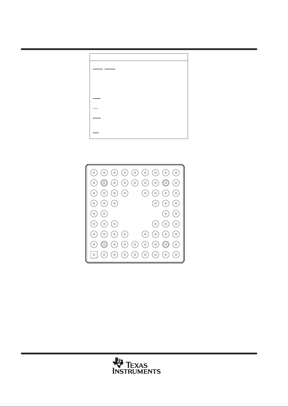
HKC PACKAGE
(TOP VIEW)
PRODUCTION DATA information is current as of publication date.
Products conform to specifications per the terms of Texas Instruments
standard warranty. Production processing does not necessarily include
testing of all parameters.
Copyright 1997, Texas Instruments Incorporated
Please be aware that an important notice concerning availability, standard warranty, and use in critical applications of
Texas Instruments semiconductor products and disclaimers thereto appears at the end of this data sheet.
Page 2
SMJ55161
262144 BY 16-BIT
MULTIPORT VIDEO RAM
SGMS056D – MA Y 1995 – REVISED OCT OBER 1997
2
POST OFFICE BOX 1443 • HOUSTON, TEXAS 77251–1443
98765432
J
H
G
F
E
D
C
B
A
1
GB PACKAGE
(BOTTOM VIEW)
PIN NOMENCLATURE
A0–A8 Address Inputs
CASL
, CASU Column-Address Strobe/Byte Selects
DQ0 –DQ15 DRAM Data I/O, Write Mask Data
DSF Special-Function Select
NC/GND No Connect/Ground (Important: Not
connected internally to VSS)
QSF Special-Function Output
RAS Row-Address Strobe
SC Serial Clock
SE Serial Enable
SQ0–SQ15 Serial-Data Output
TRG Output Enable, Transfer Select
V
CC
5-V Supply (TYP)
V
SS
Ground
WE
DRAM Write-Enable Select
Page 3
SMJ55161
262144 BY 16-BIT
MULTIPORT VIDEO RAM
SGMS056D – MA Y 1995 – REVISED OCT OBER 1997
3
POST OFFICE BOX 1443 • HOUSTON, TEXAS 77251–1443
GB Package Pin Assignments – By Location
PIN PIN PIN PIN PIN PIN PIN PIN PIN
NO. NAME NO. NAME NO. NAME NO. NAME NO. NAME NO. NAME NO. NAME NO. NAME NO. NAME
J1 DQ1 J2 SQ3 J3 DQ3 J4 DQ4 J5 DQ5 J6 DQ6 J7 SQ7 J8 CASL J9 A8
H1 DQ0 H2 SQ2 H3 DQ2 H4 SQ4 H5 SQ5 H6 SQ6 H7 DQ7 H8 WE H9 A7
G1 SQ0 G2 SQ1 G3 V
DD2
G4 V
SS2
G6 V
DD2
G7 V
SS2
G8 RAS G9 A6
F1 TRG F2 V
SS1
F3 V
DD1
F7 V
DD1
F8 V
DD1
F9 A5
E1 SC E2 V
DD1
E8 V
SS1
E9 A4
D1 SE D2 V
SS1
D3 V
DD1
D7 V
SS1
D8 A3 D9 A2
C1 SQ15 C2 V
SS1
C3 V
DD2
C4 V
SS2
C6 V
DD2
C7 V
SS2
C8 CASU C9 A1
B1 DQ15 B2 DQ14 B3 DQ13 B4 DQ12 B5 DQ11 B6 DQ10 B7 SQ8 B8 DSF B9 A0
A1 SQ14 A2 SQ13 A3 SQ12 A4 SQ11 A5 SQ10 A6 SQ9 A7 DQ9 A8 DQ8 A9 QSF
GB Package Pin Assignments – By Signal
PIN PIN PIN PIN PIN PIN
NAME NO. NAME NO. NAME NO. NAME NO. NAME NO. NAME NO.
A0 B9 DQ1 J1 DQ12 B4 SQ2 H2 SQ13 A2 V
DD2
G6
A1 C9 DQ2 H3 DQ13 B3 SQ3 J2 SQ14 A1 V
DD2
C6
A2 D9 DQ3 J3 DQ14 B2 SQ4 H4 SQ15 C1 V
SS1
F2
A3 D8 DQ4 J4 DQ15 B1 SQ5 H5 TRG F1 V
SS1
D2
A4 E9 DQ5 J5 DSF B8 SQ6 H6 V
DD1
E2 V
SS1
C2
A5 F9 DQ6 J6 QSF A9 SQ7 J7 V
DD1
F3 V
SS1
D7
A6 G9 DQ7 H7 RAS G8 SQ8 B7 V
DD1
D3 V
SS1
E8
A7 H9 DQ8 A8 SC E1 SQ9 A6 V
DD1
F7 V
SS2
G4
A8 J9 DQ9 A7 SE D1 SQ10 A5 V
DD1
F8 V
SS2
C4
CASL J8 DQ10 B6 SQ0 G1 SQ11 A4 V
DD2
G3 V
SS2
G7
CASU C8 DQ11 B5 SQ1 G2 SQ12 A3 V
DD2
C3 V
SS2
C7
DQ0 H1 WE H8
Page 4

SMJ55161
262144 BY 16-BIT
MULTIPORT VIDEO RAM
SGMS056D – MA Y 1995 – REVISED OCT OBER 1997
4
POST OFFICE BOX 1443 • HOUSTON, TEXAS 77251–1443
description
The SMJ55161 multiport-video random-access memory (RAM) is a high-speed, dual-port memory device. It
consists of a dynamic RAM (DRAM) module organized as 262 144 words of 16 bits each interfaced to a
serial-data register (serial-access memory [SAM]) organized as 256 words of 16 bits each. The SMJ55161
supports three basic types of operation: random access to and from the DRAM, serial access from the serial
register, and transfer of data from any row in the DRAM to the serial register . Except during transfer operations,
the SMJ55161 can be accessed simultaneously and asynchronously from the DRAM and SAM ports.
The SMJ55161 is equipped with several features designed to provide higher system-level bandwidth and to
simplify design integration on both the DRAM and SAM ports. On the DRAM port, greater pixel-draw rates are
achieved by the device’s (4 × 4) × 4 block-write feature. The block-write mode allows 16 bits of data (present
in an on-chip color-data register) to be written to any combination of four adjacent column-address locations.
As many as 64 bits of data can be written to memory during each CAS
cycle time. Also, on the DRAM port, a
write mask or a write-per-bit feature allows masking of any combination of the 16 inputs/outputs on any write
cycle. The persistent write-per-bit feature uses a mask register that, once loaded, can be used on subsequent
write cycles without reloading. The SMJ55161 also offers byte control which can be applied in read cycles, write
cycles, block-write cycles, load-write-mask-register cycles, and load-color-register cycles. The SMJ55161 also
offers extended-data-output (EDO) mode. The EDO mode is effective in both the page-mode and standard
DRAM cycles.
The SMJ55161 offers a split-register-transfer read (DRAM-to-SAM) feature for the serial register (SAM port)
that enables real-time-register-load implementation for continuous serial-data streams without critical timing
requirements. The register is divided into a high half and a low half. While one half is being read out of the SAM
port, the other half can be loaded from the memory array . For applications not requiring real-time register load
(for example, loads done during CRT -retrace periods), the full-register mode of operation is retained to simplify
system design.
The SAM port is designed for maximum performance. Data can be accessed from the SAM at serial rates up
to 45 MHz. During the split-register-transfer read operations, internal circuitry detects when the last bit position
is accessed from the active half of the register and immediately transfers control to the opposite half. A separate
output, QSF, is included to indicate which half of the serial register is active.
All inputs, outputs, and clock signals on the SMJ55161 are compatible with Series 74 TTL. All address lines and
data-in lines are latched on-chip to simplify system design. All data-out lines are unlatched to allow greater
system flexibility .
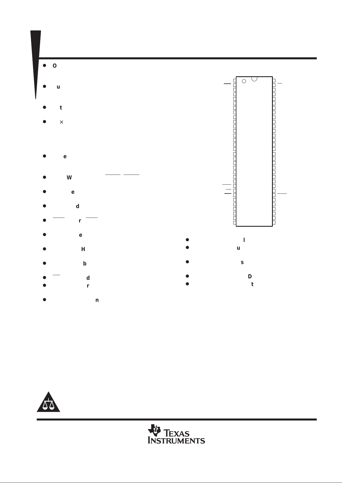
The SMJ55161 is offered in a 68-pin ceramic pin-grid-array package (GB suffix) and a 64-pin ceramic flatpack
(HKC suffix).
The SMJ55161 and other TI multiport-video RAMs are supported by a broad line of graphic processors and
control devices from TI. See Table 2 and Table 4 for additional information.
Page 5
SMJ55161
262144 BY 16-BIT
MULTIPORT VIDEO RAM
SGMS056D – MA Y 1995 – REVISED OCT OBER 1997
5
POST OFFICE BOX 1443 • HOUSTON, TEXAS 77251–1443
functional block diagram
Split-
Register
Status
SerialAddress
Counter
DRAM
Output
Buffer
DRAM
Input
Buffer
Input
Buffer
Row
Buffer
Column
Buffer
DQ0–
DQ15 A0–A8
DSF
1 of 4 Subblocks
(see next page)
1 of 4 Subblocks
(see next page)
1 of 4 Subblocks
(see next page)
1 of 4 Subblocks
(see next page)
QSF
SE
RAS
CASx
WE
TRG
Special-
Function
Logic
Refresh
Counter
Serial-
Output
Buffer
Timing
Generator
SQ0–
SQ15
SC
SE
16
16
9
Page 6
SMJ55161
262144 BY 16-BIT
MULTIPORT VIDEO RAM
SGMS056D – MA Y 1995 – REVISED OCT OBER 1997
6
POST OFFICE BOX 1443 • HOUSTON, TEXAS 77251–1443
functional block diagram (continued)
SE
1 of 4 Subblocks
Refresh
Counter
Row
Decoder
Split-
Register
Status
SerialAddress
Counter
Color
Register
Address
Mask
W/B
Latch
W/B
Unlatch
MUX
Write-
Per-Bit
Control
Serial-Data
Pointer
Serial-Data
Register
512 × 512
Memory
Array
Sense AMP
Column DEC
Special-
Function
Logic
Input
Buffer
DQi
DQi+1
DQi+2
DQi+3
RAS
CASx
TRG
WE
Column
Buffer
A0–A8
DSF
Row
Buffer
QSF
DRAM
Output
Buffer
DRAM
Input
Buffer
Timing
Generator
SQi
SQi + 1
SQi +2
SQi + 3
Serial-
Output
Buffer
SE
SC
9
Page 7
SMJ55161
262144 BY 16-BIT
MULTIPORT VIDEO RAM
SGMS056D – MA Y 1995 – REVISED OCT OBER 1997
7
POST OFFICE BOX 1443 • HOUSTON, TEXAS 77251–1443
functional operation description
Table 1 lists the DRAM and SAM functions, summarizing Table 3 and Table 4.
Table 1. DRAM and SAM Functions
RAS FALL
CASx
FALL
ADDRESS DQ0 –DQ15
†
FUNCTION
CASx‡TRG WE DSF DSF RAS CASx
§
RAS
CASL
CASU
WE
MNE
CODE
Reserved (do not use) L L L L X X X X X —
CBR refresh (no reset) and stop-point
set
¶
L X L H X
Stop
Point
#
X X X CBRS
CBR refresh (option reset)
||
L X H L X X X X X CBR
CBR refresh (no reset)
k
L X H H X X X X X CBRN
Full-register-transfer read H L H L X
Row
Address
Tap
Point
X X RT
Split-register-transfer read H L H H X
Row
Address
Tap
Point
X X SRT
DRAM write
(nonpersistent write-per-bit)
H H L L L
Row
Address
Column
Address
Write
Mask
Valid
Data
RWM
DRAM block write
(nonpersistent write-per-bit)
H H L L H
Row
Address
Block
Address
A2–A8
Write
Mask
Column
Mask
BWM
DRAM write
(persistent write-per-bit)
H H L L L
Row
Address
Column
Address
X
Valid
Data
RWM
DRAM block write
(persistent write-per-bit)
H H L L H
Row
Address
Block
Address
A2–A8
X
Column
Mask
BWM
DRAM write (nonmasked) H H H L L
Row
Address
Column
Address
X
Valid
Data
RW
DRAM block write (nonmasked) H H H L H
Row
Address
Block
Address
A2–A8
X
Column
Mask
BW
Load write-mask register
h
H H H H L
Refresh
Address
X X
Write
Mask
LMR
Load color register H H H H H
Refresh
Address
X X
Color
Data
LCR
Legend:
Col Mask = H: Write to address/column enabled
Write Mask = H: Write to I/O enabled
X = Don’t care
†
DQ0–DQ15 are latched on either the first falling edge of CASx
or the falling edge of WE, whichever occurs later.
‡
Logic L is selected when either or both CASL
and CASU are low.
§
The column address and block address are latched on the first falling edge of CASx
.
¶
CBRS cycle should be performed immediately after the powerup initialization cycle.
#
A0–A3, A8: don’t care; A4–A7: stop-point code
||
CBR refresh (option reset) mode ends persistent write-per-bit mode and stop-point mode.
k
CBR refresh (no reset) mode does not end persistent write-per-bit mode or stop-point mode.
h
Load-write-mask-register cycle sets the persistent write-per-bit mode. The persistent write-per-bit mode is reset only by the CBR (option reset)
cycle.
Page 8
SMJ55161
262144 BY 16-BIT
MULTIPORT VIDEO RAM
SGMS056D – MA Y 1995 – REVISED OCT OBER 1997
8
POST OFFICE BOX 1443 • HOUSTON, TEXAS 77251–1443
pin definitions
Table 2. Pin Description Versus Operational Mode
PIN DRAM TRANSFER SAM
A0 –A8 Row, column address Row address, tap point
CASL
CASU
Column-address strobe, DQ output enable Tap-address strobe
DQ DRAM data I/O, write mask
DSF
Block-write enable
Write-mask-register load enable
Color-register load enable
CBR (option reset)
Split-register-transfer enable
RAS Row-address strobe Row-address strobe
SE
SQ output enable,
QSF output enable
SC Serial clock
SQ Serial-data output
TRG DQ output enable Transfer enable
WE Write enable, write-per-bit enable
QSF Special-function output Serial-register status
NC/GND Either make no external connection or tie to system GND (VSS)
V
CC
†
5-V supply
V
SS
†
Ground
†
For proper device operation, all VCC pins must be connected to a 5-V supply, and all VSS pins must be tied to ground.
address (A0–A8)
Eighteen address bits are required to decode each one of the 262 144 storage cell locations. Nine row-address
bits are set up on pins A0–A8 and latched onto the chip on the falling edge of RAS
. Nine column-address bits
are set up on pins A0–A8 and latched onto the chip on the first falling edge of CASx
. All addresses must be
stable on or before the falling edge of RAS
and the first falling edge of CASx.
During the full-register-transfer read operation, the states of A0–A8 are latched on the falling edge of RAS
to
select one of the 512 rows where the transfer occurs. At the first falling edge of CASx
, the column-address bits
A0–A8 are latched. The most significant column-address bit (A8) selects which half of the row is transferred
to the SAM. The appropriate 8-bit column address (A0–A7) selects one of 256 tap points (starting positions)
for the serial-data output.
During the split-register-transfer read operation, address bit A7 is ignored at the falling edge of CASx
. An internal
counter selects which half of the register is used. If the high half of the SAM is currently in use, the low half of
the SAM is loaded with the low half of the DRAM half row and vice versa. Column address (A8) selects the DRAM
half row. The remaining seven address bits (A0–A6) are used to select one of 127 possible starting locations
within the SAM. Locations 127 and 255 are not valid tap points.
row-address strobe (RAS
)
RAS
is similar to a chip enable so that all DRAM cycles and transfer cycles are initiated by the falling edge of
RAS
. RAS is a control input that latches the states of the row address, WE, TRG, CASL, CASU, and DSF onto
the chip to invoke DRAM and transfer-read functions of the SMJ55161.
Page 9

SMJ55161
262144 BY 16-BIT
MULTIPORT VIDEO RAM
SGMS056D – MA Y 1995 – REVISED OCT OBER 1997
9
POST OFFICE BOX 1443 • HOUSTON, TEXAS 77251–1443
column-address strobe (CASL, CASU)
CASL
and CASU are control inputs that latch the states of the column address and DSF to control DRAM and
transfer functions of the SMJ55161. CASx
also acts as output enable for the DRAM output pins DQ0–DQ15.
In DRAM operation, CASL
enables data to be written to or read from the lower byte (DQ0–DQ7), and CASU
enables data to be written to or from the upper byte (DQ8–DQ15). In transfer operations, address bits A0–A8
are latched at the first falling edge of CASx
as the start position (tap) for the serial-data output (SQ0–SQ15).
output enable/transfer select (TRG
)
TRG
selects either DRAM or transfer operation as RAS falls. For DRAM operation, TRG must be held high as
RAS
falls. During DRAM operation, TRG functions as an output enable for the DRAM output pins DQ0–DQ15.
For transfer operation, TRG
must be brought low before RAS falls.
write-mask select, write enable (WE
)
In DRAM operation, WE
enables data to be written to the DRAM. WE is also used to select the DRAM
write-per-bit mode. Holding WE
low on the falling edge of RAS invokes the write-per-bit operation. The
SMJ55161 supports both the nonpersistent write-per-bit mode and the persistent write-per-bit mode.
special-function select (DSF)
The DSF input is latched on the falling edge of RAS
or the first falling edge of CASx, similar to an address. DSF
determines which of the following functions are invoked on a particular cycle:
D
CBR refresh with reset (CBR)
D
CBR refresh with no reset (CBRN)
D
CBR refresh with no reset and stop-point set (CBRS)
D
Block write
D
Loading write-mask register for the persistent write-per-bit mode (LMR)
D
Loading color register for the block-write mode
D
Split-register-transfer read
DRAM data I/O, write mask data (DQ0–DQ15)
DRAM data is written or read through the common I/O DQ pins. The 3-state DQ-output buffers provide direct
TTL compatibility (no pullup resistors) with a fanout of one Series 54 TTL load. Data out is the same polarity
as data in. During a normal access cycle, the outputs remain in the high-impedance state until TRG
is brought
low. Data appears at the outputs until TRG
returns high, CASx returns high following RAS returning high, or RAS
returns high following CASx returning high. The write mask is latched into the device through the random DQ
pins by the falling edge of RAS
and is used on all write-per-bit cycles. In a transfer operation, the DQ outputs
remain in the high-impedance state for the entire cycle.
serial-data outputs (SQ0 –SQ15)
Serial data is read from the SQ pins. The SQ output buffers provide direct TTL compatibility (no pullup resistors)
with a fanout of one Series 54 TTL load. The serial outputs are in the high-impedance (floating) state as long
as the serial-enable pin, SE
, is high. The serial outputs are enabled when SE is brought low.
serial clock (SC)
Serial data is accessed out of the data register during the rising edge of SC. The SMJ55161 is designed to work
with a wide range of clock duty cycles to simplify system design. There is no refresh requirement because the
data registers that comprise the SAM are static. There is also no minimum SC-clock operating frequency.
Page 10

SMJ55161
262144 BY 16-BIT
MULTIPORT VIDEO RAM
SGMS056D – MA Y 1995 – REVISED OCT OBER 1997
10
POST OFFICE BOX 1443 • HOUSTON, TEXAS 77251–1443
serial enable (SE)
During serial-access operations, SE
is used as an enable / disable for the SQ outputs. SE low enables the
serial-data output while SE
high disables the serial-data output. SE is also used as an enable/disable for output
pin QSF.
IMPORT ANT: While SE
is held high, the serial clock is not disabled. External SC pulses increment the internal
serial-address counter regardless of the state of SE
. This ungated serial-clock scheme minimizes access time
of serial output from SE
low because the serial-clock input buffer and the serial-address counter are not disabled
by SE
.
special-function output (QSF)
QSF is an output pin that indicates which half of the SAM is being accessed. When QSF is low, the serial-address
pointer is accessing the lower (least significant) 128 bits of the serial register (SAM). When QSF is high, the
pointer is accessing the higher (most significant) 128 bits of the SAM.
During full-register-transfer operations, QSF can change state upon completing the cycle. This state is
determined by the tap point loaded during the transfer cycle. QSF is enabled by SE
; therefore, if SE is high, the
QSF output is in the high-impedance state.
no connect /ground (NC/GND)
NC/GND must be tied to system ground or left floating for proper device operation.
Page 11
SMJ55161
262144 BY 16-BIT
MULTIPORT VIDEO RAM
SGMS056D – MA Y 1995 – REVISED OCT OBER 1997
11
POST OFFICE BOX 1443 • HOUSTON, TEXAS 77251–1443
random access operation
Table 3 lists the DRAM functions.
Table 3. DRAM Functions
RAS FALL
CASx
FALL
ADDRESS DQ0 –DQ15
†
FUNCTION
CASx‡TRG WE DSF DSF RAS CASx
§
RAS
CASL
CASU
WE
MNE
CODE
Reserved (do not use) L L L L X X X X X —
CBR refresh (no reset) and stop-point
set
¶
L X L H X
Stop
Point
#
X X X CBRS
CBR refresh (option reset)
||
L X H L X X X X X CBR
CBR refresh (no reset)
k
L X H H X X X X X CBRN
DRAM write
(nonpersistent write-per-bit)
H H L L L
Row
Address
Column
Address
Write
Mask
Valid
Data
RWM
DRAM block write
(nonpersistent write-per-bit)
H H L L H
Row
Address
Block
Address
A2–A8
Write
Mask
Column
Mask
BWM
DRAM write
(persistent write-per-bit)
H H L L L
Row
Address
Column
Address
X
Valid
Data
RWM
DRAM block write
(persistent write-per-bit)
H H L L H
Row
Address
Block
Address
A2–A8
X
Column
Mask
BWM
DRAM write (nonmasked) H H H L L
Row
Address
Column
Address
X
Valid
Data
RW
DRAM block write (nonmasked) H H H L H
Row
Address
Block
Address
A2–A8
X
Column
Mask
BW
Load write-mask register
h
H H H H L
Refresh
Address
X X
Write
Mask
LMR
Load color register H H H H H
Refresh
Address
X X
Color
Data
LCR
Legend:
Col Mask = H: Write to address/column enabled
Write Mask = H: Write to I/O enabled
X = Don’t care
†
DQ0–DQ15 are latched on either the first falling edge of CASx
or the falling edge of WE, whichever occurs later.
‡
Logic L is selected when either or both CASL
and CASU are low.
§
The column address and block address are latched on the first falling edge of CASx
.
¶
CBRS cycle should be performed immediately after the power-up initialization cycle.
#
A0–A3, A8: don’t care; A4–A7: stop-point code
||
CBR refresh (option reset) mode ends persistent write-per-bit mode and stop-point mode.
k
CBR refresh (no reset) mode does not end persistent write-per-bit mode or stop-point mode.
h
Load-write-mask-register cycle sets the persistent write-per-bit mode. The persistent write-per-bit mode is reset only by the CBR (option reset)
cycle.
Page 12

SMJ55161
262144 BY 16-BIT
MULTIPORT VIDEO RAM
SGMS056D – MA Y 1995 – REVISED OCT OBER 1997
12
POST OFFICE BOX 1443 • HOUSTON, TEXAS 77251–1443
enhanced page mode
Enhanced page-mode operation allows faster memory access by keeping the same row address while selecting
random column addresses. This mode eliminates the time required for row-address setup, row-address hold,
and address multiplex. The maximum RAS
low time and CAS page cycle time used determine the number of
columns that can be accessed.
Unlike conventional page-mode operations, the enhanced page mode allows the SMJ55161 to operate at a
higher data bandwidth. Data retrieval begins as soon as the column address is valid rather than when CASx
transitions low. A valid column address can be presented immediately after the row-address hold time has been
satisfied, usually well in advance of the falling edge of CASx
. In this case, data is obtained after t
a(C)
MAX
(access time from CASx
low) if t
a(CA)
MAX (access time from column address) has been satisfied.
refresh
CAS-before-RAS (CBR) refresh
CBR refreshes are accomplished by bringing either or both CASL and CASU low earlier than RAS. The external
row address is ignored, and the refresh row address is generated internally . Three types of CBR refresh cycles
are available. The CBR refresh (option reset) ends the persistent write-per-bit mode and the stop-point mode.
The CBRN and CBRS refreshes (no reset) do not end the persistent write-per-bit mode or the stop-point mode.
The 512 rows of the DRAM do not necessarily need to be refreshed consecutively as long as the entire refresh
is completed within the required time period, t
rf(MA)
. The output buffers remain in the high-impedance state
during the CBR refresh cycles regardless of the state of TRG
.
hidden refresh
A hidden refresh is accomplished by holding both CASL and CASU low in the DRAM read cycle and cycling
RAS
. The output data of the DRAM read cycle remains valid while the refresh is carried out. Like the CBR
refresh, the refreshed row addresses are generated internally during the hidden refresh.
RAS-only refresh
A RAS-only refresh is accomplished by cycling RAS at every row address. Unless CASx and TRG are low, the
output buffers remain in the high-impedance state to conserve power. Externally-generated addresses must
be supplied during RAS
-only refresh. Strobing each of the 512 row addresses with RAS causes all bits in each
row to be refreshed.
Page 13
SMJ55161
262144 BY 16-BIT
MULTIPORT VIDEO RAM
SGMS056D – MA Y 1995 – REVISED OCT OBER 1997
13
POST OFFICE BOX 1443 • HOUSTON, TEXAS 77251–1443
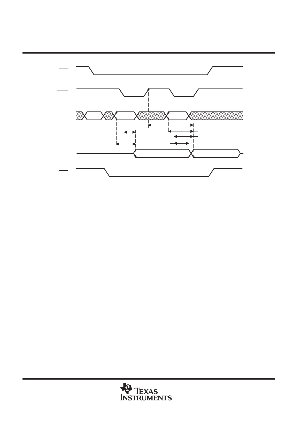
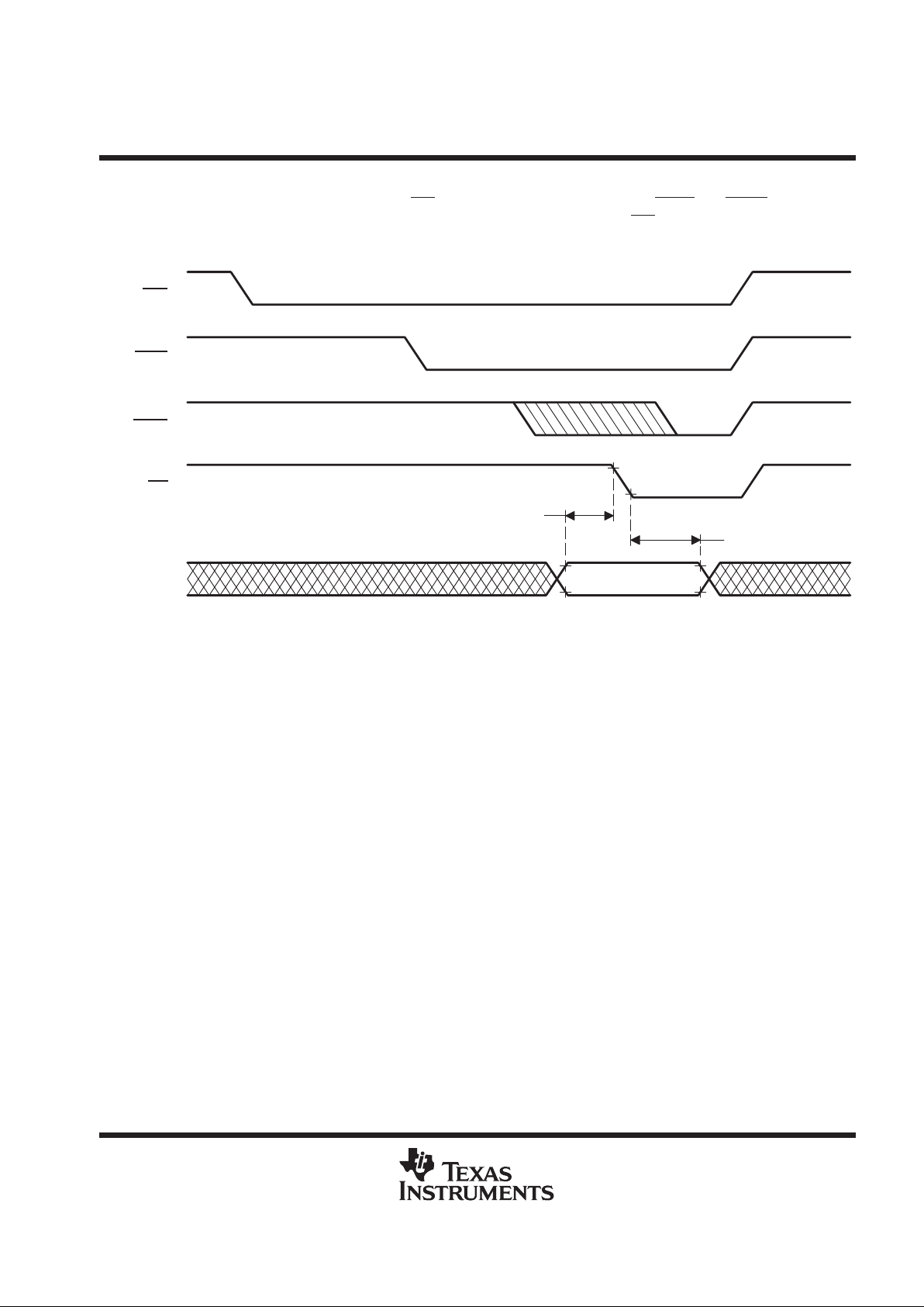
extended data output
The SMJ55161 features EDO during DRAM accesses. While RAS
and TRG are low, the DRAM output remains
valid. The output remains valid even when CASx
returns high until WE is low, TRG is high, or both CASx and
RAS
are high (see Figure 1 and Figure 2). The EDO mode functions during all read cycles including DRAM read,
page-mode read, and read-modify-write cycles (see Figure 3).
RAS
CASx
DQ0–DQ15
TRG
Valid Output
t
dis(RH)
t
dis(G)
Figure 1. DRAM Read Cycle With RAS-Controlled Output
RAS
CASx
DQ0–DQ15
TRG
Valid Output
t
dis(CH)
t
dis(G)
Figure 2. DRAM Read Cycle With CASx-Controlled Output
Page 14
SMJ55161
262144 BY 16-BIT
MULTIPORT VIDEO RAM
SGMS056D – MA Y 1995 – REVISED OCT OBER 1997
14
POST OFFICE BOX 1443 • HOUSTON, TEXAS 77251–1443
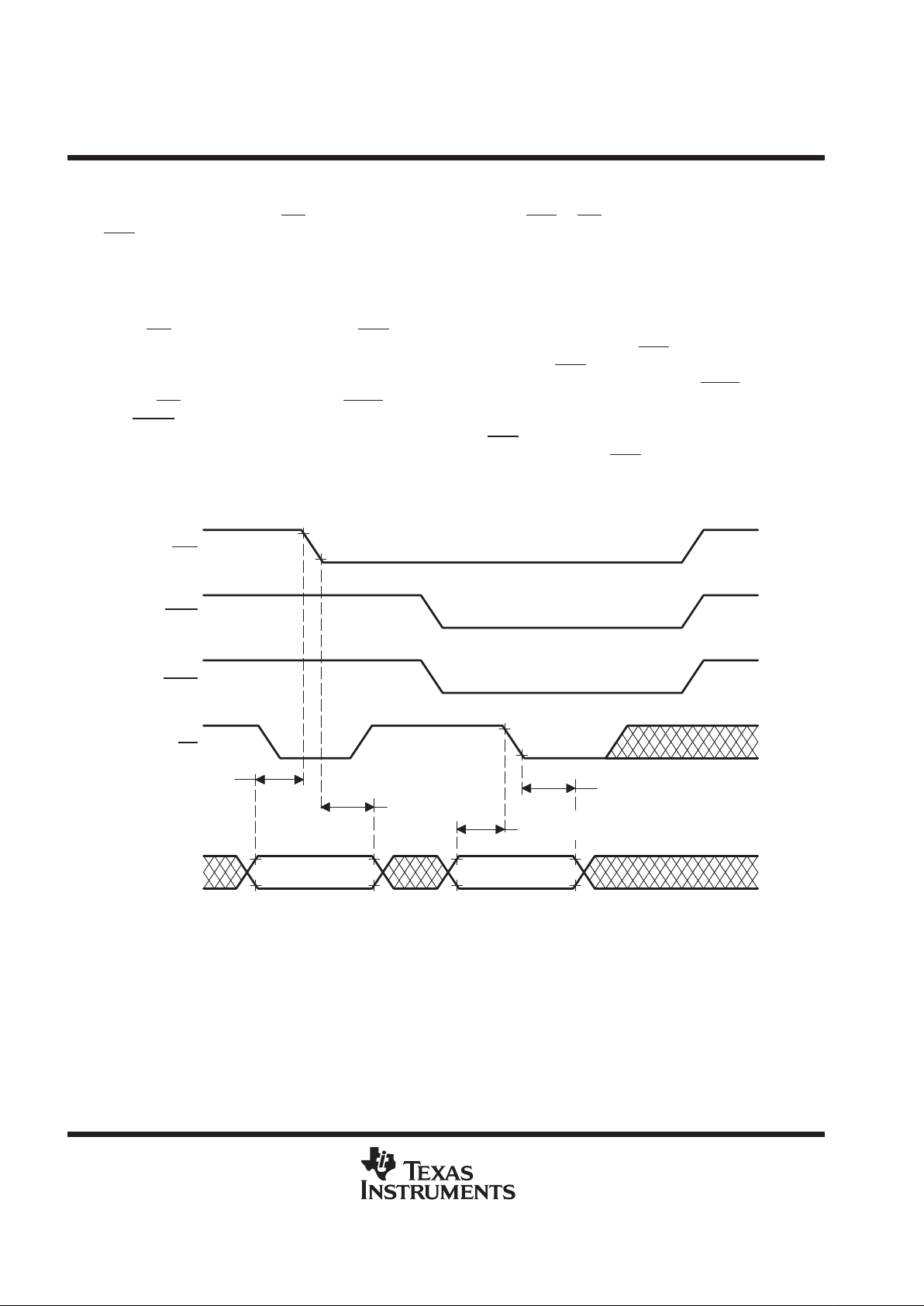
extended-data output (continued)
RAS
A0–A8
DQ0–DQ15
Valid Output
t
a(CA)
Row
CASx
TRG
Valid Output
t
a(C)
t
h(CLQ)
t
a(C)
t
a(CP)
Column Column
t
a(CA)
Figure 3. DRAM Page-Read Cycle With Extended Output
Page 15
SMJ55161
262144 BY 16-BIT
MULTIPORT VIDEO RAM
SGMS056D – MA Y 1995 – REVISED OCT OBER 1997
15
POST OFFICE BOX 1443 • HOUSTON, TEXAS 77251–1443
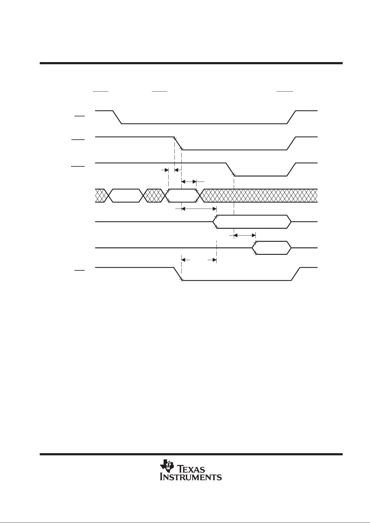
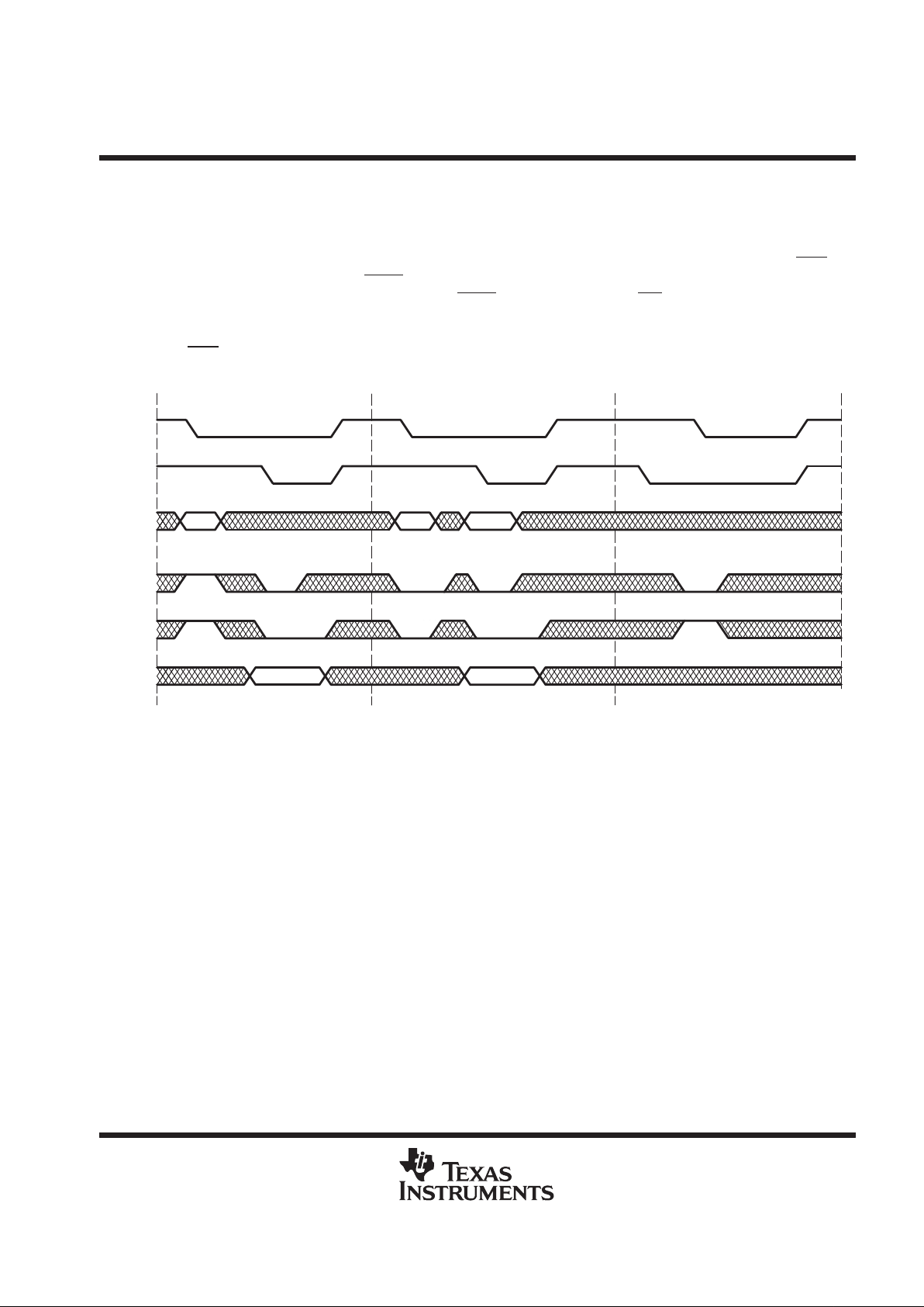
byte operation
Byte operation can be applied in DRAM-read cycles, write cycles, block-write cycles, load-write-mask-register
cycles, and load-color-register cycles. In byte operation, the column address (A0 –A8) is latched at the first
falling edge of CASx
. In read cycles, CASL enables the lower byte (DQ0–DQ7) and CASU enables the upper
byte (DQ8–DQ15) (see Figure 4).
Row
t
h(CLCA)
RAS
t
su(CA)
Column
Lower Byte Output
Upper Byte
Output
t
a(C)
CASL
CASU
A0–A8
DQ0–DQ7
DQ8–DQ15
TRG
t
a(G)
t
a(C)
Figure 4. Example of a Byte-Read Cycle
Page 16
SMJ55161
262144 BY 16-BIT
MULTIPORT VIDEO RAM
SGMS056D – MA Y 1995 – REVISED OCT OBER 1997
16
POST OFFICE BOX 1443 • HOUSTON, TEXAS 77251–1443
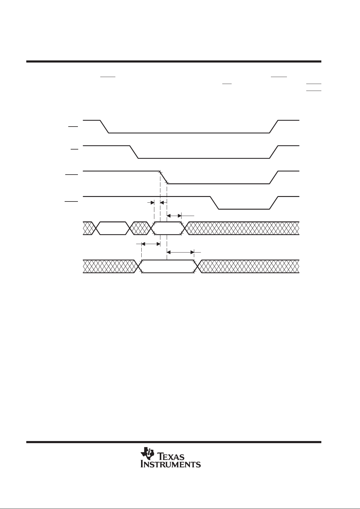
byte operation (continued)
In byte-write operation, CASL
enables data to be written to the lower byte (DQ0–DQ7), and CASU enables data
to be written to the upper byte (DQ8 –DQ15). In an early write cycle, WE
is brought low prior to both CASx
signals, and data setup and hold times for DQ0 – DQ15 are referenced to the first falling edge of CASx
(see Figure 5).
RAS
WE
CASU
A0–A8
DQ0–DQ15
Valid Input
t
h(CLD)
t
su(DCL)
CASL
t
h(CLCA)
t
su(CA)
Row Column
Figure 5. Example of an Early-Write Cycle
Page 17
SMJ55161
262144 BY 16-BIT
MULTIPORT VIDEO RAM
SGMS056D – MA Y 1995 – REVISED OCT OBER 1997
17
POST OFFICE BOX 1443 • HOUSTON, TEXAS 77251–1443
byte operation (continued)
For late-write or read-modify-write cycles, WE
is brought low after either or both CASL and CASU fall. The data
is strobed in with data setup and hold times for DQ0–DQ15 referenced to WE
(see Figure 6).
RAS
CASL
CASU
WE
DQ0–DQ15
Valid Input
t
h(WLD)
t
su(DWL)
Figure 6. Example of a Late-Write Cycle
Page 18
SMJ55161
262144 BY 16-BIT
MULTIPORT VIDEO RAM
SGMS056D – MA Y 1995 – REVISED OCT OBER 1997
18
POST OFFICE BOX 1443 • HOUSTON, TEXAS 77251–1443
write-per-bit
The write-per-bit feature allows masking any combination of the 16 DQs on any write cycle. The write-per-bit
operation is invoked when WE is held low on the falling edge of RAS. If WE is held high on the falling edge of
RAS
, the write operation is performed without any masking. The SMJ55161 offers two write-per-bit modes:
nonpersistent write-per-bit and persistent write-per-bit.
nonpersistent write-per-bit
When WE is low on the falling edge of RAS, the write mask is reloaded. A 16-bit binary code (the write-per-bit
mask) is input to the device through the DQ pins and latched on the falling edge of RAS
. The write-per-bit mask
selects which of the 16 I/Os are to be written and which are not. After RAS
has latched the on-chip write-per-bit
mask, input data is driven onto the DQ pins and is latched on either the first falling edge of CASx
or the falling
edge of WE
, whichever occurs later. CASL enables the lower byte (DQ0–DQ7) to be written through the mask
and CASU
enables the upper byte (DQ8–DQ15) to be written through the mask. If a data low (write mask = 0)
is strobed into a particular I /O pin on the falling edge of RAS
, data is not written to that I /O. If a data high
(write mask = 1) is strobed into a particular I / O pin on the falling edge of RAS
, data is written to that I / O
(see Figure 7).
RAS
CASL
CASU
WE
DQ0–DQ15 Valid Input
t
h(WLD)
t
su(DQR)
t
su(DWL)
t
h(RDQ)
Write Mask
Figure 7. Example of a Nonpersistent Write-Per-Bit (Late-Write) Operation
Page 19
SMJ55161
262144 BY 16-BIT
MULTIPORT VIDEO RAM
SGMS056D – MA Y 1995 – REVISED OCT OBER 1997
19
POST OFFICE BOX 1443 • HOUSTON, TEXAS 77251–1443
persistent write-per-bit
The persistent write-per-bit mode is initiated by performing a load-write-mask-register (LMR) cycle. In the
persistent write-per-bit mode, the write-per-bit mask is overwritten but remains valid over an arbitrary number
of write cycles until another LMR cycle is performed or power is removed.
The LMR cycle is performed using DRAM write-cycle timing with DSF held high on the falling edge of RAS
and
held low on the first falling edge of CASx
. A binary code is input to the write-mask register via the random I/O
pins and latched on either the first falling edge of CASx
or the falling edge of WE, whichever occurs later. Byte
write control can be applied to the write mask during the LMR cycle. The persistent write-per-bit mode can then
be used in exactly the same way as the nonpersistent write-per-bit mode except that the input data on the falling
edge of RAS
is ignored. When the device is set to the persistent write-per-bit mode, it remains in this mode and
is reset only by a CBR refresh (option-reset) cycle (see Figure 8).
RAS
CASx
A0–A8
DSF
Load-Write-Mask Register Persistent Write-Per-Bit
DQ0–
DQ15
Write-Mask
Data
Valid
Input
CBR Refresh (option reset)
WE
Refresh
Address
Row Column
Mask Data = 1: Write to I/O enabled
= 0: Write to I/O disabled
Figure 8. Example of a Persistent Write-Per-Bit Operation
Page 20
SMJ55161
262144 BY 16-BIT
MULTIPORT VIDEO RAM
SGMS056D – MA Y 1995 – REVISED OCT OBER 1997
20
POST OFFICE BOX 1443 • HOUSTON, TEXAS 77251–1443
block write
The block-write feature allows up to 64 bits of data to be written simultaneously to one row of the memory array .
This function is implemented as four columns by four DQs and repeated in four quadrants. In this manner, each
of the four 1M-bit quadrants can have up to four consecutive columns written at a time with up to four DQs per
column (see Figure 9).
DQ4
DQ14
DQ0
Four Consecutive Columns of 0–511
DQ1
DQ2
DQ3
DQ5
DQ6
DQ7
DQ8
DQ9
DQ10
DQ11
DQ12
DQ13
DQ15
4th Quadrant
3rd Quadrant
2nd Quadrant
1st Quadrant
One Row of 0–511
Figure 9. Block-Write Operation
Each 1M-bit quadrant has a 4-bit column mask to mask off and prevent any or all of the four columns from being
written with data. Nonpersistent write-per-bit or persistent write-per-bit functions can be applied to the
block-write operation to provide write-masking options. The DQ data is provided by 4 bits from the on-chip color
register. Bits 0–3 from the 16-bit write-mask register, bits 0–3 from the 16-bit column-mask register, and bits
0–3 from the 16-bit color-data register configure the block write for the first quadrant, while bits 4 –7, 8–11,
and 12–15 of the corresponding registers control the other quadrants in a similar fashion (see Figure 10).
Page 21

SMJ55161
262144 BY 16-BIT
MULTIPORT VIDEO RAM
SGMS056D – MA Y 1995 – REVISED OCT OBER 1997
21
POST OFFICE BOX 1443 • HOUSTON, TEXAS 77251–1443
block write (continued)
3
1
DQ0
DQ1
DQ2
DQ3
DQ4
DQ5
DQ6
DQ7
DQ8
DQ9
DQ10
DQ11
DQ12
DQ13
DQ14
DQ15
One Row of 0–511
0
1
2
3
0
2
7
5
4
5
6
7
4
6
11
9
8
9
10
11
8
10
15
13
12
13
14
15
12
14
Color Register
0 1 2 3 4 5 6 7 8 9 10 11 12 13 14 15
Column MaskWrite Mask
Figure 10. Block Write With Masks
Page 22

SMJ55161
262144 BY 16-BIT
MULTIPORT VIDEO RAM
SGMS056D – MA Y 1995 – REVISED OCT OBER 1997
22
POST OFFICE BOX 1443 • HOUSTON, TEXAS 77251–1443
block write (continued)
A set of four columns makes a block, resulting in 128 blocks along one row. Block 0 comprises columns 0–3,
block 1 comprises columns 4–7, block 2 comprises columns 8 –1 1, etc., as shown in Figure 11.
01234567 511. . . . . . . . . . . . . . . . . . . . . . . . . . .
Columns
Block 0 Block 1 Block 127. . . . . . . . . . . . . . . . . . . . . .
One Row of 0–511
Figure 11. Block Columns Organization
During block-write cycles, only the seven most significant column addresses (A2–A8) are latched on the first
falling edge of CASx
to decode one of the 128 blocks. Address bits A0–A1 are ignored. Each 1M-bit quadrant
has the same block selected.
A block-write cycle is entered in a manner similar to a DRAM write cycle except DSF is held high on the first
falling edge of CASx
. As in a DRAM write operation, CASL and CASU enable the corresponding lower and upper
DRAM DQ bytes to be written. The column-mask data is input via the DQs and is latched on either the first falling
edge of CASx
or the falling edge of WE, whichever occurs later. The 16-bit color-data register must be loaded
prior to performing a block write as described below. Refer to the write-per-bit section for details on use of the
write-mask capability, allowing additional performance options.
Example of block write:
Block-write column address = 110000000 (A0–A8 from left to right)
bit 0 bit 15
Color-data register = 1011 1011 1100 0111
Write-mask register = 1110 1111 1111 1011
Column-mask register = 1111 0000 0111 1010
1st 2nd 3rd 4th
Quad Quad Quad Quad
Column-address bits A0 and A1 are ignored. Block 0 (columns 0–3) is selected for each 1M-bit quadrant. The
first quadrant has DQ0–DQ2 written with bits 0–2 from the color-data register (101) to all four columns of block
0. DQ3 is not written and retains its previous data due to write-mask-register-bit 3 being 0.
The second quadrant (DQ4–DQ7) has all four columns masked off due to column-mask bits 4–7 being 0 so
that no data is written.
The third quadrant (DQ8–DQ1 1 ) has its four DQs written with bits 8–11 from the color-data register (1 100) to
columns 1 – 3 of its block 0. Column 0 is not written and retains its previous data on all four DQs due to
column-mask-register-bit 8 being 0.
Page 23

SMJ55161
262144 BY 16-BIT
MULTIPORT VIDEO RAM
SGMS056D – MA Y 1995 – REVISED OCT OBER 1997
23
POST OFFICE BOX 1443 • HOUSTON, TEXAS 77251–1443
block write (continued)
The fourth quadrant (DQ12 –DQ15 ) has DQ12, DQ14, and DQ15 written with bits 12, 14, and 15 from the
color-data register to column 0 and column 2 of its block 0. DQ13 retains its previous data on all columns due
to the write mask. Columns 1 and 3 retain their previous data on all DQs due to the column mask. If the previous
data for the quadrant is all 0s, the fourth quadrant contains the data pattern shown in Figure 12 after the
block-write operation shown in the previous example.
DQ12
Columns 0 1 2 3
4th Quadrant
0000
DQ13 0 0 0 0
DQ14 1 0 1 0
DQ15 1 0 1 0
Figure 12. Example of Fourth Quadrant After a Block-Write Operation
load color register
The load-color-register cycle is performed using normal DRAM write-cycle timing except that DSF is held high
on the falling edges of RAS
, CASL, and CASU. The color register is loaded from pins DQ0–DQ15, which are
latched on either the first falling edge of CASx
or the falling edge of WE, whichever occurs later. If only one CASx
is low, only the corresponding byte of the color register is loaded. When the color register is loaded, it retains
data until power is lost or until another load-color-register cycle is performed (see Figure 13 and Figure 14).
RAS
CASx
A0–A8
WE
TRG
DSF
DQ0–DQ15
12323
4656
Load-Color-Register Cycle
Block-Write Cycle
(no write mask)
Block-Write Cycle
(load and use write mask)
Legend:
1. Refresh address
2. Row address
3. Block address (A2–A8) is latched on the first falling edge of CASx
.
4. Color-register data
5. Write-mask data: DQ0–DQ15 are latched on the falling edge of RAS
.
6. Column-mask data: DQi–DQi+3 (i = 0, 4, 8, 12) are latched on either the first falling edge of CASx
or the falling edge of WE, whichever
occurs later.
= don’t care
Figure 13. Example of Block Writes
Page 24

SMJ55161
262144 BY 16-BIT
MULTIPORT VIDEO RAM
SGMS056D – MA Y 1995 – REVISED OCT OBER 1997
24
POST OFFICE BOX 1443 • HOUSTON, TEXAS 77251–1443
load color register (continued)
RAS
CASx
A0–A8
WE
TRG
DSF
DQ0–DQ15
1 23
5
6
Load-Write-Mask-Register Cycle
Load-Color-Register Cycle
Persistent Block-Write Cycle
(use loaded write mask)
1
4
Legend:
1. Refresh address
2. Row address
3. Block address (A2–A8) is latched on the first falling edge of CASx
.
4. Color-register data
5. Write-mask data: DQ0–DQ15 are latched on the falling edge of RAS
.
6. Column-mask data: DQi–DQi+3 (i = 0, 4, 8, 12) are latched on either the first falling edge of CASx
or the falling edge of WE, whichever
occurs later.
= don’t care
Figure 14. Example of a Persistent Block Write
DRAM-to-SAM transfer operation
During the DRAM-to-SAM transfer operation, one half of a row (256 columns) in the DRAM array is selected
to be transferred to the 256-bit serial-data register. The transfer operation is invoked by TRG
being brought low
and WE
being held high on the falling edge of RAS. The state of DSF, which is latched on the falling edge of
RAS
, determines whether the full-register-transfer read operation or the split-register-transfer read operation
is performed (see Table 4).
Table 4. SAM Function Table
RAS FALL
CASx
FALL
ADDRESS DQ0–DQ15
MNE
FUNCTION
CASx†TRG WE DSF DSF RAS CASx RAS
CASx
WE
CODE
Full-register-transfer read H L H L X
Row
Addr
Tap
Point
X X RT
Split-register-transfer read H L H H X
Row
Addr
Tap
Point
X X SRT
†
Logic L is selected when either CASL or CASU are low.
X = don’t care
Page 25

SMJ55161
262144 BY 16-BIT
MULTIPORT VIDEO RAM
SGMS056D – MA Y 1995 – REVISED OCT OBER 1997
25
POST OFFICE BOX 1443 • HOUSTON, TEXAS 77251–1443
full-register-transfer read
A full-register-transfer read operation loads data from a selected half of a row in the DRAM into the SAM. TRG
is brought low and latched at the falling edge of RAS. Nine row-address bits (A0–A8) are also latched at the
falling edge of RAS
to select one of the 512 rows available for the transfer. The nine column-address bits
(A0 – A8) are latched at the first falling edge of CASx
, where address bit A8 selects which half of the row is
transferred. Address bits A0–A7 select one of the SAM’s 256 available tap points from which the serial data
is read out (see Figure 15).
512 × 512
Memory Array
256-Bit
Data Register
0 255 256 511
0 255
A8 = 0 A8 = 1
Figure 15. Full-Register-Transfer Read
A full-register-transfer read can be performed in three ways: early load, real-time load (or midline load), or late
load. Each of these offers the flexibility of controlling the TRG
trailing edge in the full-register-transfer read cycle
(see Figure 16).
Early Load Real-Time Load Late Load
RAS
CASx
A0–A8
TRG
WE
Row Tap
Point
Row Tap
Point
Row Tap
Point
SC
Tap
Bit
Tap
Bit
Tap
Bit
Old
Data
Old
Data
Old
Data
Old
Data
Old
Data
Figure 16. Example of Full-Register-Transfer Read Operations
Page 26

SMJ55161
262144 BY 16-BIT
MULTIPORT VIDEO RAM
SGMS056D – MA Y 1995 – REVISED OCT OBER 1997
26
POST OFFICE BOX 1443 • HOUSTON, TEXAS 77251–1443
split-register-transfer read
In the split-register-transfer-read operation, the serial-data register is split into halves. The low half contains bits
0–127, and the high half contains bits 128–255. While one half is being read out of the SAM port, the other
half can be loaded from the memory array.
512 × 512
Memory Array
256-Bit
Data Register
0 255 256 511
0 255
A8 = 0 A8 = 1
Figure 17. Split-Register-Transfer Read
To invoke a split-register-transfer-read cycle, DSF is brought high, TRG is brought low, and both are latched
at the falling edge of RAS
. Nine row-address bits (A0–A8) are also latched at the falling edge of RAS to select
one of the 512 rows available for the transfer. Eight of the nine column-address bits (A0–A6 and A8) are latched
at the first falling edge of CASx
. Column-address bit A8 selects which half of the row is to be transferred.
Column-address bits A0–A6 selects one of the 127 tap points in the specified half of the SAM. Column-address
bit A7 is ignored, and the split-register transfer is controlled internally to select the inactive register half.
Full XFER
RAS
Split XFER Split XFER Split XFER
AB
0511
A8 = 0
AB
0 255
SQ
ABC
0 A7 = 0†511
A8 = 1
CB
0 255
ABCD
0 A7 = 1†511
A8 = 1
CD
0 255
SQ
ABCD
E
0 A7 = 0
†
511
A8 = 0
ED
0 255
SQ
SQ
DRAM
SAM
†
A7 shown as internally controlled.
Figure 18. Example of a Split-Register-Transfer Read Operation
A full-register-transfer-read cycle must precede the first split-register-transfer-read cycle to ensure proper
operation. After the full-register-transfer-read cycle, the first split-register-transfer-read cycle can follow
immediately without any minimum SC-clock requirement.
Page 27

SMJ55161
262144 BY 16-BIT
MULTIPORT VIDEO RAM
SGMS056D – MA Y 1995 – REVISED OCT OBER 1997
27
POST OFFICE BOX 1443 • HOUSTON, TEXAS 77251–1443
split-register-transfer read (continued)
QSF indicates which half of the register is being accessed during serial-access operation. When QSF is low,
the serial-address pointer is accessing the lower (least significant) 128 bits of the SAM. When QSF is high, the
pointer is accessing the higher (most significant) 128 bits of the SAM. QSF changes state upon completing a
full-register-transfer-read cycle. The tap point loaded during the current transfer cycle determines the state of
QSF. QSF also changes state when a boundary between two register halves is reached.
RAS
CASx
DSF
TRG
QSF
SC
Tap
Point N
t
d(GHQSF)
Full-Register-Transfer Read
With Tap Point N
Split-Register-
Transfer Read
t
d(CLQSF)
Figure 19. Example of a Split-Register-Transfer Read After a Full-Register-Transfer Read
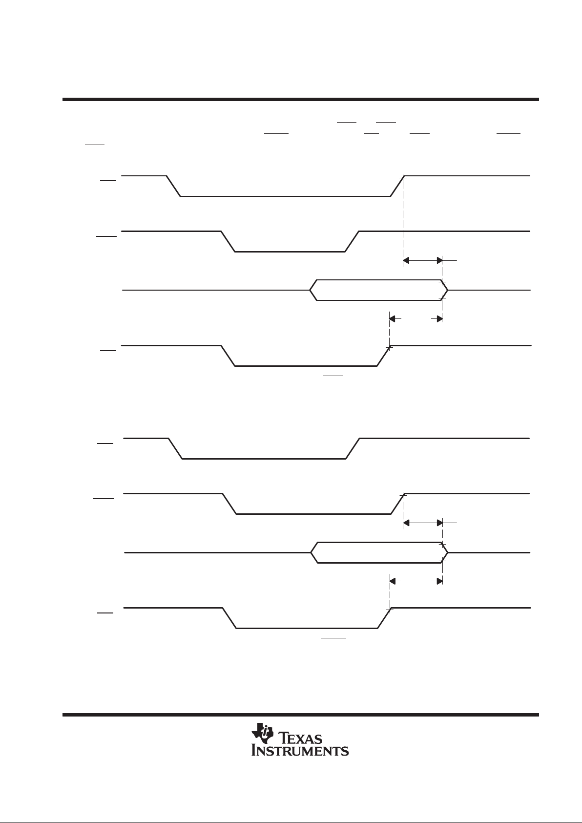
127
or 255
t
d(SCQSF)
RAS
CASx
DSF
TRG
QSF
SC
Tap
Point N
Split-Register-
Transfer Read
With Tap Point N
Split-RegisterTransfer Read
t
d(MSRL)
t
d(RHMS)
Figure 20. Example of Successive Split-Register-Transfer-Read Operations
Page 28

SMJ55161
262144 BY 16-BIT
MULTIPORT VIDEO RAM
SGMS056D – MA Y 1995 – REVISED OCT OBER 1997
28
POST OFFICE BOX 1443 • HOUSTON, TEXAS 77251–1443
serial-read operation
The serial-read operation can be performed through the SAM port simultaneously and asynchronously with
DRAM operations except during transfer operations. Serial data can be read from the SAM by clocking SC
starting at the tap point loaded by the preceding transfer cycle, proceeding sequentially to the most significant
bit (bit 255), and then wrapping around to the least significant bit (bit 0), as shown in Figure 21.
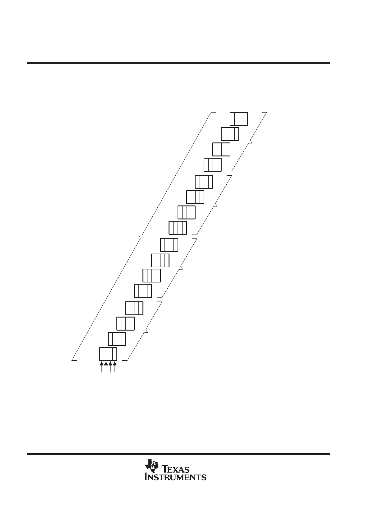
255254Tap210
Figure 21. Serial-Pointer Direction for Serial Read
For split-register-transfer-read operation, serial data can be read out from the active half of the SAM by clocking
SC starting at the tap point loaded by the preceding split-register-transfer cycle. The serial pointer then proceeds
sequentially to the most significant bit of the half, bit 127 or bit 255. If there is a split-register-transfer read to
the inactive half during this period, the serial pointer points next to the tap point location loaded by that
split-register transfer (see Figure 22).
127126Tap0 255254Tap128
Figure 22. Serial Pointer for Split-Register Read – Case I
If there is no split-register-transfer read to the inactive half during this period, the serial pointer points next to
bit 128 or bit 0, respectively (see Figure 23).
127126Tap0 255254Tap128
Figure 23. Serial Pointer for Split-Register Read – Case II
split-register programmable stop point
The SMJ55161 offers a programmable stop-point mode for split-register-transfer read operations. This mode
can be used to improve two-dimensional drawing performance in a nonscanline data format.
For a split-register-transfer-read operation, the stop point is defined as a register location at which the serial
output stops coming from one half of the SAM and switches to the opposite half of the SAM. While in stop-point
mode, the SAM is divided into partitions whose length is programmed via row addresses A4–A7 in a CBR set
(CBRS) cycle. The last serial-address location of each partition is the stop point (see Figure 24).
255128
0
127
Partition
Length
Stop
Points
Figure 24. Example of the SAM With Partitions
Page 29

SMJ55161
262144 BY 16-BIT
MULTIPORT VIDEO RAM
SGMS056D – MA Y 1995 – REVISED OCT OBER 1997
29
POST OFFICE BOX 1443 • HOUSTON, TEXAS 77251–1443
split-register programmable stop point (continued)
Stop-point mode is not active until the CBRS cycle is initiated. The CBRS operation is enabled by holding CASx
and WE low and DSF high on the falling edge of RAS. The falling edge of RAS also latches row addresses
A4 – A7 which are used to define the SAM’s partition length. The other row-address inputs are don’t cares.
Stop-point mode should be initiated after the initialization cycles are performed (see Table 5).
Table 5. Programming Code for Stop-Point Mode
MAXIMUM
ADDRESS AT RAS IN CBRS CYCLE
NUMBER OF
PARTITION
LENGTH
A8 A7 A6 A5 A4 A0– A3
PARTITIONS
STOP-POINT LOCATIONS
16 X L L L L X 16
15, 31, 47, 63, 79, 95, 111, 127, 143, 159, 175,
191, 207, 223, 239, 255
32 X L L L H X 8 31, 63, 95, 127, 159, 191, 223, 255
64 X L L H H X 4 63, 127, 191, 255
128
(default)
X L H H H X 2 127, 255
In stop-point mode, the tap point loaded during the split-register-transfer read cycle determines the SAM
partition in which the serial output begins and at which stop point the serial output stops coming from one half
of the SAM and switches to the opposite half of the SAM (see Figure 25).
255128
0
127
RAS
Read XFER
Split
Read XFER
Split
Tap = H1
SC
191
Tap = L1 Tap = H2
L1
63 H2
Read XFER
Split
Tap = L2
255 L2
63 191
SAM High HalfSAM Low Half
H1
L1 H1
Read XFER
Full
L2 H2
Figure 25. Example of Split-Register Operation With Programmable Stop Points
Page 30

SMJ55161
262144 BY 16-BIT
MULTIPORT VIDEO RAM
SGMS056D – MA Y 1995 – REVISED OCT OBER 1997
30
POST OFFICE BOX 1443 • HOUSTON, TEXAS 77251–1443
256-/512-bit compatibility of split-register programmable stop point
The stop-point mode is designed to be compatible with both 256-bit SAM and 512-bit SAM devices. After the
CBRS cycle is initiated, the stop-point mode becomes active. In stop-point mode only , column-address bits AY7
and AY8 are internally swapped to assure compatibility (see Figure 26). This address-bit swap applies to the
column address and is effective for all DRAM and transfer cycles. For example, during the split-register-transfer
cycle with stop point, column-address bit AY8 is a don’t care and AY7 decodes the DRAM half-row for the
split-register transfer. During stop-point mode, a CBR (option reset) cycle is not recommended because this
ends the stop-point mode and restores address bits A Y7 and AY8 to their normal functions. Consistent use of
CBR cycles ensures that the SMJ55161 remains in normal mode.
512 × 512
Memory Array
256-Bit
Data Register
A Y7 = 0 AY7 = 1 AY7 = 0 AY7 = 1
0 255
A Y8 = 0 AY8 = 1
512 × 512
Memory Array
256-Bit
Data Register
A Y7 = 0 AY7 = 1 AY7 = 0 AY7 = 1
0 255
A Y8 = 0 AY8 = 1
NONSTOP-POINT MODE STOP-POINT MODE
Figure 26. DRAM-to-SAM Mapping, Nonstop-Point Versus Stop Point
IMPORTANT: For proper device operation, a stop-point-mode (CBRS) cycle should be initiated immediately
after the power-up initialization cycles are performed.
power up
T o achieve proper device operation, an initial pause of 200 µs is required after power up followed by a minimum
of eight RAS
cycles or eight CBR cycles to initialize the DRAM port. A full-register-transfer-read cycle and two
SC cycles are required to initialize the SAM port.
After initialization, the internal state of the SMJ55161 is as shown in Table 6.
Table 6. Internal State of SMJ55161
STATE AFTER INITIALIZATION
QSF
Write mode
Write-mask register
Color register
Serial-register tap point
SAM port
Defined by the transfer cycle during initialization
Nonpersistent mode
Undefined
Undefined
Defined by the transfer cycle during initialization
Output mode
Page 31

SMJ55161
262144 BY 16-BIT
MULTIPORT VIDEO RAM
SGMS056D – MA Y 1995 – REVISED OCT OBER 1997
31
POST OFFICE BOX 1443 • HOUSTON, TEXAS 77251–1443
absolute maximum ratings over operating free-air temperature range (unless otherwise noted)
†
Supply voltage range, V
CC
(see Note 1) –1 V to 7 V. . . . . . . . . . . . . . . . . . . . . . . . . . . . . . . . . . . . . . . . . . . . . . . .
Voltage range on any pin –1 V to 7 V. . . . . . . . . . . . . . . . . . . . . . . . . . . . . . . . . . . . . . . . . . . . . . . . . . . . . . . . . . . . .
Short-circuit output current 50 mA. . . . . . . . . . . . . . . . . . . . . . . . . . . . . . . . . . . . . . . . . . . . . . . . . . . . . . . . . . . . . . . .
Power dissipation 1.1 W. . . . . . . . . . . . . . . . . . . . . . . . . . . . . . . . . . . . . . . . . . . . . . . . . . . . . . . . . . . . . . . . . . . . . . . . .
Operating free-air temperature range, T
A
– 55°C to 125°C. . . . . . . . . . . . . . . . . . . . . . . . . . . . . . . . . . . . . . . . . .
Storage temperature range, T
stg
–65°C to 150°C. . . . . . . . . . . . . . . . . . . . . . . . . . . . . . . . . . . . . . . . . . . . . . . . . . .
†
Stresses beyond those listed under “absolute maximum ratings” may cause permanent damage to the device. These are stress ratings only, and
functional operation of the device at these or any other conditions beyond those indicated under “recommended operating conditions” is not
implied. Exposure to absolute-maximum-rated conditions for extended periods may affect device reliability.
NOTE 1: All voltage values are with respect to VSS.
recommended operating conditions
MIN NOM MAX UNIT
V
CC
Supply voltage 4.5 5 5.5 V
V
SS
Supply voltage 0 V
V
IH
High-level input voltage 2.4 6.5 V
V
IL
Low-level input voltage (see Note 2) –1 0.8 V
T
A
Operating free-air temperature – 55 125 °C
NOTE 2: The algebraic convention, where the more negative (less positive) limit is designated as minimum, is used for logic-voltage levels only.
electrical characteristics over recommended ranges of supply voltage and operating free-air
temperature (unless otherwise noted)
SAM
’55161-75 ’55161- 80
PARAMETER
TEST CONDITIONS
‡
PORT
MIN MAX MIN MAX
UNIT
V
OH
High-level output voltage IOH = –1 mA 2.4 2.4 V
V
OL
Low-level output voltage IOL = 2 mA 0.4 0.4 V
I
I
Input current (leakage)
VCC = 5.5 V,
VI = 0 V to 5.8 V,
All other pins at 0 V to V
CC
±10 ±10 µA
I
O
Output current (leakage) (see Note 3) VCC = 5.5 V, VO = 0 V to V
CC
±10 ±10 µA
I
CC1
Operating current
§
See Note 4 Standby 165 160 mA
I
CC1A
Operating current
§
t
c(SC)
= MIN Active 210 195 mA
I
CC2
Standby current All clocks = V
CC
Standby 12 12 mA
I
CC2A
Standby current t
c(SC)
= MIN Active 70 65 mA
I
CC3
RAS-only refresh current See Note 4 Standby 165 160 mA
I
CC3A
RAS-only refresh current t
c(SC)
= MIN, (See Note 5) Active 215 195 mA
I
CC4
Page-mode current
§
t
c(P)
= MIN, (See Note 5) Standby 100 95 mA
I
CC4A
Page-mode current
§
t
c(SC)
= MIN, (See Note 5) Active 145 130 mA
I
CC5
CBR current See Note 4 Standby 165 160 mA
I
CC5A
CBR current t
c(SC)
= MIN, (See Note 5) Active 210 195 mA
I
CC6
Data-transfer current See Note 4 Standby 180 170 mA
I
CC6A
Data-transfer current t
c(SC)
= MIN Active 225 200 mA
‡
For conditions shown as MIN/MAX, use the appropriate value specified in the timing requirements.
§
Measured with outputs open
NOTES: 3. SE
is disabled for SQ output leakage tests.
4. Measured with one address change while RAS
= VIL; t
c(rd)
, t
c(W)
, t
c(TRD)
= MIN
5. Measured with one address change while CASx
= V
IH
Page 32

SMJ55161
262144 BY 16-BIT
MULTIPORT VIDEO RAM
SGMS056D – MA Y 1995 – REVISED OCT OBER 1997
32
POST OFFICE BOX 1443 • HOUSTON, TEXAS 77251–1443
capacitance over recommended ranges of supply voltage and operating free-air temperature,
f = 1 MHz (see Note 6)
PARAMETER MIN TYP MAX UNIT
C
i(A)
Input capacitance, address inputs 5 10 pF
C
i(RC)
Input capacitance, address-strobe inputs 8 10 pF
C
i(W)
Input capacitance, write-enable input 7 10 pF
C
i(SC)
Input capacitance, serial clock 6 10 pF
C
i(SE)
Input capacitance, serial enable 7 10 pF
C
i(DSF)
Input capacitance, special function 7 10 pF
C
i(TRG)
Input capacitance, transfer-register input 7 10 pF
C
o(O)
Output capacitance, SQ and DQ 12 15 pF
C
o(QSF)
Output capacitance, QSF 10 12 pF
NOTE 6: VCC = 5 V ± 0.5 V, and the bias on pins under test is 0 V.
switching characteristics over recommended ranges of supply voltage and operating free-air
temperature (see Note 7)
TEST ALT.
’55161-75 ’55161-80
PARAMETER
CONDITIONS†SYMBOL
MIN MAX MIN MAX
UNIT
t
a(C)
Access time from CASx t
d(RLCL)
= MAX t
CAC
20 20 ns
t
a(CA)
Access time from column address t
d(RLCL)
= MAX t
AA
38 40 ns
t
a(CP)
Access time from CASx high t
d(RLCL)
= MAX t
CPA
43 45 ns
t
a(R)
Access time from RAS t
d(RLCL)
= MAX t
RAC
75 80 ns
t
a(G)
Access time of DQ from TRG low t
OEA
20 20 ns
t
a(SQ)
Access time of SQ from SC high CL = 30 pF t
SCA
23 25 ns
t
a(SE)
Access time of SQ from SE low CL = 30 pF t
SEA
18 20 ns
t
dis(CH)
Disable time, random output from CASx high
(see Note 8)
CL = 50 pF t
OFF
0 20 0 20 ns
t
dis(RH)
Disable time, random output from RAS high
(see Note 8)
CL = 50 pF 0 20 0 20 ns
t
dis(G)
Disable time, random output from TRG high
(see Note 8)
CL = 50 pF t
OEZ
0 20 0 20 ns
t
dis(WL)
Disable time, random output from WE low
(see Note 8)
CL = 50 pF t
WEZ
0 25 0 25 ns
t
dis(SE)
Disable time, serial output from SE high
(see Note 8)
CL = 30 pF t
SEZ
0 18 0 20 ns
†
For conditions shown as MIN/MAX, use the appropriate value specified in the timing requirements.
NOTES: 7. Switching times for RAM-port output are measured with a load equivalent to one TTL load and 50 pF. Data-out reference level:
VOH / VOL = 2 V/0.8 V. Switching times for SAM-port output are measured with a load equivalent to one TTL load and 30 pF.
Serial-data out reference level: VOH / VOL = 2 V/0.8 V.
8. t
dis(CH), tdis(RH)
, t
dis(G)
, t
dis(WL)
, and t
dis(SE)
are specified when the output is no longer driven.
Page 33

SMJ55161
262144 BY 16-BIT
MULTIPORT VIDEO RAM
SGMS056D – MA Y 1995 – REVISED OCT OBER 1997
33
POST OFFICE BOX 1443 • HOUSTON, TEXAS 77251–1443
timing requirements over recommended ranges of supply voltage and operating free-air
temperature
†
ALT.
’55161-75 ’55161-80
SYMBOL
MIN MAX MIN MAX
UNIT
t
c(rd)
Cycle time, read t
RC
140 150 ns
t
c(W)
Cycle time, write t
WC
140 150 ns
t
c(rdW)
Cycle time, read-modify-write t
RMW
188 200 ns
t
c(P)
Cycle time, page-mode read, write t
PC
48 50 ns
t
c(RDWP)
Cycle time, page-mode read-modify-write t
PRMW
88 90 ns
t
c(TRD)
Cycle time, transfer read t
RC
140 150 ns
t
c(SC)
Cycle time, serial clock (see Note 9) t
SCC
24 30 ns
t
w(CH)
Pulse duration, CASx high t
CPN
10 10 ns
t
w(CL)
Pulse duration, CASx low (see Note 10) t
CAS
20 10 000 20 10 000 ns
t
w(RH)
Pulse duration, RAS high t
RP
55 60 ns
t
w(RL)
Pulse duration, RAS low (see Note 11) t
RAS
75 10 000 80 10 000 ns
t
w(WL)
Pulse duration, WE low t
WP
13 15 ns
t
w(TRG)
Pulse duration, TRG low 20 20 ns
t
w(SCH)
Pulse duration, SC high t
SC
9 10 ns
t
w(SCL)
Pulse duration, SC low t
SCP
9 10 ns
t
w(GH)
Pulse duration, TRG high t
TP
20 20 ns
t
w(RL)P
Pulse duration, RAS low (page mode) t
RASP
75 100 000 80 100 000 ns
t
su(CA)
Setup time, column address before CASx low t
ASC
0 0 ns
t
su(SFC)
Setup time, DSF before CASx low t
FSC
0 0 ns
t
su(RA)
Setup time, row address before RAS low t
ASR
0 0 ns
t
su(WMR)
Setup time, WE before RAS low t
WSR
0 0 ns
t
su(DQR)
Setup time, DQ before RAS low t
MS
0 0 ns
t
su(TRG)
Setup time, TRG high before RAS low t
THS
0 0 ns
t
su(SFR)
Setup time, DSF low before RAS low t
FSR
0 0 ns
t
su(DCL)
Setup time, data valid before CASx low t
DSC
0 0 ns
t
su(DWL)
Setup time, data valid before WE low t
DSW
0 0 ns
t
su(rd)
Setup time, read command, WE high before CASx low t
RCS
0 0 ns
t
su(WCL)
Setup time, early-write command, WE low before CASx low t
WCS
0 0 ns
t
su(WCH)
Setup time, WE low before CASx high, write t
CWL
18 20 ns
t
su(WRH)
Setup time, WE low before RAS high, write t
RWL
20 20 ns
t
h(CLCA)
Hold time, column address after CASx low t
CAH
13 15 ns
t
h(SFC)
Hold time, DSF after CASx low t
CFH
15 15 ns
t
h(RA)
Hold time, row address after RAS low t
RAH
10 10 ns
†
Timing measurements are referenced to VIL MAX and VIH MIN.
NOTES: 9. Cycle time assumes tt = 3 ns.
10. In a read-modify-write cycle, t
d(CLWL)
and t
su(WCH)
must be observed. Depending on the transition times, this can require additional
CASx
low time [t
w(CL)
].
11. In a read-modify-write cycle, t
d(RLWL)
and t
su(WRH)
must be observed. Depending on the transition times, this can require additional
RAS
low time [t
w(RL)
].
Page 34

SMJ55161
262144 BY 16-BIT
MULTIPORT VIDEO RAM
SGMS056D – MA Y 1995 – REVISED OCT OBER 1997
34
POST OFFICE BOX 1443 • HOUSTON, TEXAS 77251–1443
timing requirements over recommended ranges of supply voltage and operating free-air
temperature (continued)
†
ALT.
’55161-75 ’55161-80
SYMBOL
MIN MAX MIN MAX
UNIT
t
h(TRG)
Hold time, TRG after RAS low t
THH
15 15 ns
t
h(RWM)
Hold time, write mask after RAS low t
RWH
15 15 ns
t
h(RDQ)
Hold time, DQ after RAS low (write-mask operation) t
MH
15 15 ns
t
h(SFR)
Hold time, DSF after RAS low t
RFH
10 10 ns
t
h(RLCA)
Hold time, column address valid after RAS low (see Note 12) t
AR
33 35 ns
t
h(CLD)
Hold time, data valid after CASx low t
DH
15 15 ns
t
h(RLD)
Hold time, data valid after RAS low (see Note 12) t
DHR
35 35 ns
t
h(WLD)
Hold time, data valid after WE low t
DH
15 15 ns
t
h(CHrd)
Hold time, read, WE high after CASx high (see Note 13) t
RCH
0 0 ns
t
h(RHrd)
Hold time, read, WE high after RAS high (see Note 13) t
RRH
0 0 ns
t
h(CLW)
Hold time, write, WE low after CASx low t
WCH
15 15 ns
t
h(RLW)
Hold time, write, WE low after RAS low (see Note 12) t
WCR
35 35 ns
t
h(WLG)
Hold time, TRG high after WE low (see Note 14) t
OEH
10 10 ns
t
h(SHSQ)
Hold time, SQ valid after SC high t
SOH
2 2 ns
t
h(RSF)
Hold time, DSF after RAS low t
FHR
35 35 ns
t
h(CLQ)
Hold time, output valid after CASx low t
DHC
0 0 ns
t
CSH
75 80
t
d(RLCH)
Del
ay time,
RAS l
ow to
CASx high
(See Note 15) t
CHR
13 15
ns
t
d(CHRL)
Delay time, CASx high to RAS low t
CRP
0 0 ns
t
d(CLRH)
Delay time, CASx low to RAS high t
RSH
20 20 ns
t
d(CLWL)
Delay time, CASx low to WE low (see Notes 16 and 17) t
CWD
48 50 ns
t
d(RLCL)
Delay time, RAS low to CASx low (see Note 18) t
RCD
20 50 20 60 ns
t
d(CARH)
Delay time, column address valid to RAS high t
RAL
38 40 ns
t
d(CACH)
Delay time, column address valid to CASx high t
CAL
38 40 ns
t
d(RLWL)
Delay time, RAS low to WE low (see Note 16) t
RWD
100 105 ns
t
d(CAWL)
Delay time, column address valid to WE low (see Note 16) t
AWD
63 65 ns
t
d(CLRL)
Delay time, CASx low to RAS low (see Note 15) t
CSR
0 0 ns
t
d(RHCL)
Delay time, RAS high to CASx low (see Note 15) t
RPC
0 0 ns
t
d(CLGH)
Delay time, CASx low to TRG high for DRAM read cycles 20 20 ns
t
d(GHD)
Delay time, TRG high before data applied at DQ t
OED
15 15 ns
†
Timing measurements are referenced to VIL MAX and VIH MIN.
NOTES: 12. The minimum value is measured when t
d(RLCL)
is set to t
d(RLCL)
MIN as a reference.
13. Either t
h(RHrd)
or t
d(CHrd)
must be satisfied for a read cycle.
14. Output-enable-controlled write. Output remains in the high-impedance state for the entire cycle.
15. CBR refresh operation only
16. Read-modify-write operation only
17. TRG
must disable the output buffers prior to applying data to the DQ pins.
18. The maximum value is specified only to assure RAS
access time.
Page 35

SMJ55161
262144 BY 16-BIT
MULTIPORT VIDEO RAM
SGMS056D – MA Y 1995 – REVISED OCT OBER 1997
35
POST OFFICE BOX 1443 • HOUSTON, TEXAS 77251–1443
timing requirements over recommended ranges of supply voltage and operating free-air
temperature (continued)
†
ALT.
’55161-75 ’55161-80
SYMBOL
MIN MAX MIN MAX
UNIT
t
d(RLTH)
Delay time, RAS low to TRG high (see Note 19) t
RTH
58 60 ns
t
d(RLSH)
Delay time, RAS low to first SC high after TRG high (see Note 20) t
RSD
75 80 ns
t
d(RLCA)
Delay time, RAS low to column address valid t
RAD
15 35 15 40 ns
t
d(GLRH)
Delay time, TRG low to RAS high t
ROH
20 20 ns
t
d(CLSH)
Delay time, CASx low to first SC high after TRG high (see Note 20) t
CSD
23 25 ns
t
d(SCTR)
Delay time, SC high to TRG high (see Notes 19 and 20) t
TSL
5 5 ns
t
d(THRH)
Delay time, TRG high to RAS high (see Note 19) t
TRD
–10 –10 ns
t
d(THRL)
Delay time, TRG high to RAS low (see Note 21) t
TRP
55 60 ns
t
d(THSC)
Delay time, TRG high to SC high (see Note 19) t
TSD
18 20 ns
t
d(RHMS)
Delay time, RAS high to last (most significant) rising edge of SC before
boundary switch during split-register-transfer read cycles
20 20 ns
t
d(CLTH)
Delay time, CASx low to TRG high in real-time-transfer read cycles t
CTH
15 15 ns
t
d(CASH)
Delay time, column address to first SC in early-load-transfer read cycles t
ASD
28 30 ns
t
d(CAGH)
Delay time, column address to TRG high in real-time-transfer read
cycles
t
ATH
20 20 ns
t
d(DCL)
Delay time, data to CASx low t
DZC
0 0 ns
t
d(DGL)
Delay time, data to TRG low t
DZO
0 0 ns
t
d(MSRL)
Delay time, last (most significant) rising edge of SC to RAS low before
boundary switch during split-register-transfer read cycles
20 20 ns
t
d(SCQSF)
Delay time, last (127 or 255) rising edge of SC to QSF switching at the
boundary during split-register-transfer read cycles (see Note 22)
t
SQD
28 30 ns
t
d(CLQSF)
Delay time, CASx low to QSF switching in transfer-read cycles
(see Note 22)
t
CQD
33 35 ns
t
d(GHQSF)
Delay time, TRG high to QSF switching in transfer-read cycles
(see Note 22)
t
TQD
28 30 ns
t
d(RLQSF)
Delay time, RAS low to QSF switching in transfer-read cycles
(see Note 22)
t
RQD
73 75 ns
t
rf(MA)
Refresh time interval, memory t
REF
8 8 ms
t
t
Transition time t
T
3 50 3 50 ns
†
Timing measurements are referenced to VIL MAX and VIH MIN.
NOTES: 19. Real-time-load transfer read or late-load-transfer read cycle only
20. Early-load-transfer read cycle only
21. Full-register-(read) transfer cycles only
22. Switching times for QSF output are measured with a load equivalent to one TTL load and 30 pF, and the output reference level is
VOH / VOL = 2 V/0.8 V.
Page 36

SMJ55161
262144 BY 16-BIT
MULTIPORT VIDEO RAM
SGMS056D – MA Y 1995 – REVISED OCT OBER 1997
36
POST OFFICE BOX 1443 • HOUSTON, TEXAS 77251–1443
PARAMETER MEASUREMENT INFORMATION
RAS
CASx
A0–A8
WE
TRG
DQ0–DQ15
t
c(rd)
t
w(RL)
t
d(RLCH)
t
w(RH)
t
d(CLRH)
t
w(CL)
t
d(RLCL)
t
t
t
h(RA)
t
su(RA)
t
h(CLCA)
t
w(CH)
t
su(TRG)
t
w(TRG)
t
h(RHrd)
t
dis(CH)
t
dis(G)
t
a(G)
t
a(C)
t
a(R)
t
a(CA)
Row Column
Data Out
Data In
t
d(CARH)
t
d(RLCA)
t
d(DGL)
t
d(CHRL)
t
su(rd)
t
h(CHrd)
t
d(CLGH)
t
h(RLCA)
t
su(CA)
DSF
t
su(SFR)
t
h(SFR)
t
d(GLRH)
t
h(TRG)
t
d(CACH)
Figure 27. Read-Cycle Timing With CASx-Controlled Output
Page 37

SMJ55161
262144 BY 16-BIT
MULTIPORT VIDEO RAM
SGMS056D – MA Y 1995 – REVISED OCT OBER 1997
37
POST OFFICE BOX 1443 • HOUSTON, TEXAS 77251–1443
PARAMETER MEASUREMENT INFORMATION
RAS
CASx
A0–A8
WE
TRG
DQ0–DQ15
t
c(rd)
t
w(RL)
t
d(RLCH)
t
w(RH)
t
d(CLRH)
t
w(CL)
t
d(RLCL)
t
t
t
h(RA)
t
su(RA)
t
w(CH)
t
su(TRG)
t
h(TRG)
t
h(RHrd)
t
dis(RH)
t
dis(G)
t
a(G)
t
a(C)
t
a(R)
t
a(CA)
Row Column
Data Out
Data In
t
d(CARH)
t
d(RLCA)
t
d(DGL)
t
d(GLRH)
t
d(CHRL)
t
h(CHrd)
t
d(CLGH)
t
h(RLCA)
t
su(CA)
DSF
t
h(SFR)
t
su(SFR)
t
su(rd)
t
w(TRG)
t
d(CACH)
t
h(CLCA)
Figure 28. Read-Cycle Timing With RAS-Controlled Output
Page 38

SMJ55161
262144 BY 16-BIT
MULTIPORT VIDEO RAM
SGMS056D – MA Y 1995 – REVISED OCT OBER 1997
38
POST OFFICE BOX 1443 • HOUSTON, TEXAS 77251–1443
PARAMETER MEASUREMENT INFORMATION
RAS
CASx
A0–A8
WE
DSF
TRG
DQ0–DQ15
t
w(RH)
t
d(RLCH)
t
t
t
d(RLCL)
t
h(RA)
t
t
t
h(RLCA)
t
su(CA)
t
su(RA)
t
h(CLCA)
1
23
t
su(SFR)
t
su(SFC)
t
h(SFC)
t
su(TRG)
t
su(WMR)
t
su(WCH)
t
su(WRH)
t
h(RLW)
t
h(CLW)
t
su(WCL)
t
h(RWM)
t
su(DQR)
t
su(DCL)
t
w(WL)
t
h(CLD)
t
h(RLD)
Row Column
t
d(CHRL)
t
d(RLCA)
t
h(RDQ)
t
h(RSF)
t
h(TRG)
t
d(CACH)
t
h(SFR)
t
w(RL)
t
c(W)
t
d(CLRH)
t
w(CL)
t
d(CHRL)
t
w(CH)
t
d(CARH)
Figure 29. Early-Write-Cycle Timing
Table 7. Early-Write-Cycle State Table
STATE
CYCLE
1 2 3
Write operation (nonmasked) H Don’t care Valid data
Write operation with nonpersistent write-per-bit L Write mask Valid data
Write operation with persistent write-per-bit L Don’t care Valid data
Page 39

SMJ55161
262144 BY 16-BIT
MULTIPORT VIDEO RAM
SGMS056D – MA Y 1995 – REVISED OCT OBER 1997
39
POST OFFICE BOX 1443 • HOUSTON, TEXAS 77251–1443
PARAMETER MEASUREMENT INFORMATION
t
c(W)
t
w(RL)
t
w(RH)
t
d(RLCH)
t
t
t
t
t
d(RLCL)
t
d(CLRH)
t
w(CL)
t
d(CHRL)
t
w(CH)
t
h(RA)
t
su(RA)
t
h(RLCA)
t
su(CA)
t
h(CLCA)
1
23
t
su(TRG)
t
h(RWM)
t
d(GHD)
t
su(WRH)
t
su(WCH)
t
h(RLW)
t
h(CLW)
t
su(WMR)
t
su(DQR)
t
h(RDQ)
t
su(DWL)
t
w(WL)
t
h(WLD)
t
h(RLD)
RAS
CASx
A0–A8
WE
TRG
DQ0–DQ15
DSF
Row Column
t
su(SFR)
t
h(SFR)
t
h(SFC)
t
su(SFC)
t
d(CARH)
t
d(RLCA)
t
d(CHRL)
t
h(WLG)
t
h(RSF)
t
su(rd)
t
d(CACH)
Figure 30. Late-Write-Cycle Timing (Output-Enable-Controlled Write)
Table 8. Late-Write-Cycle State Table
STATE
CYCLE
1 2 3
Write operation (nonmasked) H Don’t care Valid data
Write operation with nonpersistent write-per-bit L Write mask Valid data
Write operation with persistent write-per-bit L Don’t care Valid data
Page 40

SMJ55161
262144 BY 16-BIT
MULTIPORT VIDEO RAM
SGMS056D – MA Y 1995 – REVISED OCT OBER 1997
40
POST OFFICE BOX 1443 • HOUSTON, TEXAS 77251–1443
PARAMETER MEASUREMENT INFORMATION
RAS
CASx
A0–A8
WE
DSF
TRG
DQ0–DQ15
t
c(W)
t
w(RL)
t
w(RH)
t
d(RLCH)
t
t
t
d(CLRH)
t
w(CL)
t
d(RLCL)
t
d(CHRL)
t
h(RA)
t
t
t
su(RA)
t
w(CH)
Write Mask
†
t
h(SFR)
t
su(SFR)
t
su(SFC)
t
h(SFC)
t
su(TRG)
t
su(WMR)
t
su(WCH)
t
su(WRH)
t
h(RLW)
t
h(CLW)
t
su(WCL)
t
h(RWM)
t
su(DCL)
t
w(WL)
t
h(CLD)
t
h(RLD)
t
d(CHRL)
t
h(RSF)
t
h(TRG)
Refresh Row
†
Load-write-mask-register cycle puts the device into the persistent write-per-bit mode.
Figure 31. Load-Write-Mask-Register-Cycle Timing (Early-Write Load)
Page 41

SMJ55161
262144 BY 16-BIT
MULTIPORT VIDEO RAM
SGMS056D – MA Y 1995 – REVISED OCT OBER 1997
41
POST OFFICE BOX 1443 • HOUSTON, TEXAS 77251–1443
PARAMETER MEASUREMENT INFORMATION
t
c(W)
t
w(RL)
t
w(RH)
t
d(RLCH)
t
t
t
t
t
d(RLCL)
t
d(CLRH)
t
w(CL)
t
d(CHRL)
t
w(CH)
t
h(RA)
t
su(RA)
Write Mask
†
t
su(TRG)
t
h(RWM)
t
d(GHD)
t
su(WRH)
t
su(WCH)
t
h(RLW)
t
h(CLW)
t
su(WMR)
t
su(DWL)
t
w(WL)
t
h(WLD)
t
h(RLD)
RAS
CASx
A0–A8
WE
TRG
DQ0–DQ15
t
su(SFR)
t
h(SFR)
t
h(SFC)
t
su(SFC)
t
d(CHRL)
t
h(WLG)
t
h(RSF)
DSF
Refresh Row
†
Load-write-mask-register cycle puts the device into the persistent write-per-bit mode.
Figure 32. Load-Write-Mask-Register-Cycle Timing (Late-Write Load)
Page 42

SMJ55161
262144 BY 16-BIT
MULTIPORT VIDEO RAM
SGMS056D – MA Y 1995 – REVISED OCT OBER 1997
42
POST OFFICE BOX 1443 • HOUSTON, TEXAS 77251–1443
PARAMETER MEASUREMENT INFORMATION
RAS
CASx
A0–A8
WE
TRG
DSF
DQ0–DQ15
t
c(rdW)
t
w(RL)
t
d(RLCL)
t
d(CLRH)
t
w(CL)
t
w(RH)
t
d(CHRL)
t
w(CH)
t
su(RA)
t
h(RA)
t
h(RLCA)
t
h(CLCA)
t
su(CA)
1
23
t
su(SFC)
t
h(SFC)
t
h(TRG)
t
su(rd)
t
su(WCH)
t
su(WRH)
t
su(TRG)
t
h(RLW)
t
h(WLG)
t
h(CLW)
t
d(CLWL)
t
w(WL)
t
su(WMR)
t
a(CA)
t
su(DQR)
t
a(C)
t
d(GHD)
t
h(WLD)
t
su(DWL)
t
dis(G)
t
a(G)
Row Column
Valid
Out
t
d(RLCH)
t
d(CLGH)
t
d(CARH)
t
d(RLCA)
t
d(CHRL)
t
h(RSF)
t
w(TRG)
t
h(RWM)
t
d(CAWL)
t
h(RDQ)
t
a(R)
t
d(RLWL)
t
su(SFR)
t
d(DGL)
t
d(DCL)
t
h(SFR)
t
d(CACH)
Figure 33. Read-Write-/Read-Modify-Write-Cycle Timing
Table 9. Read-Write-/Read-Modify-Write-Cycle State Table
STATE
CYCLE
1 2 3
Write operation (nonmasked) H Don’t care Valid data
Write operation with nonpersistent write-per-bit L Write mask Valid data
Write operation with persistent write-per-bit L Don’t care Valid data
Page 43

SMJ55161
262144 BY 16-BIT
MULTIPORT VIDEO RAM
SGMS056D – MA Y 1995 – REVISED OCT OBER 1997
43
POST OFFICE BOX 1443 • HOUSTON, TEXAS 77251–1443
PARAMETER MEASUREMENT INFORMATION
t
su(TRG)
t
d(CLGH)
RAS
CASx
A0–A8
WE
TRG
DSF
DQ0–
DQ15
t
w(RL)P
t
w(RH)
t
d(RLCL)
t
w(CL)
t
w(CH)
t
d(CLRH)
t
d(CHRL)
t
d(RLCH)
t
h(RA)
t
h(RLCA)
t
h(CLCA)
t
c(P)
t
d(CARH)
t
h(TRG)
t
su(WMR)
t
su(rd)
t
a(G)
t
a(R)
(see Note B)
t
a(CA)
(see Note A)
t
a(CP)
(see Note A)
t
dis(G)
Row Column Column
Data Out
t
a(C)
Data In
t
d(DCL)
t
d(DGL)
t
t
t
a(CA)
t
h(RHrd)
t
d(RLCA)
t
su(RA)
t
su(CA)
t
h(SFR)
t
su(SFR)
Data Out
t
d(CACH)
t
dis(RH)
t
h(CLQ)
t
dis(WL)
NOTES: A. Access time is t
a(CP)
or t
a(CA)
dependent.
B. Output can go from the high-impedance state to an invalid-data state prior to the specified access time.
C. A write cycle or a read-modify-write cycle can be mixed with the read cycles as long as the write and read-modify-write timing
specifications are not violated and the proper polarity of DSF is selected on the falling edge of RAS
and CASx to select the desired
write mode (normal, block write, etc.).
Figure 34. Enhanced-Page-Mode Read-Cycle Timing
Page 44

SMJ55161
262144 BY 16-BIT
MULTIPORT VIDEO RAM
SGMS056D – MA Y 1995 – REVISED OCT OBER 1997
44
POST OFFICE BOX 1443 • HOUSTON, TEXAS 77251–1443
PARAMETER MEASUREMENT INFORMATION
t
w(RH)
RAS
CASx
A0–
A8
WE
TRG
DSF
DQ0–
DQ15
t
w(RL)P
t
d(RLCH)
t
d(RLCL)
t
w(CL)
t
w(CH)
t
c(P)
t
su(RA)
t
h(RA)
t
h(RLCA)
t
su(CA)
t
h(CLCA)
12 2
3
t
su(TRG)
t
su(WMR)
t
h(RWM)
t
su(SFR)
t
h(SFR)
t
su(SFC)
t
su(WCH)
t
su(WRH)
t
su(DQR)
t
h(RDQ)
t
su(DCL)
(see Note B)
t
h(WLD)
(see Note B)
t
h(RLD)
Row Column Column
t
d(CHRL)
45 5
t
d(RSF)
t
h(TRG)
See Note A
t
d(RLCA)
t
d(CLRH)
t
h(SFC)
t
su(SFC)
t
h(SFC)
t
d(CHRL)
t
su(DWL)
(see Note B)
t
su(WCH)
t
w(WL)
t
d(CARH)
t
d(CACH)
t
h(CLD)
(see Note B)
NOTES: A. Referenced to the first falling edge of CASx or the falling edge of WE, whichever occurs later
B. A read cycle or a read-modify-write cycle can be intermixed with write cycles, observing read and read-modify-write timing
specifications. T o ensure page-mode cycle time, TRG
must remain high throughout the entire page-mode operation if the late write
feature is used. If the early write-cycle timing is used, the state of TRG
is a don’t care after the minimum period t
h(TRG)
from the falling
edge of RAS.
Figure 35. Enhanced-Page-Mode Write-Cycle Timing
Table 10. Enhanced-Page-Mode Write-Cycle State Table
STATE
CYCLE
1 2 3 4 5
Write operation (nonmasked) L L H Don’t care Valid data
Write operation with nonpersistent write-per-bit L L L Write mask Valid data
Write operation with persistent write-per-bit L L L Don’t care Valid data
Load-write mask on either the first falling edge of CASx or the
falling edge of WE
, whichever occurs later.
†
H L H Don’t care Write mask
†
Load-write-mask-register cycle puts the device in the persistent write-per-bit mode. Column address at the falling edge of CASx
is a don’t care
during this cycle.
Page 45

SMJ55161
262144 BY 16-BIT
MULTIPORT VIDEO RAM
SGMS056D – MA Y 1995 – REVISED OCT OBER 1997
45
POST OFFICE BOX 1443 • HOUSTON, TEXAS 77251–1443
PARAMETER MEASUREMENT INFORMATION
RAS
CASx
A0–A8
WE
TRG
DSF
DQ0–DQ15
t
w(RL)P
t
d(RLCH)
t
c(RDWP)
t
d(RLCL)
t
w(CL)
t
w(CH)
t
d(CLRH)
t
w(R
H
t
d(CHRL)
t
su(RA)
t
su(CA)
t
h(RA)
t
h(RLCA)
12 2
3
4
t
su(SFR)
t
h(SFR)
t
su(SFC)
t
h(SFC)
t
su(rd)
t
su(WMR)
t
d(CLWL)
t
d(CAWL)
t
d(RLWL)
t
su(WCH)
t
d(GHD)
t
dis(G)
Row Column Column
Valid Out 5
Valid Out
t
a
(C)
(see Note A)
t
d(DCL)
t
d(DGL)
t
d(RLCA)
t
d(CHRL)
t
h(RDQ)
t
su(DQR)
t
a(R
)
(see Note A)
t
su(TRG)
t
h(TRG)
t
d(DCL)
t
a(CA)
(see Note A)
t
h(WLD)
t
w(TRG)
t
su(WRH)
t
h(SFC)
t
w(WL)
t
d(CLGH)
t
su(DWL)
t
d(DGL)
t
h(RWM)
t
d(CLGH)
t
w(TRG)
5
t
su(DWL)
t
h(WLD)
t
d(GHD)
t
h(CLCA)
t
su(SFC)
t
su(WCH)
t
a(CP)
(see Note A)
t
a(C)
(see Note A)
t
a(G)
(see Note A)
t
d(CACH)
t
d(CARH)
NOTES: A. Output can go from the high-impedance state to an invalid-data state prior to the specified access time.
B. A read or a write cycle can be intermixed with read-modify-write cycles as long as the read and write timing specifications are
not violated.
Figure 36. Enhanced-Page-Mode Read-Modify-Write-Cycle Timing
Table 11. Enhanced-Page-Mode Read-Modify-Write-Cycle State Table
STATE
CYCLE
1 2 3 4 5
Write operation (nonmasked) L L H Don’t care Valid data
Write operation with nonpersistent write-per-bit L L L Write mask Valid data
Write operation with persistent write-per-bit L L L Don’t care Valid data
Load write-mask register on either the first falling edge of
CASx
or the falling edge of WE, whichever occurs later.
†
H L H Don’t care Write mask
†
Load-write-mask-register cycle puts the device in the persistent write-per-bit mode. Column address at the falling edge of CASx is a don’t care
during this cycle.
Page 46

SMJ55161
262144 BY 16-BIT
MULTIPORT VIDEO RAM
SGMS056D – MA Y 1995 – REVISED OCT OBER 1997
46
POST OFFICE BOX 1443 • HOUSTON, TEXAS 77251–1443
PARAMETER MEASUREMENT INFORMATION
t
d(CLGH)
RAS
CASx
A0–A8
WE
TRG
DSF
DQ0–
DQ15
t
w(RL)P
t
w(RH)
t
d(RLCL)
t
w(CL)
t
w(CH)
t
d(CLRH)
t
d(CHRL)
t
d(RLCH)
t
h(RA)
t
h(RLCA)
t
h(CLCA)
t
c(P)
t
d(CARH)
t
h(TRG)
t
su(WMR)
t
su(rd)
t
a(G)
t
a(R)
(see Note B)
Row Column Column
Data Out
t
a(C)
Data In
t
d(DCL)
t
d(DGL)
t
t
t
a(CA)
t
d(RLCA)
t
su(RA)
t
su(TRG)
t
su(CA)
t
h(SFR)
t
su(SFR)
Data In
t
d(CACH)
t
su(WCL)
t
w(WL)
t
h(CLW)
t
h(CLD)
t
su(DCL)
t
dis(WL)
See Note A
NOTES: A. Output can go from the high-impedance state to an invalid-data state prior to the specified access time.
B. A write cycle or a read-modify-write cycle can be mixed with the read cycles as long as the write and read-modify-write timing
specifications are not violated and the proper polarity of DSF is selected on the falling edge of RAS
and CASx to select the desired
write mode (normal, block write, etc.).
Figure 37. Enhanced-Page-Mode Read-/Write-Cycle Timing
Page 47

SMJ55161
262144 BY 16-BIT
MULTIPORT VIDEO RAM
SGMS056D – MA Y 1995 – REVISED OCT OBER 1997
47
POST OFFICE BOX 1443 • HOUSTON, TEXAS 77251–1443
PARAMETER MEASUREMENT INFORMATION
t
su(TRG)
RAS
CASx
A0–A8
WE
DSF
TRG
DQ0–
DQ15
t
c(W)
t
w(RL)
t
w(RH)
t
d(RLCH)
t
t
t
d(CLRH)
t
w(CL)
t
d(RLCL)
t
d(CHRL)
t
h(RA)
t
t
t
w(CH)
Valid Color Input
t
su(SFR)
t
h(SFC)
t
h(TRG)
t
su(WMR)
t
su(WCH)
t
su(WRH)
t
h(RLW)
t
h(CLW)
t
su(WCL)
t
h(RWM)
t
su(DCL)
t
w(WL)
t
h(CLD)
t
h(RLD)
t
d(CHRL)
t
su(SFC)
t
su(RA)
Refresh Row
t
h(RSF)
t
h(SFR)
Figure 38. Load-Color-Register-Cycle Timing (Early-Write Load)
Page 48

SMJ55161
262144 BY 16-BIT
MULTIPORT VIDEO RAM
SGMS056D – MA Y 1995 – REVISED OCT OBER 1997
48
POST OFFICE BOX 1443 • HOUSTON, TEXAS 77251–1443
PARAMETER MEASUREMENT INFORMATION
t
c(W)
t
w(RL)
t
w(RH)
t
d(RLCH)
t
t
t
t
t
d(RLCL)
t
d(CLRH)
t
w(CL)
t
d(CHRL)
t
w(CH)
t
h(RA)
t
su(RA)
Valid Color Input
t
su(TRG)
t
d(GHD)
t
su(WRH)
t
su(WCH)
t
h(RLW)
t
h(CLW)
t
su(WMR)
t
su(DWL)
t
w(WL)
t
h(WLD)
t
h(RLD)
RAS
CASx
A0–A8
WE
TRG
DQ0–DQ15
DSF
t
su(SFR)
t
h(SFR)
t
h(SFC)
t
h(WLG)
t
d(CHRL)
t
h(RSF)
t
su(SFC)
Refresh Row
Figure 39. Load-Color-Register-Cycle Timing (Late-Write Load)
Page 49

SMJ55161
262144 BY 16-BIT
MULTIPORT VIDEO RAM
SGMS056D – MA Y 1995 – REVISED OCT OBER 1997
49
POST OFFICE BOX 1443 • HOUSTON, TEXAS 77251–1443
PARAMETER MEASUREMENT INFORMATION
RAS
CASx
A0–A8
WE
DSF
TRG
DQ0–DQ15
t
c(W)
t
w(RL)
t
w(RH)
t
d(RLCH)
t
t
t
d(CLRH)
t
w(CL)
t
d(CHRL)
t
h(RA)
t
t
t
su(CA)
t
su(RA)
t
h(CLCA)
t
w(CH)
1
23
t
h(SFR)
t
su(SFR)
t
h(SFC)
t
su(TRG)
t
su(WMR)
t
su(WCH)
t
su(WRH)
t
h(RLW)
t
h(CLW)
t
su(WCL)
t
h(RWM)
t
su(DQR)
t
su(DCL)
t
w(WL)
t
h(CLD)
t
h(RLD)
Row
t
d(CARH)
t
d(RLCA)
t
d(RLCA)
Block Address
A2–A8
t
h(RDQ)
t
d(RLCL)
t
d(CHRL)
t
h(TRG)
t
d(CACH)
t
h(RLCA)
t
su(SFC)
t
h(RSF)
Figure 40. Block-Write-Cycle Timing (Early Write)
Table 12. Block-Write-Cycle State Table
STATE
CYCLE
1 2 3
Block-write operation (nonmasked) H Don’t care Column mask
Block-write operation with nonpersistent write-per-bit L Write mask Column mask
Block-write operation with persistent write-per-bit L Don’t care Column mask
Write-mask data 0: I/O write disable Example:
1: I/O write enable DQ0 — column 0 (address A1 = 0, A0 = 0)
Column-mask data DQi – DQi + 3 0: column-write disable DQ1 — column 1 (address A1 = 0, A0 = 1)
(i = 0, 4, 8, 12) 1: column-write enable DQ2 — column 2 (address A1 = 1, A0 = 0)
DQ3 — column 3 (address A1 = 1, A0 = 1)
Page 50

SMJ55161
262144 BY 16-BIT
MULTIPORT VIDEO RAM
SGMS056D – MA Y 1995 – REVISED OCT OBER 1997
50
POST OFFICE BOX 1443 • HOUSTON, TEXAS 77251–1443
PARAMETER MEASUREMENT INFORMATION
t
h(RSF)
t
c(W)
t
w(RL)
t
w(RH)
t
d(RLCH)
t
t
t
t
t
d(RLCL)
t
d(CLRH)
t
w(CL)
t
d(CHRL)
t
w(CH)
t
h(RA)
t
su(RA)
t
su(CA)
1
2
3
t
su(TRG)
t
h(RWM)
t
d(GHD)
t
su(WRH)
t
su(WCH)
t
h(RLW)
t
h(CLW)
t
su(WMR)
t
su(DQR)
t
h(RDQ)
t
su(DWL)
t
w(WL)
t
h(WLD)
t
h(RLD)
RAS
CASx
A0–A8
WE
TRG
DQ0–DQ15
DSF
Row
t
su(SFR)
t
h(SFR)
t
h(SFC)
t
su(SFC)
t
d(CHRL)
t
d(RLCA)
t
d(CARH)
t
h(WLG)
t
h(RLCA)
Block Address
A2–A8
t
h(CLCA)
t
d(CACH)
Figure 41. Block-Write-Cycle Timing (Late Write)
Table 13. Block-Write-Cycle State Table
STATE
CYCLE
1 2 3
Block-write operation (nonmasked) H Don’t care Column mask
Block-write operation with nonpersistent write-per-bit L Write mask Column mask
Block-write operation with persistent write-per-bit L Don’t care Column mask
Write-mask data 0: I/O write disable Example:
1: I/O write enable DQ0 — column 0 (address A1 = 0, A0 = 0)
Column-mask data DQi – DQi + 3 0: column-write disable DQ1 — column 1 (address A1 = 0, A0 = 1)
(i = 0, 4, 8, 12) 1: column-write enable DQ2 — column 2 (address A1 = 1, A0 = 0)
DQ3 — column 3 (address A1 = 1, A0 = 1)
Page 51

SMJ55161
262144 BY 16-BIT
MULTIPORT VIDEO RAM
SGMS056D – MA Y 1995 – REVISED OCT OBER 1997
51
POST OFFICE BOX 1443 • HOUSTON, TEXAS 77251–1443
PARAMETER MEASUREMENT INFORMATION
RAS
CASx
A0–A8
WE
TRG
DSF
DQ0–
DQ15
t
w(RL)P
t
d(RLCH)
t
d(RLCL)
t
w(CL)
t
w(CH)
t
c(P)
t
d(CLRH)
t
d(CHRL)
t
w(RH)
t
su(RA)
t
h(RA)
t
su(CA)
t
h(CLCA)
t
d(CARH)
1
t
su(WMR)
t
h(RWM)
t
su(SFR)
t
h(SFR)
t
h(SFC)
t
su(SFC)
t
h(SFC)
t
su(WCH)
t
w(WL)
t
su(WCH)
t
su(WRH)
t
su(DQR)
t
h(RDQ)
t
su(DWL)
(see Note A)
t
h(CLD)
(see Note A)
t
h(WLD)
(see Note A)
t
h(RLD)
Row
Block Address
A2–A8
23 3
Block Address
A2–A8
t
h(TRG)
See Note A
t
d(RLCA)
t
d(CHRL)
t
h(RLCA)
t
su(TRG)
t
su(SFC)
t
d(CACH)
t
su(DCL)
(see Note A)
NOTES: A. Referenced to the first falling edge of CASx or the falling edge of WE, whichever occurs later
B. To ensure page-mode cycle time, TRG
must remain high throughout the entire page-mode operation if the late-write feature is used.
If the early-write cycle timing is used, the state of TRG
is a don’t care after the minimum period t
h(TRG)
from the falling edge of RAS.
Figure 42. Enhanced-Page-Mode Block-Write-Cycle Timing
Table 14. Enhanced-Page-Mode Block-Write-Cycle State Table
STATE
CYCLE
1 2 3
Block-write operation (nonmasked) H Don’t care Column mask
Block-write operation with nonpersistent write-per-bit L Write mask Column mask
Block-write operation with persistent write-per-bit L Don’t care Column mask
Write-mask data 0: I/O write disable Example:
1: I/O write enable DQ0 — column 0 (address A1 = 0, A0 = 0)
Column-mask data DQi – DQi + 3 0: column-write disable DQ1 — column 1 (address A1 = 0, A0 = 1)
(i = 0, 4, 8, 12) 1: column-write enable DQ2 — column 2 (address A1 = 1, A0 = 0)
DQ3 — column 3 (address A1 = 1, A0 = 1)
Page 52

SMJ55161
262144 BY 16-BIT
MULTIPORT VIDEO RAM
SGMS056D – MA Y 1995 – REVISED OCT OBER 1997
52
POST OFFICE BOX 1443 • HOUSTON, TEXAS 77251–1443
PARAMETER MEASUREMENT INFORMATION
RAS
CASx
A0–A8
WE
TRG
DSF
DQ0–
DQ15
t
c(rd)
t
w(RL)
t
t
t
su(RA)
t
h(RA)
t
h(TRG)
t
su(TRG)
Row
t
d(CHRL)
t
d(CHRL)
t
w(RH)
t
d(RHCL)
Figure 43. RAS-Only Refresh-Cycle Timing
Page 53

SMJ55161
262144 BY 16-BIT
MULTIPORT VIDEO RAM
SGMS056D – MA Y 1995 – REVISED OCT OBER 1997
53
POST OFFICE BOX 1443 • HOUSTON, TEXAS 77251–1443
PARAMETER MEASUREMENT INFORMATION
t
su(WMR)
t
h(RWM)
RAS
CASx
TRG
DSF
WE
DQ0–DQ15
t
c(rd)
t
w(RH)
t
w(RL)
t
d(RHCL)
t
d(RLCH)
A0–A8
t
d(CLRL)
t
d(CHRL)
t
su(SFR)
t
h(SFR)
2
1
3
t
su(RA)
t
h(RA)
t
t
Figure 44. CBR-Refresh-Cycle Timing
Table 15. CBR-Cycle State Table
STATE
CYCLE
1 2 3
CBR refresh with option reset Don’t care L H
CBR refresh with no reset Don’t care H H
CBR refresh with stop-point set and no reset Stop address H L
Page 54

SMJ55161
262144 BY 16-BIT
MULTIPORT VIDEO RAM
SGMS056D – MA Y 1995 – REVISED OCT OBER 1997
54
POST OFFICE BOX 1443 • HOUSTON, TEXAS 77251–1443
PARAMETER MEASUREMENT INFORMATION
t
su(CA)
RAS
CASx
A0–A8
TRG
DSF
DQ0–DQ15
t
w(RL)
t
w(RH)
t
w(RH)
t
w(RL)
t
w(CL)
t
d(RLCH)
t
h(CLCA)
t
h(RA)
t
h(RHrd)
Row Col
t
dis(CH)
t
a(C)
t
a(R)
Data Out
t
c(rd)
t
c(rd)
t
c(rd)
t
d(RLCA)
t
d(CHRL)
t
d(CARH)
t
d(GLRH)
t
a(G)
t
dis(G)
Memory Read Cycle Refresh Cycle Refresh Cycle
t
h(TRG)
t
su(TRG)
111
2
3
t
h(RA)
t
su(RA)
t
h(RA)
t
su(RA)
t
h(RA)
t
su(RA)
t
h(SFR)
t
su(SFR)
t
h(SFR)
t
su(SFR)
t
h(SFR)
t
su(SFR)
t
h(RWM)
t
su(WMR)
t
h(RWM)
t
su(WMR)
t
h(RWM)
t
su(WMR)
t
t
WE
22
33
t
su(RA)
t
su(rd)
Figure 45. Hidden-Refresh-Cycle Timing
Table 16. Hidden-Refresh-Cycle State Table
STATE
CYCLE
1 2 3
CBR refresh with option reset Don’t care L H
CBR refresh with no reset Don’t care H H
CBR refresh with stop-point set and no option reset Stop address H L
Page 55

SMJ55161
262144 BY 16-BIT
MULTIPORT VIDEO RAM
SGMS056D – MA Y 1995 – REVISED OCT OBER 1997
55
POST OFFICE BOX 1443 • HOUSTON, TEXAS 77251–1443
PARAMETER MEASUREMENT INFORMATION
RAS
CASx
DSF
TRG
WE
SC
A0–A8
SE
Row
Tap Point
A0–A8
SQ
H
L
Old Data Old Data New Data
t
c(TRD)
t
d(RLCL)
t
w(RL)
t
d(RLCH)
t
w(CL)
t
h(RLCA)
t
su(RA)
t
h(RA)
t
su(CA)
t
h(CLCA)
t
su(SFR)
t
su(TRG)
t
su(WMR)
t
h(RWM)
t
d(CLSH)
t
d(RLSH)
t
w(SCH)
t
a(SQ)
t
h(SHSQ)
t
c(SC)
t
a(SQ)
t
h(SHSQ)
t
w(RH)
t
h(TRG)
DQ0–DQ15
Hi-Z
QSF
Tap Point Bit A7
t
d(CHRL)
t
d(RLCA)
t
d(CARH)
t
w(GH)
t
d(CASH)
t
d(SCTR)
t
w(SCL)
t
w(SCH)
t
d(GHQSF)
t
d(RLQSF)
t
d(CLQSF)
t
h(SFR)
NOTES: A. DQ outputs remain in the high-impedance state for the entire memory-to-data-register transfer cycle. The memory-to-data-register
transfer cycle is used to load the data registers in parallel from the memory array. The 256 locations in each data register are written
to from the 256 corresponding columns of the selected row.
B. Once data is transferred into the data registers, the SAM is in the serial-read mode, that is, the SQ is enabled, allowing data to be
shifted out of the registers. Also, the first bit to read from the data register after TRG
has gone high must be activated by a positive
transition of SC.
C. A0 – A7: register tap point; A8: identifies the DRAM row half
D. Early-load operation is defined as t
h(TRG)
MIN < t
h(TRG)
< t
d(RLTH)
MIN.
Figure 46. Full-Register Transfer-Read Timing, Early-Load Operations
Page 56

SMJ55161
262144 BY 16-BIT
MULTIPORT VIDEO RAM
SGMS056D – MA Y 1995 – REVISED OCT OBER 1997
56
POST OFFICE BOX 1443 • HOUSTON, TEXAS 77251–1443
PARAMETER MEASUREMENT INFORMATION
RAS
CASx
DSF
TRG
WE
SC
A0–A8
SE
Row
SQ
H
L
Old Data Old Data Old Data New Data
t
c(TRD)
t
d(RLCL)
t
w(RL)
t
d(RLCH)
t
w(CL)
t
h(RLCA)
t
su(RA)
t
h(RA)
t
su(CA)
t
h(CLCA)
t
su(SFR)
t
su(TRG)
t
su(WMR)
t
h(RWM)
t
d(THRH)
t
d(THRL)
t
d(THSC)
t
w(SCH)
t
a(SQ)
t
h(SHSQ)
t
c(SC)
t
a(SQ)
t
h(SHSQ)
t
w(RH)
t
d(RLTH)
t
w(SCL)
t
d(SCTR)
t
d(CHRL)
QSF
Tap Point Bit A7
t
d(GHQSF)
t
d(RLQSF)
t
d(CLQSF)
DQ0–DQ15
Hi-Z
t
w(GH)
t
h(SFR)
t
d(CLTH)
t
d(CAGH)
Tap Point
A0–A8
t
d(RLCA)
NOTES: A. DQ outputs remain in the high-impedance state for the entire memory-to-data-register transfer cycle. The memory-to-data-register
transfer cycle is used to load the data registers in parallel from the memory array. The 256 locations in each data register are written
to from the 256 corresponding columns of the selected row.
B. Once data is transferred into the data registers, the SAM is in the serial-read mode, that is, the SQ is enabled, allowing data to be
shifted out of the registers. Also, the first bit to read from the data register after TRG
has gone high must be activated by a positive
transition of SC.
C. A0–A7: register tap point; A8: identifies the DRAM row half
D. Late load operation is defined as t
d(THRH)
< 0 ns.
Figure 47. Full-Register Transfer Read-Timing, Real-Time Load Operation/Late-Load Operation
Page 57

SMJ55161
262144 BY 16-BIT
MULTIPORT VIDEO RAM
SGMS056D – MA Y 1995 – REVISED OCT OBER 1997
57
POST OFFICE BOX 1443 • HOUSTON, TEXAS 77251–1443
PARAMETER MEASUREMENT INFORMATION
t
c(TRD)
t
w(RL)
t
d(RLCL)
t
d(RLCH)
t
w(CL)
t
h(RA)
t
su(CA)
t
h(CLCA)
t
su(TRG)
t
h(TRG)
t
h(SFR)
t
su(WMR)
t
h(RWM)
t
su(SFR)
MSB Old
New MSB
Row
Tap Point A0–A8
t
d(RHMS)
t
w(SCH)
t
a(SQ)
t
h(SHSQ)
Bit 127
or 255
Bit 255
or 127
Tap
Point N
Bit 126 or
Bit 254
H
L
RAS
CASx
A0–A8
WE
TRG
DSF
SQ
QSF
SC
SE
Bit 127 or
Bit 255
Tap
Point N
t
c(SC)
t
w(CH)
t
d(CHRL)
Tap
Point M
t
d(SCQSF)
t
d(MSRL)
t
c(SC)
t
w(SCL)
t
d(SCQSF)
t
a(SQ)
t
a(SQ)
t
a(SQ)
Tap Point M
Bit 127 or
Bit 255
t
d(RLCA)
t
w(SCL)
t
su(RA)
t
w(RH)
DQ0–
DQ15
HI-Z
See Note A
NOTE A: A0–A6: tap point of the given half; A7: don’t care; A8: identifies the DRAM row half
Figure 48. Split-Register-Transfer-Read Timing
Page 58

SMJ55161
262144 BY 16-BIT
MULTIPORT VIDEO RAM
SGMS056D – MA Y 1995 – REVISED OCT OBER 1997
58
POST OFFICE BOX 1443 • HOUSTON, TEXAS 77251–1443
PARAMETER MEASUREMENT INFORMATION
t
w(SCH)
t
w(SCL)
t
w(SCH)
t
w(SCL)
t
w(SCH)
t
h(TRG)
t
su(TRG)
t
a(SQ)
t
h(SHSQ)
t
a(SE)
t
c(SC)
t
c(SC)
RAS
TRG
SC
SQ
SE
Valid Out Valid Out Valid Out
t
a(SQ)
t
h(SHSQ)
t
a(SQ)
t
h(SHSQ)
NOTES: A. While the data is being read through the serial-data register , TRG
is a don’t care; however, TRG must be held high when RAS goes
low. This is to avoid the initiation of a register-data transfer operation.
B. The serial data-out cycle is used to read data out of the data registers. Before data can be read via SQ, the device must be put
into the read mode by performing a transfer-read cycle.
Figure 49. Serial-Read-Cycle Timing (SE = VIL)
Page 59

SMJ55161
262144 BY 16-BIT
MULTIPORT VIDEO RAM
SGMS056D – MA Y 1995 – REVISED OCT OBER 1997
59
POST OFFICE BOX 1443 • HOUSTON, TEXAS 77251–1443
PARAMETER MEASUREMENT INFORMATION
t
w(SCH)
t
w(SCL)
t
w(SCH)
t
w(SCL)
t
w(SCH)
t
h(TRG)
t
su(TRG)
t
a(SQ)
t
h(SHSQ)
t
h(SHSQ)
t
a(SQ)
t
c(SC)
t
c(SC)
RAS
TRG
SC
SQ
SE
t
dis(SE)
t
a(SQ)
t
a(SE)
Valid Out Valid Out Valid Out Valid Out
NOTES: A. While the data is being read through the serial-data register , TRG
is a don’t care; however, TRG must be held high when RAS goes
low. This is to avoid the initiation of a register-data transfer operation.
B. The serial data-out cycle is used to read data out of the data registers. Before data can be read via SQ, the device must be put into
the read mode by performing a transfer-read cycle.
Figure 50. Serial-Read Timing (SE-Controlled Read)
Page 60

SMJ55161
262144 BY 16-BIT
MULTIPORT VIDEO RAM
SGMS056D – MA Y 1995 – REVISED OCT OBER 1997
60
POST OFFICE BOX 1443 • HOUSTON, TEXAS 77251–1443
PARAMETER MEASUREMENT INFORMATION
RAS
CAS
ADDR
TRG
DSF
CASE I
SC
QSF
SC
QSF
SC
QSF
CASE II
ASE III
Tap1
(low)
Bit
127
Tap1
(high)
Bit
255
Tap2
(low)
Bit
127
Tap1
(low)
Row Tap1
(high)
Row Tap2
(low)
Row Tap2
(high)
Row
Tap1
(low)
Tap2
(low)
Bit
127
Bit
255
Bit
127
Tap1
(low)
Tap2
(low)
Bit
127
Bit
255
Bit
127
Tap1
(high)
Tap1
(high)
Full-Register-Transfer Read
Split Register to the
High Half of the
Data Register
Split Register to the
Low Half of the
Data Register
Split Register to the
High Half of the
Data Register
NOTES: A. To achieve proper split-register operation, a full-register-transfer read must be performed before the first split-register-transfer
cycle. This is necessary to initialize the data register and the starting tap location. First serial access can begin either after the
full-register-transfer-read cycle (CASE I), during the first split-register-transfer cycle (CASE II), or even after the first
split-register-transfer cycle (CASE III). There is no minimum requirement of SC clock between the full-register transfer-read cycle
and the first split-register cycle.
B. A split-register transfer into the inactive half is not allowed until t
d(MSRL)
is met. t
d(MSRL)
is the minimum delay time between the
rising edge of the serial clock of the last bit (bit 127 or 255) and the falling edge of RAS
of the split-register-transfer cycle into the
inactive half. After the t
d(MSRL)
requirement is met, the split-register transfer into the inactive half must also satisfy the minimum
t
d(RHMS)
requirement. t
d(RHMS)
is the minimum delay time between the rising edge of RAS
of the split-register-transfer cycle into
the inactive half and the rising edge of the serial clock of the last bit (bit 127 or 255).
Figure 51. Split-Register Operating Sequence
Page 61

SMJ55161
262144 BY 16-BIT
MULTIPORT VIDEO RAM
SGMS056D – MA Y 1995 – REVISED OCT OBER 1997
61
POST OFFICE BOX 1443 • HOUSTON, TEXAS 77251–1443
MECHANICAL DATA
GB (S-CPGA-P68) CERAMIC PIN GRID ARRAY PACKAGE
4040114-14/A 2/95
4 Places
0.800 (20,32) TYP
0.050 (1,27) DIA
0.045 (1,14)
0.018 (0,46) DIA TYP
0.055 (1,39)
J
H
G
F
E
D
C
A
B
123456789
0.100 (2,54)
0.166 (4,16)
0.194 (4,98)
0.072 (1,83)
0.088 (2,23)
0.950 (24,13)
0.970 (24,63)
0.524 (13,31)
0.536 (13,61)
NOTES: A. All linear dimensions are in inches (millimeters).
B. This drawing is subject to change without notice.
C. Index mark may appear on top or bottom depending on package vendor.
D. Pins are located within 0.005 (0,13) radius of true position relative to each other at maximum material condition and within
0.015 (0,38) radius relative to the center of the ceramic.
E. This package can be hermetically sealed with metal lids or with ceramic lids using glass frit.
F. The pins can be gold plated or solder dipped.
G. Falls within MIL-STD-1835 CMGA1-PN and CMGA13-PN and JEDEC MO-067AA and MO-066AA, respectively
Page 62

SMJ55161
262144 BY 16-BIT
MULTIPORT VIDEO RAM
SGMS056D – MA Y 1995 – REVISED OCT OBER 1997
62
POST OFFICE BOX 1443 • HOUSTON, TEXAS 77251–1443
MECHANICAL DATA
HKC (R-CDFP-F64) CERAMIC DUAL FLATPACK WITH TIE BAR
4073160/B 10/94
0.445 (11,30)
0.420 (10,67)
0.185 (4,70)
0.145 (3,68)
0.0098 (0,250)
0.0060 (0,150)
0.070 (1,78)
0.055 (1,40)
0.150 (3,81)
0.100 (2,54)
0.026 (0,66) MIN
0.320 (8,13)
0.295 (7,49)
0.0079 (0,200)
0.0043 (0,110)
0.040 (1,02)
0.030 (0,76)
0.765 (19,43)
0.730 (18,54)
1.020 (25,91)
0.980 (24,89)
1.580 (40,13)
1.620 (41,14)
64
33
32
1
0.0196 (0,500)
SQ
NOTES: A. All linear dimensions are in inches (millimeters).
B. This drawing is subject to change without notice.
C. This package can be hermetically sealed with a metal lid.
D. The terminals are gold plated.
E. All leads not shown for clarity purposes.
device symbolization
SMJ55161 HKC
LLLXXXARF
-SS
Speed (-70, -80)
Die Revision Code
Assembly Site Code
Wafer Fab Code
Date Code
Lot Traceability Code
Package Code
M
Temperature Range
Page 63

SMJ55161
262144 BY 16-BIT
MULTIPORT VIDEO RAM
SGMS056D – MA Y 1995 – REVISED OCT OBER 1997
63
POST OFFICE BOX 1443 • HOUSTON, TEXAS 77251–1443
Page 64

IMPORTANT NOTICE
T exas Instruments and its subsidiaries (TI) reserve the right to make changes to their products or to discontinue
any product or service without notice, and advise customers to obtain the latest version of relevant information
to verify, before placing orders, that information being relied on is current and complete. All products are sold
subject to the terms and conditions of sale supplied at the time of order acknowledgement, including those
pertaining to warranty, patent infringement, and limitation of liability.
TI warrants performance of its semiconductor products to the specifications applicable at the time of sale in
accordance with TI’s standard warranty. Testing and other quality control techniques are utilized to the extent
TI deems necessary to support this warranty. Specific testing of all parameters of each device is not necessarily
performed, except those mandated by government requirements.
CERT AIN APPLICATIONS USING SEMICONDUCTOR PRODUCTS MAY INVOLVE POTENTIAL RISKS OF
DEATH, PERSONAL INJURY, OR SEVERE PROPERTY OR ENVIRONMENTAL DAMAGE (“CRITICAL
APPLICATIONS”). TI SEMICONDUCTOR PRODUCTS ARE NOT DESIGNED, AUTHORIZED, OR
WARRANTED TO BE SUITABLE FOR USE IN LIFE-SUPPORT DEVICES OR SYSTEMS OR OTHER
CRITICAL APPLICATIONS. INCLUSION OF TI PRODUCTS IN SUCH APPLICA TIONS IS UNDERST OOD TO
BE FULLY AT THE CUSTOMER’S RISK.
In order to minimize risks associated with the customer’s applications, adequate design and operating
safeguards must be provided by the customer to minimize inherent or procedural hazards.
TI assumes no liability for applications assistance or customer product design. TI does not warrant or represent
that any license, either express or implied, is granted under any patent right, copyright, mask work right, or other
intellectual property right of TI covering or relating to any combination, machine, or process in which such
semiconductor products or services might be or are used. TI’s publication of information regarding any third
party’s products or services does not constitute TI’s approval, warranty or endorsement thereof.
Copyright 1998, Texas Instruments Incorporated
 Loading...