

Page 1

A0–A8 Address Inputs
CAS
Column Enable
DQ0–DQ3 DRAM Data In-Out/Write-Mask Bit
SE
Serial Enable
RAS
Row Enable
SC Serial Data Clock
SDQ0–SDQ3 Serial Data In-Out
TRG
Transfer Register/Q Output Enable
W
Write-Mask Select/Write Enable
DSF Special Function Select
QSF Split-Register Activity Status
V
CC
5-V Supply
V
SS
Ground
GND Ground (Important: Not connected
to internal VSS)
PIN NOMENCLATURE
SMJ44C251B
262144 BY 4-BIT
MULTIPORT VIDEO RAM
SGMS058A – MARCH 1995 – REVISED JUNE 1995
1
POST OFFICE BOX 1443 • HOUSTON, TEXAS 77251–1443
D
Military Operating Temperature Range
–55°C to 125°C
D
Performance Ranges:
ACCESS ACCESS ACCESS ACCESS
TIME TIME TIME TIME
ROW COLUMN SERIAL SERIAL
ADDRESS ENABLE DATA ENABLE
(MAX) (MAX) (MAX) (MAX)
t
a(R)
t
a(C)
t
a(SQ)
t
a(SE)
’44C251B-10 100 ns 25 ns 30 ns 20 ns
’44C251B-12 120 ns 30 ns 35 ns 25 ns
D
Class B High-Reliability Processing
D
DRAM: 262144 Words × 4 Bits
SAM: 512 Words × 4 Bits
D
Single 5-V Power Supply (±10% Tolerance)
D
Dual Port Accessibility–Simultaneous and
Asynchronous Access From the DRAM and
SAM Ports
D
Bidirectional-Data-Transfer Function
Between the DRAM and the Serial-Data
Register
D
4 × 4 Block-Write Feature for Fast Area Fill
Operations; As Many as Four Memory
Address Locations Written per Cycle From
an On-Chip Color Register
D
Write-Per-Bit Feature for Selective Write to
Each RAM I/O; Two Write-Per-Bit Modes to
Simplify System Design
D
Enhanced Page-Mode Operation for Faster
Access
D
CAS-Before-RAS (CBR) and Hidden
Refresh Modes
D
All Inputs/Outputs and Clocks Are TTL
Compatible
D
Long Refresh Period
Every 8 ms (Max)
D
Up to 33-MHz Uninterrupted Serial-Data
Streams
D
3-State Serial I/Os Allow Easy Multiplexing
of Video-Data Streams
D
512 Selectable Serial-Register Starting
Locations
D
Packaging:
– 28-Pin J-Leaded Ceramic Chip Carrier
Package (HJ Suffix)
– 28-Pin Leadless Ceramic Chip Carrier
Package (HM Suffix)
– 28-Pin Ceramic Sidebrazed DIP
(JD Suffix)
– 28-Pin Zig-Zag In-Line (ZIP), Ceramic
Package (SV Suffix)
D
Split Serial-Data Register for Simplified
Real-Time Register Reload
description
The SMJ44C251B multiport video RAM is a
high-speed, dual-ported memory device. It
consists of a dynamic random-access memory
(DRAM) organized as 262144 words of 4 bits
each interfaced to a serial-data register or
serial-access memory (SAM) organized as 512
words of 4 bits each. The SMJ44C251B supports
three types of operation: random access to and
from the DRAM, serial access to and from the
serial register, and bidirectional transfer of data
between any row in the DRAM and the serial
register. Except during transfer operations, the
SMJ44C251B can be accessed simultaneously
and asynchronously from the DRAM and SAM
ports.
Please be aware that an important notice concerning availability, standard warranty, and use in critical applications of
Texas Instruments semiconductor products and disclaimers thereto appears at the end of this data sheet.
PRODUCTION DATA information is current as of publication date.
Products conform to specifications per the terms of Texas Instruments
standard warranty. Production processing does not necessarily include
testing of all parameters.
Copyright 1995, Texas Instruments Incorporated
Page 2

SMJ44C251B
262144 BY 4-BIT
MULTIPORT VIDEO RAM
SGMS058A – MARCH 1995 – REVISED JUNE 1995
2
POST OFFICE BOX 1443 • HOUSTON, TEXAS 77251–1443
pinouts
1
2
3
4
5
6
7
8
9
10
11
12
13
14
28
27
26
25
24
23
22
21
20
19
18
17
16
15
SC
SDQ0
SDQ1
DQ0
DQ1
GND
A8
A6
A5
A4
SDQ3
SDQ2
DQ3
DQ2
DSF
QSF
A0
A1
A2
A3
A7
JD PACKAGE
(TOP VIEW)
RAS
W
TRG
CAS
SE
V
CC
V
SS
DSF
DQ3
SDQ2
V
SS
SDQ0
TRG
GND
A8
A5
DQ1
DQ2
SE
SDQ3
SC
SDQ1
DQ0
W
RAS
A8
A4
1
3
5
7
9
11
13
15
17
19
21
23
25
27
2
4
6
8
10
12
14
16
18
20
22
24
26
28
SV PACKAGE
(TOP VIEW)
1
2
3
4
5
6
7
8
9
10
11
12
13
14
28
27
26
25
24
23
22
21
20
19
18
17
16
15
SC
SDQ0
SDQ1
TRG
DQ0
DQ1
W
GND
RAS
A8
A6
A5
A4
V
CC
V
SS
SDQ3
SDQ2
SE
DQ3
DQ2
DSF
CAS
QSF
A0
A1
A2
A3
A7
HM PACKAGE
(TOP VIEW)
A3
A1
QSF
V
CC
A7
A2
A0
CAS
1
2
3
4
5
6
7
8
9
10
11
12
13
14
28
27
26
25
24
23
22
21
20
19
18
17
16
15
SC
SDQ0
SDQ1
DQ0
DQ1
GND
A8
A6
A5
A4
SDQ3
SDQ2
DQ3
DQ2
DSF
QSF
A0
A1
A2
A3
A7
HJ PACKAGE
(TOP VIEW)
RAS
W
TRG
CAS
SE
V
CC
V
SS
description (continued)
During a transfer operation, the 512 columns of the DRAM are connected to the 512 positions in the serial data
register. The 512 × 4-bit serial-data register can be loaded from the memory row (transfer read), or the contents
of the 512 × 4-bit serial-data register can be written to the memory row (transfer write).
The SMJ44C251B is equipped with several features designed to provide higher system-level bandwidth and
to simplify design integration on both the DRAM and SAM ports. On the DRAM port, greater pixel draw rates
can be achieved by the device’s 4 × 4 block-write mode. The block-write mode allows four bits of data (present
in an on-chip color-data register) to be written to any combination of four adjacent column-address locations.
As many as 16 bits of data can be written to memory during each CAS
cycle time. Also on the DRAM port, a
write mask or a write-per-bit feature allows masking any combination of the four input/outputs on any write cycle.
The persistent write-per-bit feature uses a mask register that, once loaded, can be used on subsequent write
cycles. The mask register eliminates having to provide mask data on every mask-write cycle.
The SMJ44C251B offers a split-register transfer read (DRAM to SAM) feature for the serial tester (SAM port).
This feature enables real-time register reload implementation for truly continuous serial data streams without
critical timing requirements. The register is divided into a high half and a low half. While one half is being read
out of the SAM port, the other half can be loaded from the memory array . For applications not requiring real-time
register reload (for example, reloads done during CRT retrace periods), the single-register mode of operation
is retained to simplify design. The SAM can also be configured in input mode, accepting serial data from an
external device. Once the serial register within the SAM is loaded, its contents can be transferred to the
corresponding column positions in any row in memory in a single memory cycle.
The SAM port is designed for maximum performance. Data can be input to or accessed from the SAM at serial
rates up to 33 MHz. During the split-register mode of operation, internal circuitry detects when the last bit
position is accessed from the active half of the register and immediately transfers control to the opposite half.
A separate output, QSF , is included to indicate which half of the serial register is active at any given time in the
split-register mode.
All inputs, outputs, and clock signals on the SMJ44C251B are compatible with Series 54 TTL devices. All
address lines and data-in lines are latched on-chip to simplify system design. All data-out lines are unlatched
to allow greater system flexibility.
Page 3
SMJ44C251B
262144 BY 4-BIT
MULTIPORT VIDEO RAM
SGMS058A – MARCH 1995 – REVISED JUNE 1995
3
POST OFFICE BOX 1443 • HOUSTON, TEXAS 77251–1443
description (continued)
Enhanced page-mode operation allows faster memory access by keeping the same row address while selecting
random column addresses. The time for row-address setup, row-address hold, and address multiplex is
eliminated, and a memory cycle time reduction of up to 3× can be achieved, compared to minimum RAS
cycle
times. The maximum number of columns that can be accessed is determined by the maximum RAS
low time
and page-mode cycle time used. The SMJ44C251B allows a full page (512 cycles) of information to be
accessed in read, write, or read-modify-write mode during a single RAS
-low period using relatively conservative
page-mode cycle times.
The SMJ44C251B employs state-of-the-art technology for very high performance combined with improved
reliability . For surface mount technology , the SMJ44C251B is offered in a 28-pin J-leaded chip carrier package
(HJ suffix) or a 28-pin leadless ceramic chip carrier package (HM suffix). The SMJ44C251B is offered in a 28-pin
400-mil dual-in-line ceramic sidebrazed package (JD suffix) or a 28-pin ZIP ceramic package (SV suffix) for
through-hole insertion. The L suffix device is rated for operation from 0°C to 70°C. The M suffix device is rated
for operation from – 55°C to 125°C.
The SMJ44C251B and other multiport video RAMs are supported by a broad line of video/graphic processors
from Texas Instruments, including the SMJ34010 and the SMJ34020 graphics processors.
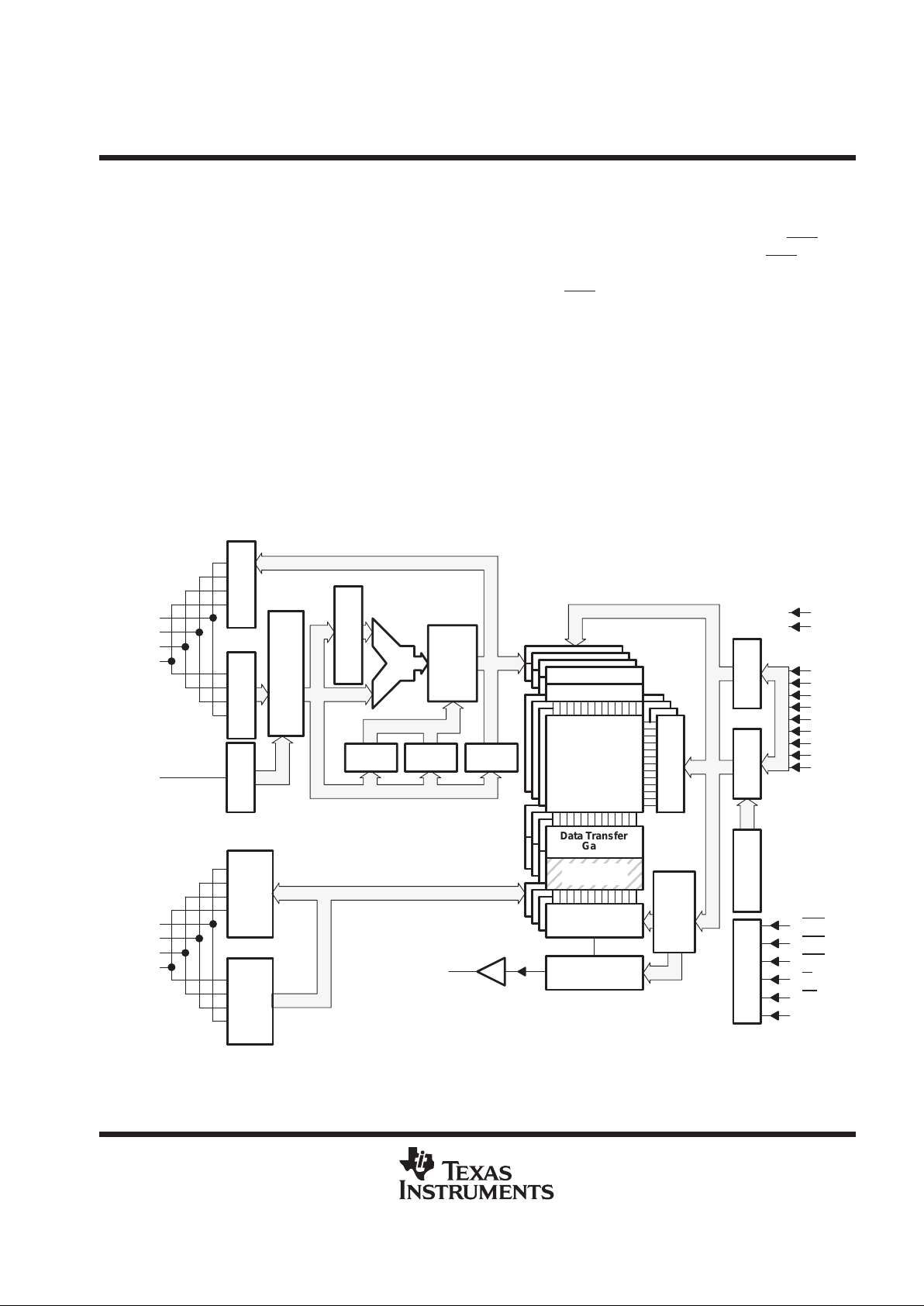
functional block diagram
Column Decoder
Sense Amplifier
Split Register
Data Transfer
Gate
Serial Data
Register
Serial Data
Pointer
W/B
Unlatch
W/B
Latch
Address
Mask
Write-
Per-Bit
Control
MUX
QSF
DQ0
DQ1
DQ2
DQ3
DSF
SDQ0
SDQ1
SDQ2
SDQ3
V
CC
A0
A1
A2
A3
A4
A5
A6
A7
A8
RAS
CAS
TRG
W
SC
SE
V
SS
O
u
t
p
u
t
B
u
f
f
e
r
I
n
p
u
t
B
u
f
f
e
r
I
n
p
u
t
B
u
f
f
e
r
S
p
e
c
i
a
l
F
u
n
c
t
i
o
n
L
o
g
i
c
S
e
r
i
a
l
O
u
t
p
u
t
B
u
f
f
e
r
C
o
l
o
r
R
e
g
i
s
t
e
r
S
e
r
i
a
l
I
n
p
u
t
B
u
f
f
e
r
R
o
w
D
e
c
o
d
e
r
C
o
l
u
m
n
B
u
f
f
e
r
R
o
w
B
u
f
f
e
r
R
e
f
r
e
s
h
C
o
u
n
t
e
r
T
i
m
i
n
g
G
e
n
e
r
a
t
o
r
S
e
r
i
a
l
A
d
d
r
e
s
s
C
o
u
n
t
e
r
Page 4
SMJ44C251B
262144 BY 4-BIT
MULTIPORT VIDEO RAM
SGMS058A – MARCH 1995 – REVISED JUNE 1995
4
POST OFFICE BOX 1443 • HOUSTON, TEXAS 77251–1443
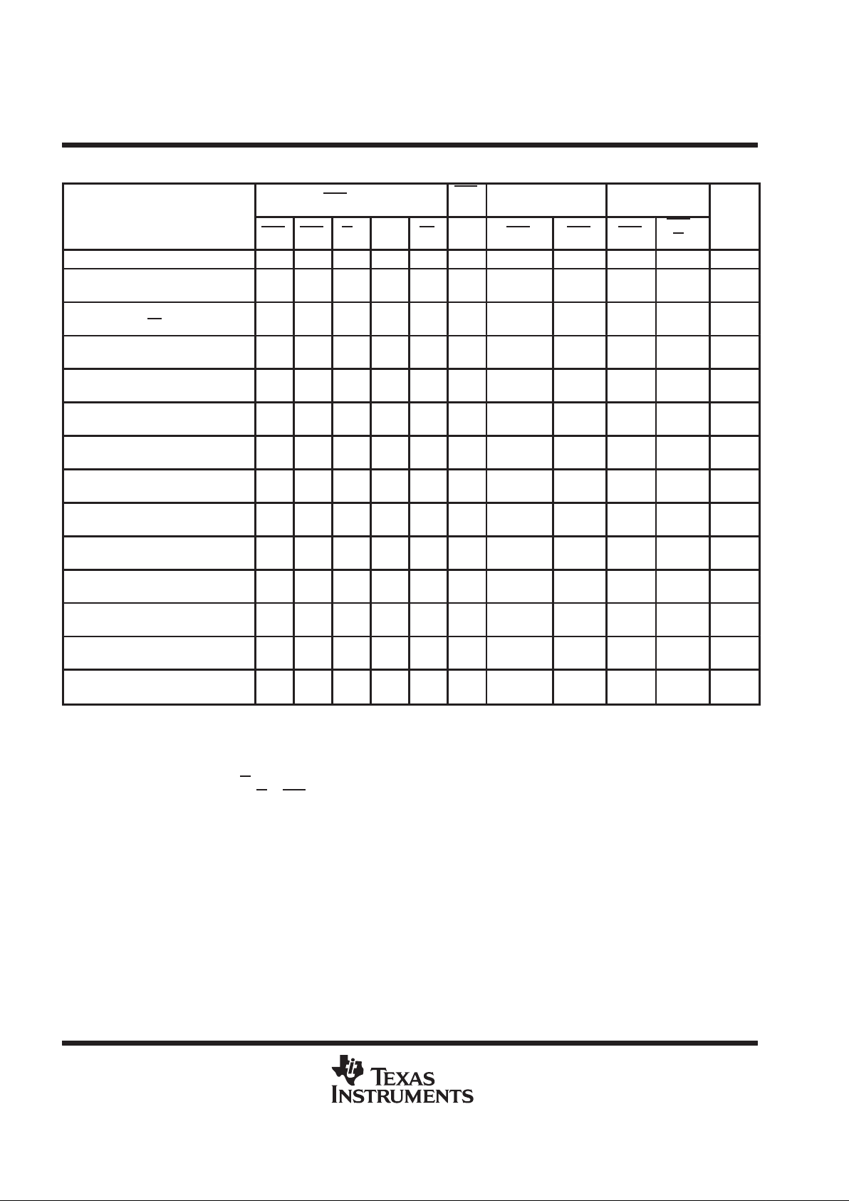
Function Table
RAS FALL
CAS
FALL
ADDRESS DQ0–DQ3
FUNCTION
CAS TRG W‡DSF SE DSF RAS CAS RAS
CAS
§
W
TYPE
†
CBR refresh L X X X X X X X X X R
Register-to-memory transfer
(transfer write)
H L L X L X
Row
Addr
Tap
Point
X X T
Alternate transfer write
(independent of SE
)
H L L H X X
Row
Addr
Tap
Point
X X T
Serial-write-mode enable
(pseudo-transfer write)
H L L L H X
Refresh
Addr
Tap
Point
X X T
Memory-to-register transfer
(transfer read)
H L H L X X
Row
Addr
Tap
Point
X X T
Split-register-transfer read
(must reload tap)
H L H H X X
Row
Addr
Tap
Point
X X T
Load and use write mask,
Write data to DRAM
H H L L X L
Row
Addr
Col
AddrDQMask
Valid
Data
R
Load and use write mask,
Block write to DRAM
H H L L X H
Row
Addr
Blk Addr
A2–A8DQMask
Col
Mask
R
Persistent write-per-bit,
Write data to DRAM
H H L H X L
Row
Addr
Col
Addr
X
Valid
Data
R
Persistent write-per-bit,
Block write to DRAM
H H L H X H
Row
Addr
Blk Addr
A2–A8
X
Col
Mask
R
Normal DRAM read/write
(nonmasked)
H H H L X L
Row
Addr
Col
Addr
X
Valid
Data
R
Block write to DRAM
(nonmasked)
H H H L X H
Row
Addr
Blk Addr
A2–A8
X
Col
Mask
R
Load write mask H H H H X L
Refresh
Addr
X X
DQ
Mask
R
Load color register H H H H X H
Refresh
Addr
X X
Color
Data
R
Legend:
H = High
L = Low
X = Don’t care
†
R = random access operation; T = transfer operation
‡
In persistent write-per-bit function, W
must be high during the refresh cycle.
§
DQ0–DQ3 are latched on the later of W
or CAS falling edge.
Col Mask = H: Write to address/column location enabled
DQ Mask = H: Write to I/O enabled
Page 5
SMJ44C251B
262144 BY 4-BIT
MULTIPORT VIDEO RAM
SGMS058A – MARCH 1995 – REVISED JUNE 1995
5
POST OFFICE BOX 1443 • HOUSTON, TEXAS 77251–1443
operation
Depending on the type of operation chosen, the signals of the SMJ44C251B perform different functions.
Table 1 summarizes the signal descriptions and the operational modes they control.
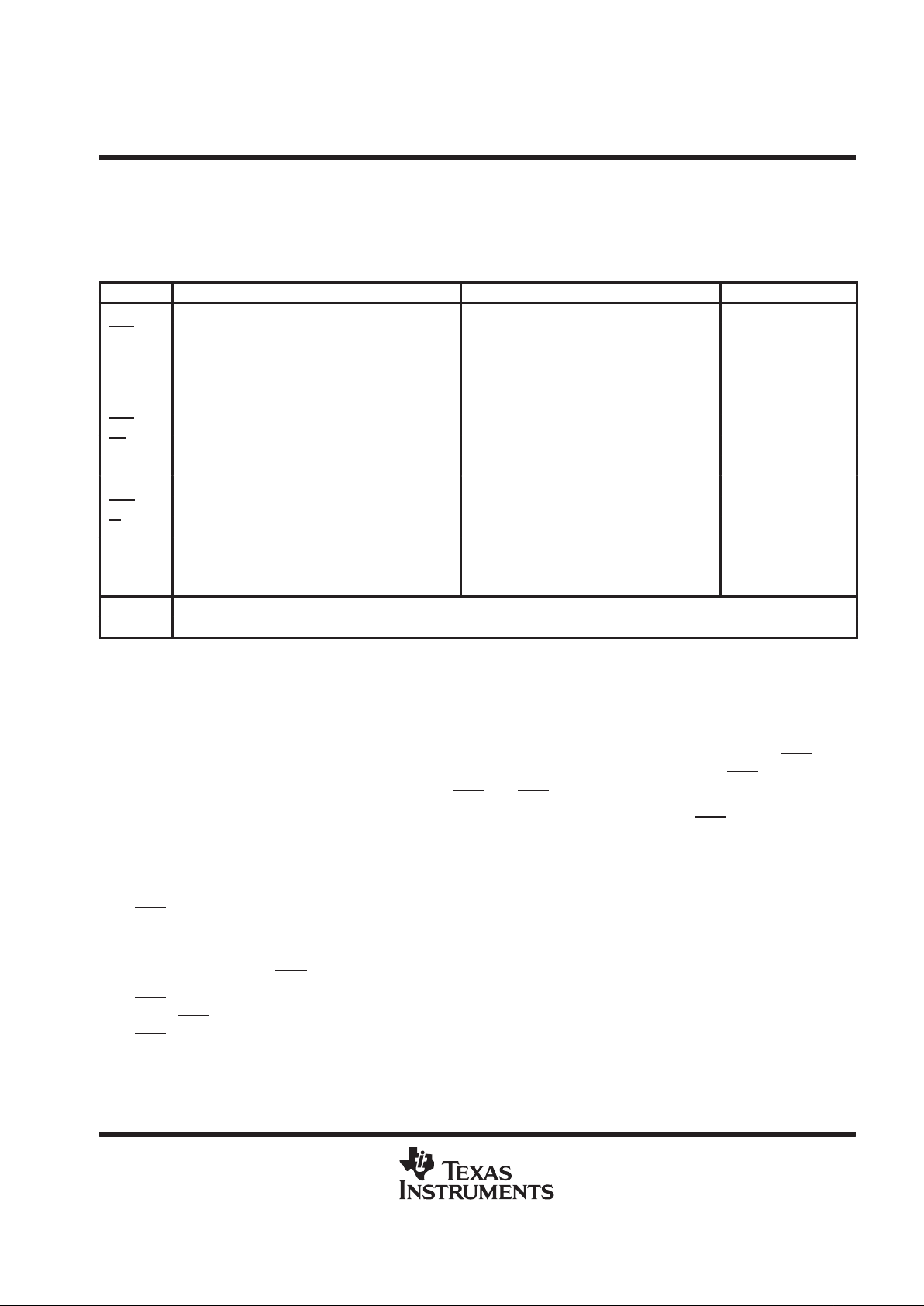
Table 1. Detailed Signal Description Versus Operational Mode
PIN DRAM TRANSFER SAM
A0–A8 Row, column address Row, tap address
CAS Column enable, output enable Tap-address strobe
DQi DRAM data I/O, write mask bits
DSF Block-write enable
Persistent write-per-bit enable
Color-register load enable
Split-register enable
Alternate write-transfer enable
RAS Row enable Row enable
SE Serial-in mode enable Serial enable
SC Serial clock
SDQ Serial-data I/O
TRG Q output enable Transfer enable
W Write enable, write-per-bit select Transfer-write enable
QSF
Split register
Active status
NC/GND Make no external connection or tie to system VSS.
V
CC
5-V supply (typical)
V
SS
Device ground
The SMJ44C251B has three kinds of operations: random-access operations typical of a DRAM, transfer
operations from memory arrays to the SAM, and serial-access operations through the SAM port. The signals
used to control these operations are described here, followed by discussions of the operations themselves.
address (A0–A8)
For DRAM operation, 18 address bits are required to decode one of the 262144 storage cell locations. Nine
row-address bits are set up on A0–A8 and latched onto the chip on the falling edge of RAS
. Nine
column-address bits are set up on A0–A8 and latched onto the chip on the falling edge of CAS
. All addresses
must be stable on or before the falling edges of RAS
and CAS.
During the transfer operation, the states of A0–A8 are latched on the falling edge of RAS
to select one of the
512 rows where the transfer occurs. T o select one of 512 tap points (starting positions) for the serial-data input
or output, the appropriate 9-bit column address (A0–A8) must be valid when CAS
falls.
row-address strobe (RAS
)
RAS
is similar to a chip enable because all DRAM cycles and transfer cycles are initiated by the falling edge
of RAS
. RAS is a control input that latches the states of row address, W, TRG, SE, CAS, and DSF onto the chip
to invoke DRAM and transfer functions.
column-address strobe (CAS
)
CAS
is a control input that latches the states of column address and DSF to control DRAM and transfer functions.
When CAS
is brought low during a transfer cycle, it latches the new tap point for the serial-data input or output.
CAS
also acts as an output enable for the DRAM outputs DQ0–DQ3.
Page 6

SMJ44C251B
262144 BY 4-BIT
MULTIPORT VIDEO RAM
SGMS058A – MARCH 1995 – REVISED JUNE 1995
6
POST OFFICE BOX 1443 • HOUSTON, TEXAS 77251–1443
output enable/transfer select (TRG)
TRG
selects either DRAM or transfer operation as RAS falls. For DRAM operation, TRG must be held high as
RAS
falls. During DRAM operation, TRG functions as an output enable for the DRAM outputs DQ0–DQ3. For
transfer operation, TRG
must be brought low before RAS falls.
write-mask select, write enable (W
)
In DRAM operation, W
enables data to be written to the DRAM. W is also used to select the DRAM write-per-bit
mode. Holding W
low on the falling edge of RAS invokes the write-per-bit operation. The SMJ44C251B supports
both the normal write-per-bit mode and the persistent write-per-bit mode.
For transfer operation, W
selects either a read-transfer operation (DRAM to SAM) or a write-transfer operation
(SAM to DRAM). During a transfer cycle, if W
is high when RAS falls, a read transfer occurs; if W is low, a write
transfer occurs.
special function select (DSF)
DSF is latched on the falling edge of RAS
or CAS, similar to an address. DSF determines which of the following
functions are invoked on a particular cycle:
D
Persistent write-per-bit
D
Block write
D
Split-register transfer read
D
Mask-register load for the persistent write-per-bit mode
D
Color-register load for the block-write mode
DRAM data I/O, write-mask data (DQ0–DQ3)
DRAM data is written via DQ terminals during a write or read-modify-write cycle. In an early-write cycle, W
is
brought low prior to CAS
and the data is strobed in by CAS with data setup and hold times referenced to this
signal. In a delayed-write or read-modify-write cycle, W
is brought low after CAS and the data is strobed in by
W
with data setup and hold times referenced to this signal.
The 3-state DQ output buffers provide direct TTL compatibility (no pullup resistors) with a fanout of two Series
54 TTL loads. Data out is the same polarity as data in. The outputs are in the high-impedance (floating) state
as long as CAS
and TRG are held high. Data does not appear at the outputs until both CAS and TRG are brought
low. Once the outputs are valid, they remain valid while CAS
and TRG are low. CAS or TRG going high returns
the outputs to the high-impedance state. In a register-transfer operation, the DQ outputs remain in the
high-impedance state for the entire cycle.
The write-per-bit mask is latched into the device via the random DQ terminals by the falling edge of RAS
. This
mask selects which of the four random I/Os are written.
serial data I/O (SDQ0–SDQ3)
Serial inputs and serial outputs share common I/O terminals. Serial-input or serial-output mode is determined
by the previous transfer cycle. If the previous transfer cycle was a read transfer, the data register is in
serial-output mode. While in serial-output mode, data in SAM is accessed from the least significant bit to the
most significant bit. The data registers operate modulo 512; so after bit 511 is accessed, the next bits to be
accessed are 00, 01, 02, etc. If the previous transfer cycle was either a write transfer or a pseudo transfer, the
data register is in serial-input mode and signal data can be input to the register.
serial clock (SC)
Serial data is accessed in or out of the data register on the rising edge of SC. The SMJ44C251B is designed
to work with a wide range of clock-duty cycles to simplify system design. There is no refresh requirement
because the data registers that comprise the SAM are static. There is also no minimum SC clock operating
frequency.
Page 7

SMJ44C251B
262144 BY 4-BIT
MULTIPORT VIDEO RAM
SGMS058A – MARCH 1995 – REVISED JUNE 1995
7
POST OFFICE BOX 1443 • HOUSTON, TEXAS 77251–1443
serial enable (SE)
During serial-access operations SE
is used as an enable/disable for SDQ in both the input and output modes.
If SE
is held as RAS falls during a write-transfer cycle, a pseudo-transfer write occurs. There is no actual transfer,
but the data register switches from the output mode to the input mode.
no connect/ground (NC/GND)
NC/GND is reserved for the manufacturer’s test operation. It is an input and should be tied to system ground
or left floating for proper device operation.
special function output (QSF)
During split-register operation the QSF output indicates which half of the SAM is being accessed. When QSF
is low, the serial-address pointer is accessing the lower (least significant) 256 bits of SAM. When QSF is high,
the serial-address pointer is accessing the higher (most significant) 256 bits of SAM. QSF changes state upon
crossing the boundary between the two SAM halves in the split-register mode.
During normal transfer operations QSF changes state upon completing a transfer cycle. This state is determined
by the tap point being loaded during the transfer cycle.
power up
T o achieve proper device operation, an initial pause of 200 µs is required after power-up, followed by a minimum
of eight RAS
cycles or eight CBR cycles, a memory-to-register transfer cycle, and two SC cycles.
Page 8
SMJ44C251B
262144 BY 4-BIT
MULTIPORT VIDEO RAM
SGMS058A – MARCH 1995 – REVISED JUNE 1995
8
POST OFFICE BOX 1443 • HOUSTON, TEXAS 77251–1443
random-access operation
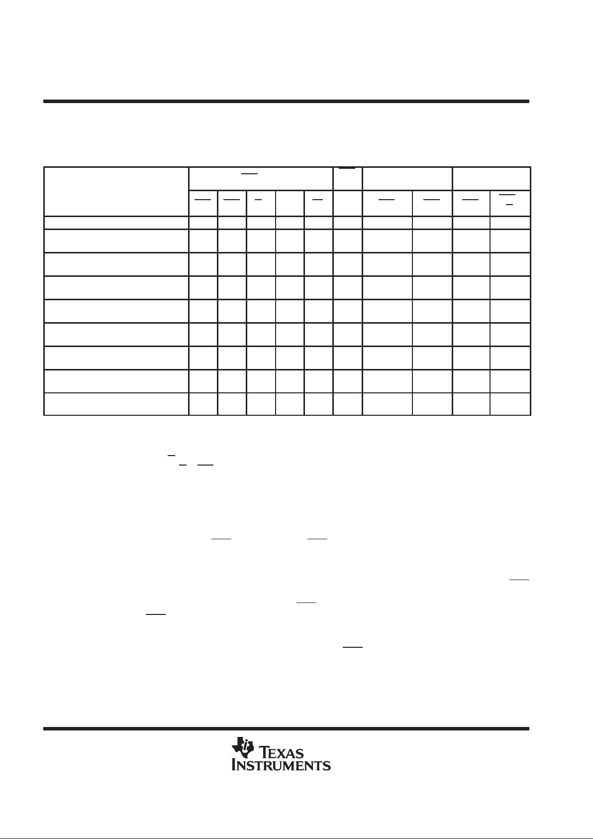
The random-access operation functions are summarized in Table 2 and described in the following sections.
Table 2. Random-Access-Operation Functions
RAS FALL
CAS
FALL
ADDRESS DQ0–DQ3
FUNCTION
CAS TRG W†DSF SE DSF RAS CAS RAS
CAS
‡
W
CBR refresh L X X X X X X X X X
Load and use write mask,
Write data to DRAM
H H L L X L
Row
Addr
Col
Addr
DQ
Mask
Valid
Data
Load and use write mask,
Block write to DRAM
H H L L X H
Row
Addr
Blk Addr
A2–A8DQMask
Col
Mask
Persistent write-per-bit,
Write data to DRAM
H H L H X L
Row
Addr
Col
Addr
X
Valid
Data
Persistent write-per-bit,
Block write to DRAM
H H L H X H
Row
Addr
Blk Addr
A2–A8
X
Col
Mask
Normal DRAM read/write
(nonmasked)
H H H L X L
Row
Addr
Col
Addr
X
Valid
Data
Block write to DRAM
(nonmasked)
H H H L X H
Row
Addr
Blk Addr
A2–A8
X
Col
Mask
Load write mask H H H H X L
Refresh
Addr
X X
DQ
Mask
Load color register H H H H X H
Refresh
Addr
X X
Color
Data
Legend:
H = High
L = Low
X = Don’t care
†
In persistent write-per-bit function, W
must be high during the refresh cycle.
‡
DQ0–DQ3 are latched on the later of W
or CAS falling edge.
Col Mask = H: Write to address/column location enabled
DQ Mask = H: Write to I/O enabled
enhanced page mode
Enhanced page-mode operation allows faster memory access by keeping the same row address while selecting
random column addresses. This mode eliminates the time required for row address setup-and-hold and
address multiplex. The maximum RAS
low time and the CAS page cycle time used determine the number of
columns that can be accessed.
Unlike conventional page-mode operation, the enhanced page mode allows the SMJ44C251B to operate at a
higher data bandwidth. Data retrieval begins as soon as the column address is valid rather than when CAS
transitions low. A valid column address can be presented immediately after row-address hold time has been
satisfied, usually well in advance of the falling edge of CAS
. In this case, data can be obtained after t
a(C)
max
(access time from CAS
low), if t
a(CA)
max (access time from column address) has been satisfied.
refresh
There are three types of refresh available on the SMJ44C251B: RAS-only refresh, CBR refresh, and hidden
refresh.
Page 9

SMJ44C251B
262144 BY 4-BIT
MULTIPORT VIDEO RAM
SGMS058A – MARCH 1995 – REVISED JUNE 1995
9
POST OFFICE BOX 1443 • HOUSTON, TEXAS 77251–1443
RAS-only refresh
A refresh operation must be performed to each row at least once every 8 ms to retain data. Unless CAS is
applied, the output buffers are in the high-impedance state, so the RAS
-only refresh sequence avoids any
output during refresh. Externally generated addresses must be supplied during RAS
-only refresh. Strobing each
of the 512 row addresses with RAS
causes all bits in each row to be refreshed. CAS can remain high (inactive)
for this refresh sequence to conserve power.
CAS-before-RAS (CBR) refresh
CBR refresh is accomplished by bringing CAS low earlier than RAS. The external row address is ignored and
the refresh row address is generated internally when using CBR refresh. Other cycles can be performed in
between CBR cycles without disturbing the internal address generation.
hidden refresh
A hidden refresh is accomplished by holding CAS low in the DRAM-read cycle and cycling RAS. The output data
of the DRAM-read cycle remains valid while the refresh is being carried out. Like the CBR refresh, the refreshed
row addresses are generated internally during the hidden refresh.
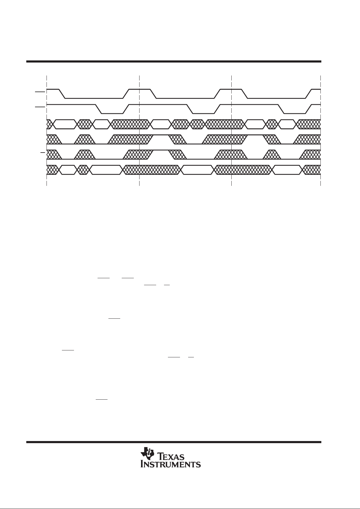
write-per-bit
The write-per-bit feature allows masking of any combination of the four DQs on any write cycle (see Figure 1).
The write-per-bit operation is invoked only when W
is held low on the falling edge of RAS. If W is held high on
the falling edge of RAS
, write-per-bit is not enabled and the write operation is performed to all four DQs. The
SMJ44C251B offers two write-per-bit modes: the nonpersistent write-per-bit mode and the persistent
write-per-bit mode.
nonpersistent write-per-bit
When DSF is low on the falling edge of RAS, the write mask is reloaded. A 4-bit code (the write-per-bit mask)
is input to the device via the random DQ terminals and latched on the falling edge of RAS
. The write-per-bit mask
selects which of the four random I/Os are written and which are not. After RAS
has latched the on-chip
write-per-bit mask, input data is driven onto the DQ terminals and is latched on the later falling edge of CAS
or
W
. When a data low is strobed into a particular I/O on the falling edge of RAS, data is not written to that I/O. When
a data high is strobed into a particular I/O on the falling edge of RAS
, data is written to that I/O.
persistent write-per-bit
When DSF is high on the falling edge of RAS, the write-per-bit mask is not reloaded: it retains the value stored
during the last write-per-bit mask reload. This mode of operation is known as persistent write-per-bit because
the write-per-bit mask is persistent over an arbitrary number of write cycles. The write-per-bit mask reload can
be done during the nonpersistent write-per-bit cycle or by the mask-register-load cycle.
Page 10
SMJ44C251B
262144 BY 4-BIT
MULTIPORT VIDEO RAM
SGMS058A – MARCH 1995 – REVISED JUNE 1995
10
POST OFFICE BOX 1443 • HOUSTON, TEXAS 77251–1443
persistent write-per-bit (continued)
RAS
CAS
A0–A8
DSF
W
DQ0–
DQ3
Nonpersistant Write-Per-Bit
DQ Mask = H: Write to I/O enabled
= L: Write to I/O disabled
Write-Mask-Register Load Persistent Write-Per-Bit
DQ Mask Write DataDQ Mask Write Data
Figure 1. Example of Write-Per-Bit Operations
block write
The block-write mode allows data (present in an on-chip color register) to be written into four consecutive
column-address locations. The 4-bit color register is loaded by the color-register-load cycle. Both write-per-bit
modes can be applied in the block-write cycle. The block-write mode also offers the 4 × 4 column-mask
capability.
load color register
The load-color-register cycle is performed using normal DRAM write-cycle timing except that DSF is held high
on the falling edges of RAS
and CAS. A 4-bit code is input to the color register via the random I/O terminals and
latched on the later of the falling edge of CAS
or W. After the color register is loaded, it retains data until power
is lost or until another load-color-register cycle is executed.
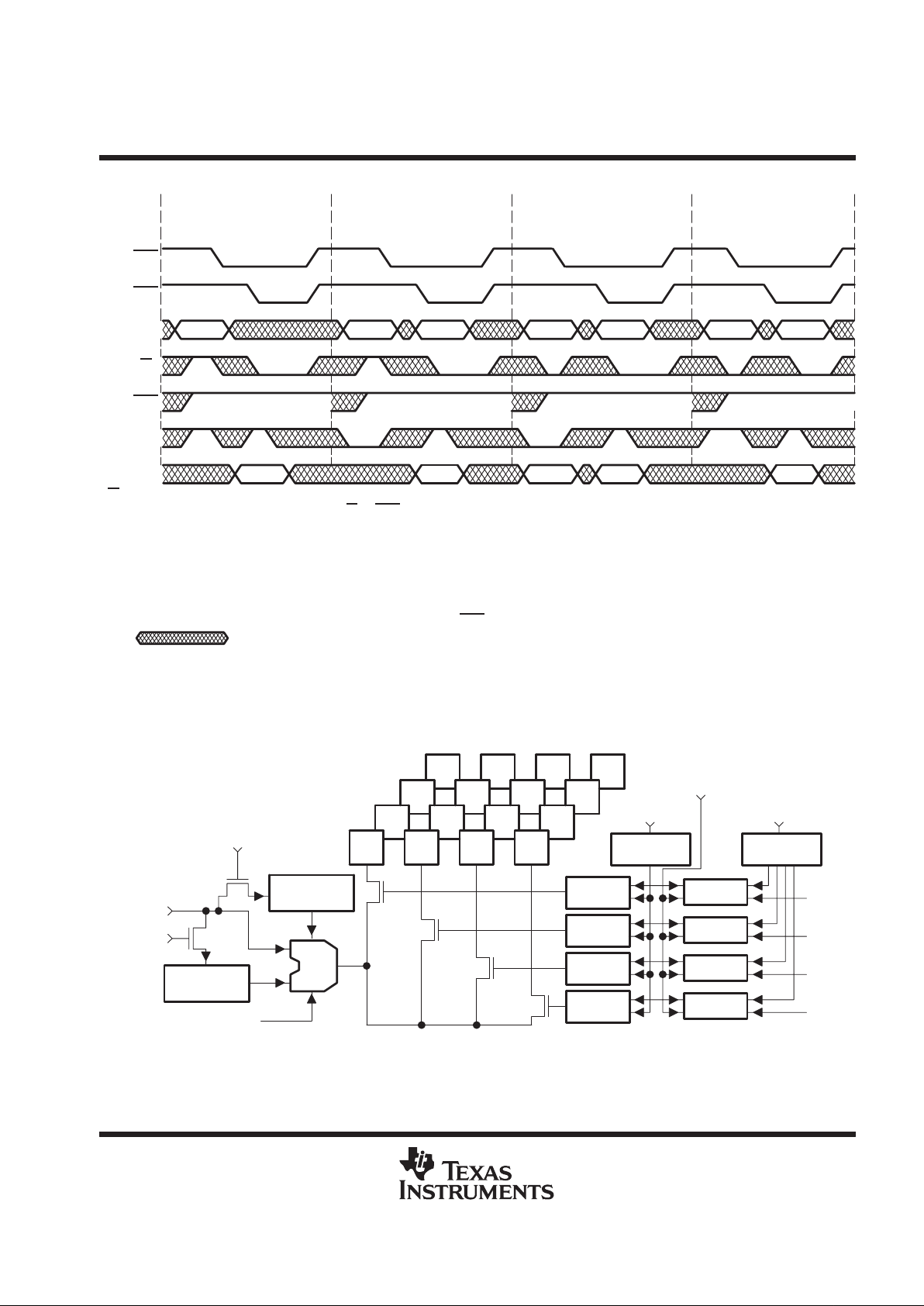
block write cycle
After the color register is loaded, the block-write cycle can begin as a normal DRAM write cycle with DSF held
high on the falling edge of CAS
(see Figures 2, 3, and 4). When the block-write cycle is invoked, each data bit
in the 4-bit color register is written to selected bits of the four adjacent columns of the corresponding random
I/O.
During block-write cycles, only the seven most significant column addresses (A2–A8) are latched on the falling
edge of CAS
. The two least significant addresses (A0–A1) are replaced by four DQ bits (DQ0–DQ3), which
are also latched on the later of the falling edge of CAS
or W. These four bits are used as a column mask, and
they indicate which of the four column-address locations addressed by A2–A8 are written with the contents of
the color register during the block-write cycle. DQ0 enables a write to column-address A1 = 0 (low), A0 = 0 (low);
DQ1 enables a write to column-address A1 = 0 (low), A0 = 1 (high); DQ2 enables a write to column-address
A1 = 1 (high), A0 = 0 (low); DQ3 enables a write to column-address A1 = 1 (high), A0 = 1 (high). A high logic
level enables a write, and a low logic level disables the write. A maximum of 16 bits (4 × 4) can be written to
memory during each CAS
cycle in the block-write mode.
Page 11
SMJ44C251B
262144 BY 4-BIT
MULTIPORT VIDEO RAM
SGMS058A – MARCH 1995 – REVISED JUNE 1995
11
POST OFFICE BOX 1443 • HOUSTON, TEXAS 77251–1443
block write cycle (continued)
12323 2
3
4 5 65
5
Load-Color-Register Cycle Block-Write Cycle
†
(no DQ mask)
Block-Write Cycle
†
(load and use DQ mask)
Block-Write Cycle
†
(use previously
loaded DQ mask)
RAS
CAS
A0–A8
W
†
TRG
DSF
DQ0–DQ3
†
W must be low during the block-write cycle.
NOTE: DQ0–DQ3 are latched on the later of W
or CAS falling edge except in block 6 (see legend).
Legend:
1. Refresh address
2. Row address
3. Block address (A2 –A8)
4. Color-register data
5. Column-mask data
6. DQ-mask data. DQ0–DQ3 are latched on the falling edge of RAS
.
= don’t care
Figure 2. Example Block-Write Diagram Operations
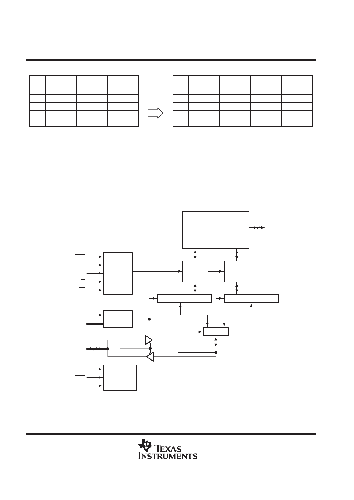
N
DQ0
DQ
Write-Mask
Register
N + 1
N + 2 N + 3
I/O3
I/O2
I/O1
I/O0
Block-Write
Enable
Load
Color
Register
DQ1
DQ2
DQ3
MUX
MUX
MUX
MUX
4-of-512
Decode
1-of-4
Decode
A2–A8
Write
Select
Write
Select
Write
Select
Write
Select
Color
Register
Load Write
Mask
Write
Enable
Data
In
MUX
Block-Write
Enable
A0–A1
Figure 3. Block-Write Circuit Block Diagram
Page 12
SMJ44C251B
262144 BY 4-BIT
MULTIPORT VIDEO RAM
SGMS058A – MARCH 1995 – REVISED JUNE 1995
12
POST OFFICE BOX 1443 • HOUSTON, TEXAS 77251–1443
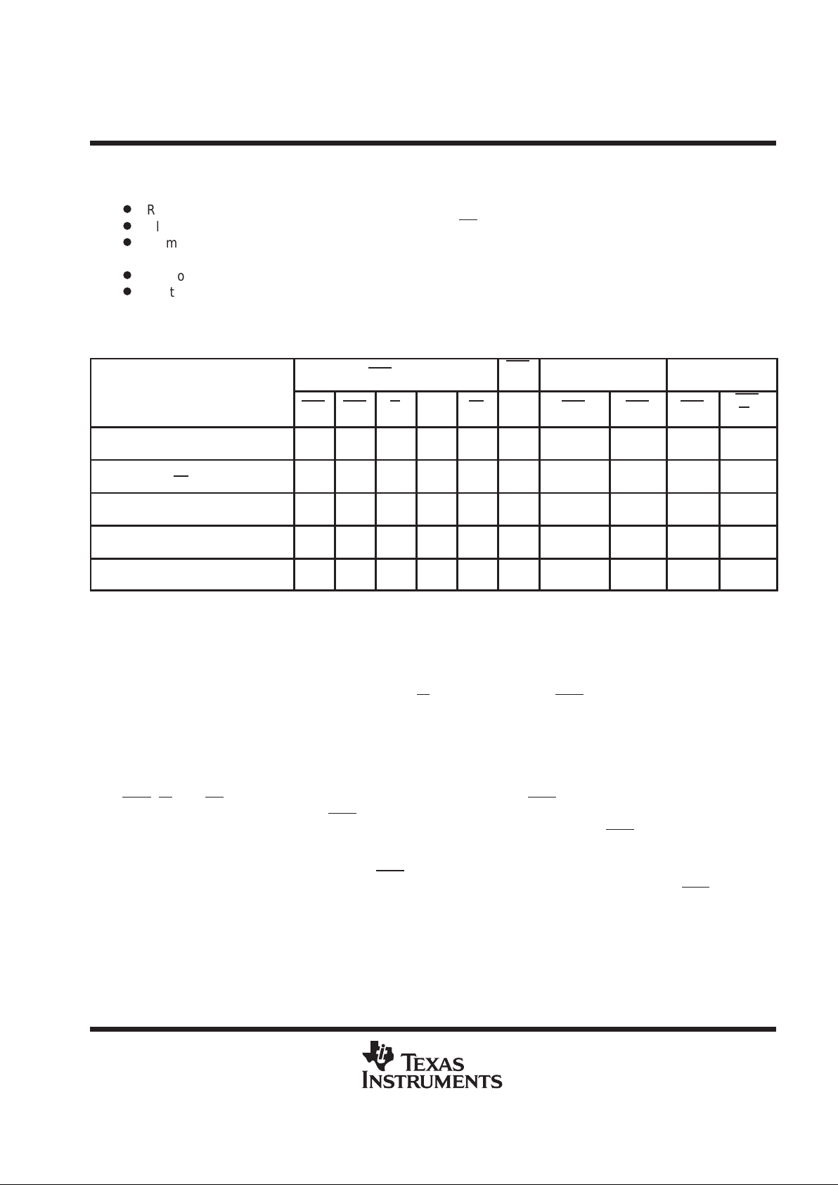
block write cycle (continued)
DQ MASK
COLUMN
MASK
COLOR
REGISTER
DATA
COLUMN 1 COLUMN 2 COLUMN 3 COLUMN 4
DQ0 1 0 0 DQ0 Masked 0 0 0
DQ1 1 1 0
Block Write
DQ1 Masked 0 0 0
DQ2 0 1 1 DQ2 Masked Masked Masked Masked
DQ3 1 1 1 DQ3 Masked 1 1 1
Figure 4. Example of Block Write Operation With DQ Mask and Address Mask
transfer operation
Transfer operations between the memory arrays (DRAM) and the data registers (SAM) are invoked by bringing
TRG
low before RAS falls. The states of W, SE, and DSF, which are also latched on the falling edge of RAS,
determine which transfer operation is invoked. Figure 5 shows an overview of data flow between the random
and the serial interfaces.
DQ0–DQ3
Col
511
Col
0
Random-Access Port
Row
0
Row
511
256
256-Bit Data Register
Transfer-
Control
Logic
Serial
Counter
Serial-
I/O
Control
TRG
A8
DSF
W
SE
Transfer-
Pass
Gate
Col
255
Col
256
Memory Array
262 144 Bits
256
Transfer-
Pass
Gate
SC
A0–A8
A8
SDQ0–SDQ3
256 256
256-Bit Data Register
MUX
SE
TRG
W
4
4
Figure 5. Block Diagram Showing One Random and One Serial-I/O Interface
Page 13
SMJ44C251B
262144 BY 4-BIT
MULTIPORT VIDEO RAM
SGMS058A – MARCH 1995 – REVISED JUNE 1995
13
POST OFFICE BOX 1443 • HOUSTON, TEXAS 77251–1443
transfer operation (continued)
As shown in Table 3, the SMJ44C251B supports five basic modes of transfer operation:
D
Register-to-memory transfer (normal write transfer, SAM to DRAM)
D
Alternate-write transfer (independent of the state of SE)
D
Memory-to-register transfer (pseudo-transfer write). Switches serial port from serial-out mode to serial-in
mode. No actual data transfer takes place between the DRAM and the SAM.
D
Memory-to-register transfer (normal-read transfer, transfer entire contents of DRAM row to SAM)
D
Split-register-read transfer (divides the SAM into a low and a high half. Only one half is transferred to the
SAM while the other half is read from the serial I/O port.)
Table 3. Transfer-Operation Functions
RAS FALL
CAS
FALL
ADDRESS DQ0–DQ3
FUNCTION
CAS TRG W DSF SE DSF RAS CAS RAS
CAS
W
Register-to-memory transfer
(normal write transfer)
H L L X L X
Row
Addr
Tap
Point
X X
Alternate-write transfer
(independent of SE
)
H L L H X X
Row
Addr
Tap
Point
X X
Serial-write-mode enable
(pseudo-transfer write)
H L L L H X
Refresh
Addr
Tap
Point
X X
Memory-to-register transfer
(normal read transfer)
H L H L X X
Row
Addr
Tap
Point
X X
Split-register-read transfer
(must reload tap)
H L H H X X
Row
Addr
Tap
Point
X X
Legend:
H = High
L = Low
X = Don’t care
write transfer
All write-transfer cycles (except the pseudo write transfer) transfer the entire content of SAM to the selected row
in the DRAM. To invoke a write-transfer cycle, W
must be low when RAS falls. There are three possible
write-transfer operations: normal-write transfer, alternate-write transfer, and pseudo-write transfer.
All write-transfer cycles switch the serial port to the serial-in mode.
normal-write transfer (SAM-to-DRAM transfer)
A normal-write transfer cycle loads the contents of the serial-data register to a selected row in the memory array .
TRG
, W, and SE are brought low and latched at the falling edge of RAS. Nine row-address bits (A0–A8) are
also latched at the falling edge of RAS
to select one of the 512 rows available as the destination of the data
transfer. The nine column-address bits (A0–A8) are latched at the falling edge of CAS
to select one of the 512
tap points in SAM that are available for the next serial input.
During a write-transfer operation before RAS
falls, the serial-input operation must be suspended after a
minimum delay of t
d(SCRL)
but can be resumed after a minimum delay of t
d(RHSC)
after RAS goes high
(see Figure 6).
Page 14
SMJ44C251B
262144 BY 4-BIT
MULTIPORT VIDEO RAM
SGMS058A – MARCH 1995 – REVISED JUNE 1995
14
POST OFFICE BOX 1443 • HOUSTON, TEXAS 77251–1443
normal-write transfer (SAM-to-DRAM transfer) (continued)
RAS
CAS
A0–A8
TRG
W
SE
t
d(SCRL)
t
d(RHSC)
SC
Row Tap Point
Figure 6. Normal-Write-Transfer-Cycle Timing
alternate-write transfer (refer to Figure 30)
When DSF is brought high and latched at the falling edge of RAS in the normal-write-transfer cycle, the
alternate-write transfer occurs.
pseudo-write transfer (write-mode control) (refer to Figure 28)
T o invoke the pseudo-write transfer (write-mode control cycle), SE is brought high and latched at the falling edge
of RAS
. The pseudo-write transfer does not actually invoke any data transfer but switches the mode of the serial
port from the serial-out (read) mode to the serial-in (write) mode.
Before serial data can be clocked into the serial port via the SDQ terminals and the SC input, the SDQ terminals
must be switched into input mode. Because the transfer does not occur during the pseudo-transfer write, the
row address (A0–A8) is in the don’t care state and the column address (A0–A8), which is latched on the falling
edge of CAS
, selects one of the 512 tap points in the SAM that are available for the next serial input.
read transfer (DRAM-to-SAM transfer) (refer to Figure 7)
During a read-transfer cycle, data from the selected row in DRAM is transferred to SAM. There are two
read-transfer operations: normal-read transfer and split-register-read transfer.
normal-read transfer
(refer to
Figure 7
)
The normal-read-transfer operation loads data from a selected row in DRAM into SAM. TRG is brought low and
latched at the falling edge of RAS
. Nine row-address bits (A0–A8) are also latched at the falling edge of RAS
to select one of the 512 rows available for transfer. The nine column-address bits (A0–A8) are latched at the
falling edge of CAS
to select one of the SAM’s 512 available tap points where the serial data is read out.
A normal-read transfer can be performed in three ways: early-load read transfer, real-time or midline-load read
transfer, and late-load read transfer. Each of these offers the flexibility of controlling the TRG
trailing edge in
the read-transfer cycle (see Figure 7).
Page 15
SMJ44C251B
262144 BY 4-BIT
MULTIPORT VIDEO RAM
SGMS058A – MARCH 1995 – REVISED JUNE 1995
15
POST OFFICE BOX 1443 • HOUSTON, TEXAS 77251–1443
normal-read transfer (continued)
Row Tap Point Row Tap Point Row Tap Point
Bit
512
Tap
Bit
Bit
510
Bit
511
Tap
Bit
Bit
510
Bit
511
Tap
Bit
Early-Load Read Transfer Real-Time-Reload Read T ransfer Late-Load Read Transfer
RAS
CAS
A0–A8
TRG
SC
Figure 7. Normal-Read-Transfer Timings
split-register-read transfer
In split-register-read-transfer operation, the serial-data register is split into halves. The low half contains bits
0–255, and the high half contains 256–511. While one half is being read out of the SAM port, the other half can
be loaded from the memory array.
T o invoke a split-register read-transfer cycle, DSF is brought high, TRG
is brought low, and both are latched at
the falling edge of RAS
. Nine row-address bits (A0–A8) are also latched at the falling edge of RAS to select
one of the 512 rows available for the transfer. The nine column-address bits (A0–A8) are latched at the falling
edge of CAS
, where address bits A0–A7 select one of the 255 tap points in the specified half of SAM and
address bit A8 selects which half is to be transferred. If A8 is a logic low, the low half is transferred. If A8 is a
logic high, the high half is transferred. SAM locations 255 and 511 cannot be used as tap points.
A normal-read transfer must precede the split-register-read transfer to ensure proper operation. After the
normal-read-transfer cycle, the first split-register read transfer can follow immediately without any minimum SC
requirement. However, there is a minimum requirement of a rising edge of SC between split-register
read-transfer cycles.
QSF indicates which half of the SAM is being accessed during serial-access operation. When QSF is low, the
serial-address pointer is accessing the lower (least significant) 256 bits of the SAM. When QSF is high, the
pointer is accessing the higher (most significant) 256 bits of the SAM. QSF changes state upon completing a
normal-read-transfer cycle. The tap point loaded during the current transfer cycle determines the state of QSF .
In split-register read-transfer mode, QSF changes state when a boundary between the two register halves is
reached (see Figure 8 and Figure 9).
Page 16
SMJ44C251B
262144 BY 4-BIT
MULTIPORT VIDEO RAM
SGMS058A – MARCH 1995 – REVISED JUNE 1995
16
POST OFFICE BOX 1443 • HOUSTON, TEXAS 77251–1443
split-register-read transfer (continued)
RAS
CAS
DSF
TRG
QSF
SC
Tap
Point N
t
d(GHQSF)
Read Transfer
With Tap Point N
t
d(CLQSF)
Split-Register
Read Transfer
Figure 8. Example of a Split-Register Read-Transfer Cycle After a Normal Read-Transfer Cycle
255
or 511
t
a(SCQSF)
RAS
CAS
DSF
TRG
QSF
SC
Tap
Point N
Split-Register
Read Transfer
With Tap Point N
Split-Register
Read Transfer
t
d(MSRL)
t
d(RHMS)
Figure 9. A Split-Register Read-Transfer Cycle After a Split-Register Read-Transfer Cycle
Page 17

SMJ44C251B
262144 BY 4-BIT
MULTIPORT VIDEO RAM
SGMS058A – MARCH 1995 – REVISED JUNE 1995
17
POST OFFICE BOX 1443 • HOUSTON, TEXAS 77251–1443
serial-access operation
The serial-read and serial-write operations can be performed through the SAM port simultaneously and
asynchronously with DRAM operations except during transfer operations. The preceding transfer operation
determines the input or output state of the SAM port. If the preceding transfer operation is a read-transfer
operation, the SAM port is in the output mode. If the preceding transfer operation is a write- or
pseudo-write-transfer operation, the SAM port is in the input mode.
Serial data can be read out of or written into SAM by clocking SC starting at the tap point loaded by the preceding
transfer cycle, proceeding sequentially to the most significant bit (bit 511), then wrapping around to the least
significant bit (bit 0) (see Figure 10).
511510Tap210
Figure 10. Serial Pointer Direction for Serial Read/Write
For split-register read-transfer operation, serial data can be read out from the active half of SAM by clocking
SC starting at the tap point loaded by the preceding split-register-transfer cycle, then proceeding sequentially
to the most significant bit of the half, bit 255 or bit 51 1. If there is a split-register-read transfer to the inactive half
during this period, the serial pointer points next to the tap-point location loaded by that split register (see
Figure 11, Case I). If there is no split-register read transfer to the inactive half during this period, the serial pointer
points next to bit 256 or bit 0, respectively (see Figure 11, Case II).
255254Tap0 511510Tap256
Case I
255254Tap0 511510Tap256
Case I I
Figure 11. Serial Pointer for Split-Register Read
Page 18

SMJ44C251B
262144 BY 4-BIT
MULTIPORT VIDEO RAM
SGMS058A – MARCH 1995 – REVISED JUNE 1995
18
POST OFFICE BOX 1443 • HOUSTON, TEXAS 77251–1443
absolute maximum ratings over operating free-air temperature range (unless otherwise noted)
†
Supply voltage range, V
CC
(see Note 1) –1 V to 7 V. . . . . . . . . . . . . . . . . . . . . . . . . . . . . . . . . . . . . . . . . . . . . . . .
Voltage range on any pin (see Note 1) –1 V to 7 V. . . . . . . . . . . . . . . . . . . . . . . . . . . . . . . . . . . . . . . . . . . . . . . . . .
Short-circuit output current 50 mA. . . . . . . . . . . . . . . . . . . . . . . . . . . . . . . . . . . . . . . . . . . . . . . . . . . . . . . . . . . . . . . .
Power dissipation 1 W. . . . . . . . . . . . . . . . . . . . . . . . . . . . . . . . . . . . . . . . . . . . . . . . . . . . . . . . . . . . . . . . . . . . . . . . . .
Operating free-air temperature range, T
A
: L suffix 0°C to 70°C. . . . . . . . . . . . . . . . . . . . . . . . . . . . . . . . . . . . . .
M suffix – 55°C to 125°C. . . . . . . . . . . . . . . . . . . . . . . . . . . . . . . . .
Storage temperature range, T
stg
–65°C to 150°C. . . . . . . . . . . . . . . . . . . . . . . . . . . . . . . . . . . . . . . . . . . . . . . . . . .
†
Stresses beyond those listed under “absolute maximum ratings” may cause permanent damage to the device. These are stress ratings only, and
functional operation of the device at these or any other conditions beyond those indicated under “recommended operating conditions” is not
implied. Exposure to absolute-maximum-rated conditions for extended periods may affect device reliability.
NOTE 1: All voltage values are with respect to VSS.
recommended operating conditions
MIN NOM MAX UNIT
V
CC
Supply voltage 4.5 5 5.5 V
V
SS
Supply voltage 0 V
V
IH
High-level input voltage 2.9 6.5 V
V
IL
Low-level input voltage (see Note Note 2) –1 0.6 V
p
p
L suffix 0 70
°
TAOperating free-air temperature
M suffix – 55 125
°C
p
p
L suffix 70
°
TCOperating case temperature
M suffix 125
°C
NOTE 2: The algebraic convention, where the more negative (less positive) limit is designated as minimum, is used for logic-voltage levels only.
Page 19

SMJ44C251B
262144 BY 4-BIT
MULTIPORT VIDEO RAM
SGMS058A – MARCH 1995 – REVISED JUNE 1995
19
POST OFFICE BOX 1443 • HOUSTON, TEXAS 77251–1443
electrical characteristics over recommended ranges of supply voltage and operating free-air
temperature (unless otherwise noted)
PARAMETER TEST CONDITIONS MIN MAX UNIT
V
OH
High-level output voltage IOH = –5 mA 2.4 V
V
OL
Low-level output voltage (see Note 3) IOL = 4.2 mA 0.4 V
I
I
Input leakage current
VCC = 5 V, VI = 0 V to 5.8 V,
All others open
±10 µA
I
O
Output leakage current (see Note 4) VCC = 5.5 V, VO = 0 V to V
CC
±10 µA
NOTES: 3. The SMJ44C251B may exhibit simultaneous switching noise as described in the Texas Instruments
Advanced CMOS Logic
Designer’s Handbook
. This phenomenon is exhibited on the DQ terminals when the SDQ terminals are switched and on the SDQ
terminals when the DQ terminals are switched. This may cause VOL and VOH to exceed the data-book limit for a short period of time,
depending upon output loading and temperature. Care should be taken to provide proper termination, decoupling, and layout of the
device to minimize simultaneous switching effects.
4. SE
is disabled for SDQ output leakage tests.
electrical characteristics over recommended ranges of supply voltage and operating free-air
temperature (unless otherwise noted)
SAM
’44C251B-10 ’44C251B-12
PARAMETER (SEE NOTE 5)
TEST CONDITIONS
†
PORT
MIN MAX MIN MAX
UNIT
I
CC1
Operating current t
c(rd)
and t
c(W)
= MIN Standby 100 90
I
CC1A
Operating current t
c(SC)
= MIN Active 110 100
I
CC2
Standby current All clocks = V
CC
Standby 15 15
I
CC2A
Standby current t
c(SC)
= MIN Active 35 35
I
CC3
RAS-only refresh current t
c(rd)
and t
c(W)
= MIN Standby 100 90
I
CC3A
RAS-only refresh current t
c(SC)
= MIN Active 110 100
I
CC4
Page-mode current t
c(P)
= MIN Standby 65 60
mA
I
CC4A
Page-mode current t
c(SC)
= MIN Active 70 65
I
CC5
CAS-before-RAS current t
c(rd)
and t
c(W)
= MIN Standby 90 80
I
CC5A
CAS-before-RAS current t
c(SC)
= MIN Active 110 100
I
CC6
Data-transfer current t
c(rd)
and t
c(W)
= MIN Standby 100 90
I
CC6A
Data-transfer current t
c(SC)
= MIN Active 110 100
†
For conditions shown as MIN/MAX, use the appropriate value specified in the timing requirements.
NOTE 5: ICC (standby) denotes that the SAM port is inactive (standby) and the DRAM port is active (except for I
CC2
).
I
CCA
(active) denotes that the SAM port is active and the DRAM port is active (except for I
CC2
).
ICC is measured with no load on DQ or SDQ.
Page 20

SMJ44C251B
262144 BY 4-BIT
MULTIPORT VIDEO RAM
SGMS058A – MARCH 1995 – REVISED JUNE 1995
20
POST OFFICE BOX 1443 • HOUSTON, TEXAS 77251–1443
capacitance over recommended ranges of supply voltage and operating free-air temperature,
f = 1 MHz (see Note 6)
PARAMETER MIN MAX UNIT
C
i(A)
Input capacitance, A0–A8 7 pF
C
i(RC)
Input capacitance, CAS and RAS 7 pF
C
o(O)
Output capacitance, SDQs and DQs 9 pF
C
o(QSF)
Output capacitance, QSF 9 pF
NOTE 6: Capacitance is sampled only at initial design and after any major change. Samples are tested at 0 V and 25°C with a 1-MHz signal
applied to the terminal under test. All other terminals are open.
switching characteristics over recommended ranges of supply voltage and operating free-air
temperature (see Note 7)
TEST ALT.
’44C251B-10 ’44C251B-12
PARAMETER
CONDITIONS
†
SYMBOL
MIN MAX MIN MAX
UNIT
t
a(C)
Access time from CAS t
d(RLCL)
= MAX t
CAC
25 30 ns
t
a(CA)
Access time from column address t
d(RLCL)
= MAX t
AA
50 60 ns
t
a(CP)
Access time from CAS high t
d(RLCL)
= MAX t
CPA
55 65 ns
t
a(R)
Access time from RAS t
d(RLCL)
= MAX t
RAC
100 120 ns
t
a(G)
Access time of DQ0–DQ3 from TRG low t
OEA
25 30 ns
t
a(SQ)
Access time of SDQ0–SDQ3 from SC high CL = 30 pF t
SCA
30 35 ns
t
a(SE)
Access time of SDQ0–SDQ3 from SE low CL = 30 pF t
SEA
20 25 ns
t
dis(CH)
Disable time, random output from CAS high
(see Note 8)
CL = 100 pF t
OFF
0 20 0 20 ns
t
dis(G)
Disable time, random output from TRG high
(see Note 8)
CL = 100 pF t
OEZ
0 20 0 20 ns
t
dis(SE)
Disable time, serial output from SE high
(see Note 8)
CL = 30 pF t
SEZ
0 20 0 20 ns
†
For conditions shown as MIN/MAX, use the appropriate value specified in the timing requirements.
NOTES: 7. Switching times assume CL = 100 pF unless otherwise noted (see Figure 12).
8. t
dis(CH)
, t
dis(G)
, and t
dis(SE)
are specified when the output is no longer driven.
Page 21

SMJ44C251B
262144 BY 4-BIT
MULTIPORT VIDEO RAM
SGMS058A – MARCH 1995 – REVISED JUNE 1995
21
POST OFFICE BOX 1443 • HOUSTON, TEXAS 77251–1443
timing requirements over recommended ranges of supply voltage and operating free-air
temperature
†
ALT.
’44C251B-10 ’44C251B-12
SYMBOL
MIN MAX MIN MAX
UNIT
t
c(rd)
Cycle time, read (see Note 9) t
RC
190 220 ns
t
c(W)
Cycle time, write (see Note 9) t
WC
190 220 ns
t
c(rdW)
Cycle time, read-modify-write (see Note 9) t
RMW
250 290 ns
t
c(P)
Cycle time, page-mode read or write (see Note 9) t
PC
60 70 ns
t
c(rdWP)
Cycle time, page-mode read-modify-write (see Note 9) t
PRMW
105 125 ns
t
c(TRD)
Cycle time, read transfer (see Note 9) t
RC
190 220 ns
t
c(TW)
Cycle time, write transfer (see Note 9) t
WC
190 220 ns
t
c(SC)
Cycle time, serial clock (see Notes 9 and 10) t
SCC
30 35 ns
t
w(CH)
Pulse duration, CAS high t
CPN
20 30 ns
t
w(CL)
Pulse duration, CAS low (see Note 11) t
CAS
25 75000 30 75000 ns
t
w(RH)
Pulse duration, RAS high t
RP
80 90 ns
t
w(RL)
Pulse duration, RAS low (see Note 12) t
RAS
100 75000 120 75000 ns
t
w(WL)
Pulse duration, W low t
WP
25 25 ns
t
w(TRG)
Pulse duration, TRG low 25 30 ns
t
w(SCH)
Pulse duration, SC high t
SC
10 12 ns
t
w(SCL)
Pulse duration, SC low t
SCP
10 12 ns
t
w(SEL)
Pulse duration, SE low t
SE
35 40 ns
t
w(SEH)
Pulse duration, SE high t
SEP
35 40 ns
t
w(GH)
Pulse duration, TRG high t
TP
30 30 ns
t
w(RL)P
Pulse duration, RAS low (page mode) 100 75000 120 75000 ns
t
su(CA)
Setup time, column address t
ASC
0 0 ns
t
su(SFC)
Setup time, DSF before CAS low t
FSC
0 0 ns
t
su(RA)
Setup time, row address t
ASR
0 0 ns
t
su(WMR)
Setup time, W before RAS low t
WSR
0 0 ns
t
su(DQR)
Setup time, DQ before RAS low t
MS
0 0 ns
t
su(TRG)
Setup time, TRG before RAS low t
THS
0 0 ns
t
su(SE)
Setup time, SE before RAS low (see Note 13) t
ESR
0 0 ns
t
su(SESC)
Setup time, serial write disable t
SWIS
10 15 ns
t
su(SFR)
Setup time, DSF before RAS low t
FSR
0 0 ns
t
su(DCL)
Setup time, data before CAS low t
DSC
0 0 ns
t
su(DWL)
Setup time, data before W low t
DSW
0 0 ns
t
su(rd)
Setup time, read command t
RCS
0 0 ns
t
su(WCL)
Setup time, early write command before CAS low t
WCS
0 0 ns
†
Timing measurements are referenced to VIL max and VIH min.
NOTES: 9. All cycle times assume tt = 5 ns.
10. When the odd tap is used (tap address can be 0–511, and odd taps are 1, 3, 5, etc.), the cycle time for SC in the first serial data
out cycle needs to be 70 ns minimum.
11. In a read-modify-write cycle, t
d(CLWL)
and t
su(WCH)
must be observed. Depending on the user’s transition times, this may require
additional CAS
low time [t
w(CL)
].
12. In a read-modify-write cycle, t
d(RLWL)
and t
su(WRH)
must be observed. Depending on the user’s transition times, this may require
additional RAS
low time [t
w(RL)
].
13. Register-to-memory (write) transfer cycles only
Page 22

SMJ44C251B
262144 BY 4-BIT
MULTIPORT VIDEO RAM
SGMS058A – MARCH 1995 – REVISED JUNE 1995
22
POST OFFICE BOX 1443 • HOUSTON, TEXAS 77251–1443
timing requirements over recommended ranges of supply voltage and operating free-air
temperature (continued)
†
ALT.
’44C251B-10 ’44C251B-12
SYMBOL
MIN MAX MIN MAX
UNIT
t
su(WCH)
Setup time, write before CAS high t
CWL
25 30 ns
t
su(WRH)
Setup time, write before RAS high with TRG = W = low t
RWL
25 30 ns
t
su(SDS)
Setup time, SDQ before SC high t
SDS
0 0 ns
t
h(CLCA)
Hold time, column address after CAS low t
CAH
20 20 ns
t
h(SFC)
Hold time, DSF after CAS low t
CFH
20 20 ns
t
h(RA)
Hold time, row address after RAS low t
RAH
15 15 ns
t
h(TRG)
Hold time, TRG after RAS low t
TLH
15 15 ns
t
h(SE)
Hold time, SE after RAS low with TRG = W = low (see Note 13) t
REH
15 15 ns
t
h(RWM)
Hold time, write mask, transfer enable after RAS low t
RWH
15 15 ns
t
h(RDQ)
Hold time, DQ after RAS low (write-mask operation) t
MH
15 15 ns
t
h(SFR)
Hold time, DSF after RAS low t
RFH
15 15 ns
t
h(RLCA)
Hold time, column address after RAS low (see Note 14) t
AR
45 45 ns
t
h(CLD)
Hold time, data after CAS low t
DH
20 25 ns
t
h(RLD)
Hold time, data after RAS low (see Note 14) t
DHR
45 50 ns
t
h(WLD)
Hold time, data after W low t
DH
20 25 ns
t
h(CHrd)
Hold time, read after CAS high (see Note 15) t
RCH
0 0 ns
t
h(RHrd)
Hold time, read after RAS high (see Note 15) t
RRH
10 10 ns
t
h(CLW)
Hold time, write after CAS low t
WCH
30 35 ns
t
h(RLW)
Hold time, write after RAS low (see Note 14) t
WCR
50 55 ns
t
h(WLG)
Hold time, TRG after W low (see Note 16) t
OEH
25 30 ns
t
h(SDS)
Hold time, SDQ after SC high t
SDH
5 5 ns
t
h(SHSQ)
Hold time, SDQ after SC high t
SOH
5 5 ns
t
h(RSF)
Hold time, DSF after RAS low t
FHR
45 45 ns
t
h(SCSE)
Hold time, serial-write disable t
SWIH
20 20 ns
t
d(RLCH)
Delay time, RAS low to CAS high t
CSH
100 120 ns
t
d(CHRL)
Delay time, CAS high to RAS low t
CRP
0 0 ns
t
d(CLRH)
Delay time, CAS low to RAS high t
RSH
25 30 ns
t
d(CLWL)
Delay time, CAS low to W low (see Notes 17 and 18) t
CWD
55 65 ns
t
d(RLCL)
Delay time, RAS low to CAS low (see Note 19) t
RCD
25 75 25 90 ns
t
d(CARH)
Delay time, column address to RAS high t
RAL
50 60 ns
t
d(RLWL)
Delay time, RAS low to W low (see Note 17) t
RWD
130 155 ns
t
d(CAWL)
Delay time, column address to W low (see Note 17) t
AWD
85 100 ns
†
Timing measurements are referenced to VIL max and VIH min.
NOTES: 13. Register-to-memory (write) transfer cycles only
14. The minimum value is measured when t
d(RLCL)
is set to t
d(RLCL)
min as a reference.
15. Either t
h(RHrd)
or t
(CHrd)
must be satisfied for a read cycle.
16. Output-enable-controlled write. Output remains in the high-impedance state for the entire cycle.
17. Read-modify-write operation only
18. TRG
must disable the output buffers prior to applying data to the DQ terminals.
19. The maximum value is specified only to assure RAS
access time.
Page 23

SMJ44C251B
262144 BY 4-BIT
MULTIPORT VIDEO RAM
SGMS058A – MARCH 1995 – REVISED JUNE 1995
23
POST OFFICE BOX 1443 • HOUSTON, TEXAS 77251–1443
timing requirements over recommended ranges of supply voltage and operating free-air
temperature (continued)
†
ALT.
’44C251B-10 ’44C251B - 12
SYMBOL
MIN MAX MIN MAX
UNIT
t
d(RLCH)RF
Delay time, RAS low to CAS high (see Note 20) t
CHR
25 25 ns
t
d(CLRL)RF
Delay time, CAS low to RAS low (see Note 20) t
CSR
10 10 ns
t
d(RHCL)RF
Delay time, RAS high to CAS low (see Note 20) t
RPC
10 10 ns
t
d(CLGH)
Delay time, CAS low to TRG high for DRAM read cycles 25 30 ns
t
d(GHD)
Delay time, TRG high before data applied at DQ t
OED
25 30 ns
t
d(RLTH)
Delay time, RAS low to TRG high (real-time-reload read-transfer cycle
only)
t
RTH
90 95 ns
t
d(RLSH)
Delay time, RAS low to first SC high after TRG high (see Note 21) t
RSD
130 140 ns
t
d(CLSH)
Delay time, CAS low to first SC high after TRG high (see Note 21) t
CSD
40 45 ns
t
d(SCTR)
Delay time, SC high to TRG high (see Notes 21, 22, and 23) t
TSL
15 20 ns
t
d(THRH)
Delay time, TRG high to RAS high (see Notes 22 and 23) t
TRD
–10 –10 ns
t
d(SCRL)
Delay time, SC high to RAS low with TRG = W = low
(see Notes 13, 24, and 25)
t
SRS
10 20 ns
t
d(SCSE)
Delay time, SC high to SE high in serial-input mode 20 20 ns
t
d(RHSC)
Delay time, RAS high to SC high (see Note 13) t
SRD
25 30 ns
t
d(THRL)
Delay time, TRG high to RAS low (see Note 26) t
TRP
t
w(RH)
t
w(RH)
ns
t
d(THSC)
Delay time, TRG high to SC high (see Notes 22 and 23) t
TSD
35 40 ns
t
d(SESC)
Delay time, SE low to SC high (see Note 27) t
SWS
10 15 ns
t
d(RHMS)
Delay time, RAS high to last (most significant) rising edge of SC before
boundary switch during split-register read-transfer cycles
15 20 ns
t
d(CLGH)
Delay time, CAS low to TRG high in real-time read-transfer cycles t
CTH
5 5 ns
t
d(CASH)
Delay time, column address to first SC in early-load read-transfer cycles t
ASD
45 50 ns
t
d(CAGH)
Delay time, column address to TRG high in real-time read-transfer
cycles
t
ATH
10 10 ns
t
d(RLCA)
Delay time, RAS low to column address (see Note 19) t
RAD
15 50 15 60 ns
t
d(DCL)
Delay time, data to CAS low t
DZC
0 0 ns
t
d(DGL)
Delay time, data to TRG low t
DZO
0 0 ns
t
d(RLSD)
Delay time, RAS low to serial-input data t
SDD
50 50 ns
t
d(GLRH)
Delay time, TRG low to RAS high t
ROH
25 30 ns
†
Timing measurements are referenced to VIL max and VIH min.
NOTES: 13. Register-to-memory (write) transfer cycles only
19. The maximum value is specified only to assure RAS
access time.
20. CAS
-before-RAS refresh operation only
21. Early-load read-transfer cycle only
22. Real-time-reload read-transfer cycle only
23. Late-load read-transfer cycle only
24. In a read-transfer cycle, the state of SC when RAS
falls is a don’t care condition. However, to assure proper sequencing of the internal
clock circuitry, there can be no positive transitions of SC for at least 10 ns prior to when RAS
goes low.
25. In a memory-to-register (read) transfer cycle, t
d(SCRL)
applies only when the SAM was previously in serial-input mode.
26. Memory-to-register (read) and register-to-memory (write) transfer cycles only
27. Serial data-in cycles only
Page 24

SMJ44C251B
262144 BY 4-BIT
MULTIPORT VIDEO RAM
SGMS058A – MARCH 1995 – REVISED JUNE 1995
24
POST OFFICE BOX 1443 • HOUSTON, TEXAS 77251–1443
timing requirements over recommended ranges of supply voltage and operating free-air
temperature (concluded)
†
ALT.
’44C251B-10 ’44C251B - 12
SYMBOL
MIN MAX MIN MAX
UNIT
t
d(MSRL)
Delay time, last (most significant) rising edge of SC to RAS low before
boundary switch during split-register read-transfer cycles
25 25 ns
t
d(SCQSF)
Delay time, last (255 or 511) rising edge of SC to QSF switching at the
boundary during split-register read-transfer cycles (see Note 7)
t
SQD
40 40 ns
t
d(CLQSF)
Delay time, CAS low to QSF switching in read-transfer or write-transfer
cycles (see Note 7)
t
CQD
35 35 ns
t
d(GHQSF)
Delay time, TRG high to QSF switching in read-transfer or write-transfer
cycles (see Note 7)
t
TQD
30 30 ns
t
d(RLQSF)
Delay time, RAS low to QSF switching in read-transfer or write-transfer
cycles (see Note 7)
t
RQD
75 75 ns
t
rf
Refresh time interval, memory t
REF
8 8 ms
t
t
Transition time t
T
3 50 3 50 ns
†
Timing measurements are referenced to VIL max and VIH min.
NOTE 7: Switching times assume CL = 100 pF unless otherwise noted (see Figure 12).
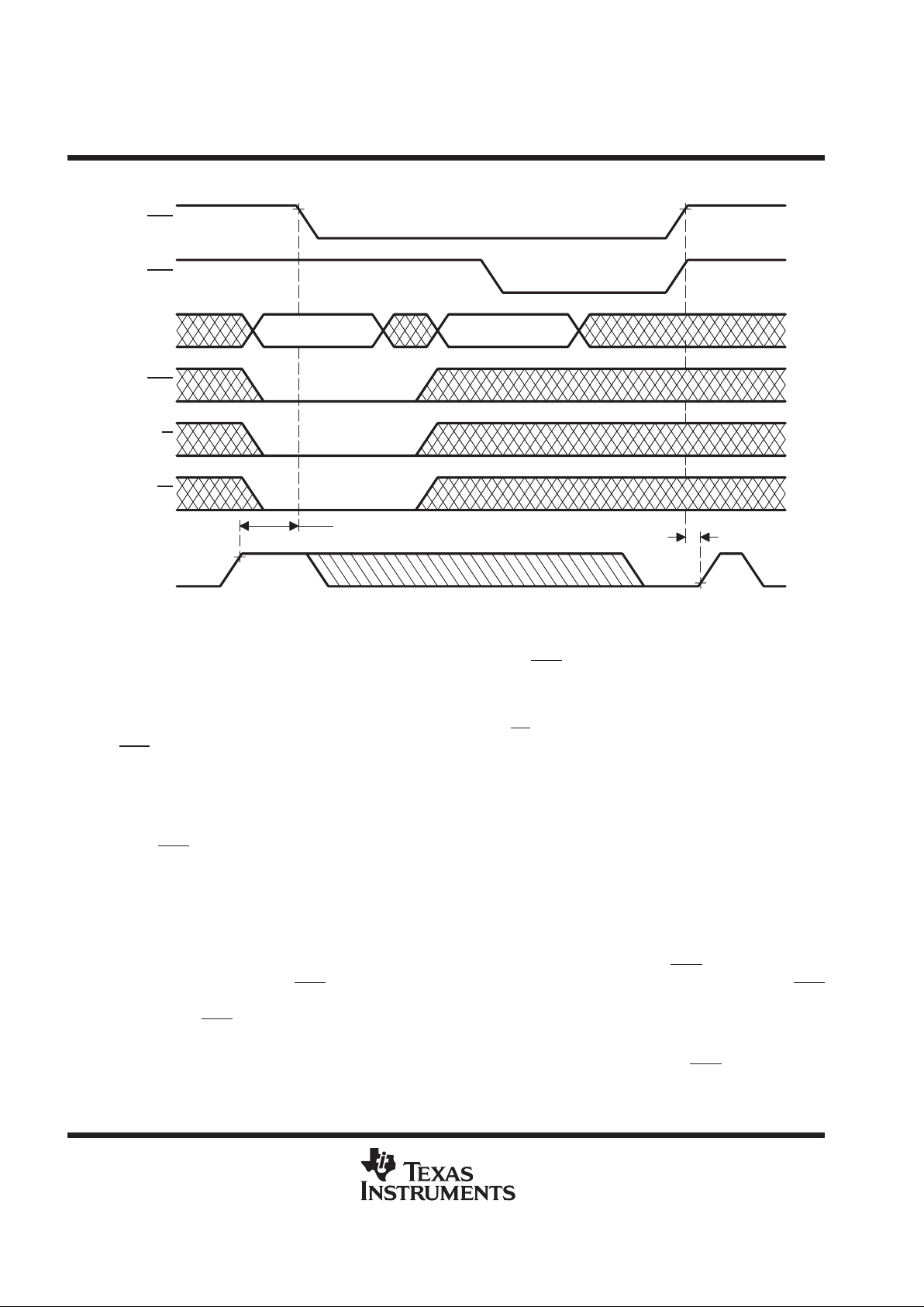
PARAMETER MEASUREMENT INFORMATION
Output
Pin
1.31 V
218 Ω
C
L
V
SS
Figure 12. Load Circuit
Page 25

SMJ44C251B
262144 BY 4-BIT
MULTIPORT VIDEO RAM
SGMS058A – MARCH 1995 – REVISED JUNE 1995
25
POST OFFICE BOX 1443 • HOUSTON, TEXAS 77251–1443
PARAMETER MEASUREMENT INFORMATION
RAS
CAS
A0–A8
DSF
TRG
W
DQ0–DQ3
t
c(rd)
t
w(RL)
t
d(RLCH)
t
w(RH)
t
d(CHRL)
t
d(CLRH)
t
w(CL)
t
d(RLCL)
t
t
t
h(RA)
t
d(CLGH)
t
w(CH)
t
h(CLCA)
t
su(RA)
t
su(TRG)
t
h(RHrd)
t
su(rd)
t
dis(G)
t
a(G)
t
a(C)
t
a(CA)
t
a(R)
Row Column
Valid Output
t
w(TRG)
t
h(TRG)
t
su(CA)
t
dis(CH)
t
d(GLRH)
t
d(DGL)
Data
In
Don’t Care
t
h(RLCA)
t
h(CHrd)
Figure 13. Read-Cycle Timing
Page 26

SMJ44C251B
262144 BY 4-BIT
MULTIPORT VIDEO RAM
SGMS058A – MARCH 1995 – REVISED JUNE 1995
26
POST OFFICE BOX 1443 • HOUSTON, TEXAS 77251–1443
PARAMETER MEASUREMENT INFORMATION
A0–A8
Row
RAS
CAS
DSF
TRG
W
DQ0–DQ3
t
su(RA)
t
t
Column
1
2
3
45
t
su(DQR)
t
c(W)
t
w(RL)
t
w(RH)
t
t
t
d(RLCH)
t
h(CLCA)
t
h(RA)
t
d(RLCL)
t
w(CL)
t
h(SFC)
t
su(SFC)
t
h(SFR)
t
su(SFR)
t
su(TRG)
t
h(TRG)
t
su(WMR)
t
su(WCH)
t
su(WRH)
t
h(RLW)
t
h(CLW)
t
su(WCL)
t
h(RWM)
t
w(WL)
t
h(CLD)
t
h(RLD)
t
h(RDQ)
t
su(DCL)
t
su(CA)
t
d(CLRH)
t
d(CHRL)
t
w(CH)
t
h(RLCA)
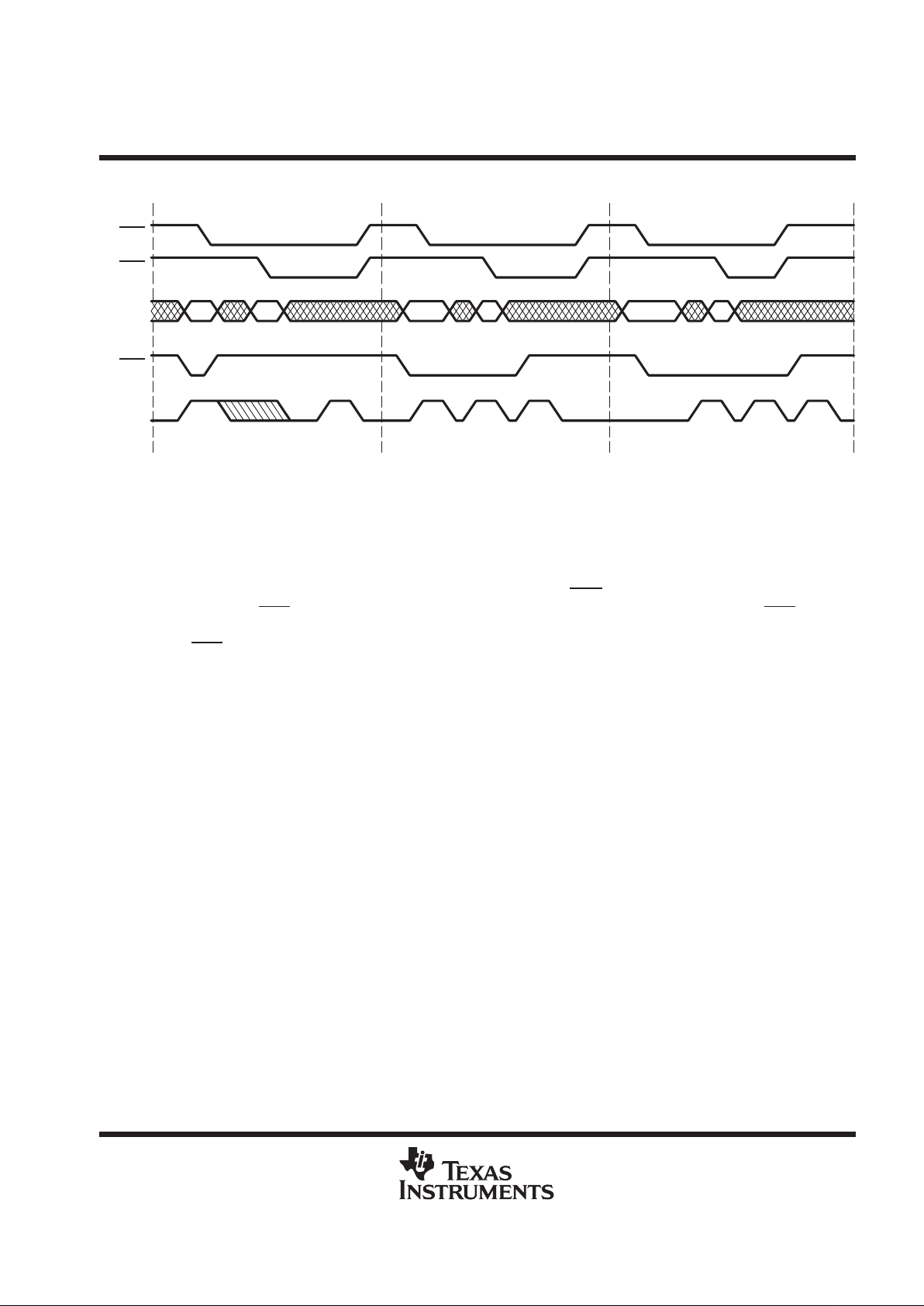
Figure 14. Early-Write-Cycle Timing
Table 4. Write-Cycle State Table
STATE
CYCLE
1 2 3 4 5
Write operation L L H Don’t care V alid data
Write-mask load/use, write DQs to I/Os L L L Write mask Valid data
Use previous write mask, write DQs to I/Os H L L Don’t care Valid data
Load write mask on later of W fall and CAS fall H L H Don’t care Write mask
Page 27

SMJ44C251B
262144 BY 4-BIT
MULTIPORT VIDEO RAM
SGMS058A – MARCH 1995 – REVISED JUNE 1995
27
POST OFFICE BOX 1443 • HOUSTON, TEXAS 77251–1443
PARAMETER MEASUREMENT INFORMATION
t
su(TRG)
RAS
CAS
DSF
TRG
W
DQ0–DQ3
t
c(W)
RowA0–A8 Column
12
3
45
t
w(RL)
t
d(RLCH)
t
d(CLRH)
t
w(RH)
t
t
t
d(CHRL)
t
w(CH)
t
w(CL)
t
d(RLCL)
t
t
t
h(RA)
t
h(RLCA)
t
su(CA)
t
su(RA)
t
h(CLCA)
t
h(SFC)
t
su(SFC)
t
su(SFR)
t
su(WRH)
t
su(WCH)
t
h(RLW)
t
d(GHD)
t
su(DWL)
t
w(WL)
t
h(WLD)
t
h(RLD)
t
h(RDQ)
t
h(SFR)
t
su(DQR)
t
h(RWM)
t
su(WMR)
t
d(CHRL)
t
d(RLCA)
t
d(CARH)
t
h(RSF)
t
h(WLG)
t
h(CLW)
Figure 15. Delayed-Write-Cycle Timing (Output-Enable-Controlled Write)
Table 5. Write-Cycle State Table
STATE
CYCLE
1 2 3 4 5
Write operation L L H Don’t care V alid data
Write-mask load/use, write DQs to I/Os L L L Write mask Valid data
Use previous write mask, write DQs to I/Os H L L Don’t care Valid data
Load write mask on later of W fall and CAS fall H L H Don’t care Write mask
Page 28

SMJ44C251B
262144 BY 4-BIT
MULTIPORT VIDEO RAM
SGMS058A – MARCH 1995 – REVISED JUNE 1995
28
POST OFFICE BOX 1443 • HOUSTON, TEXAS 77251–1443
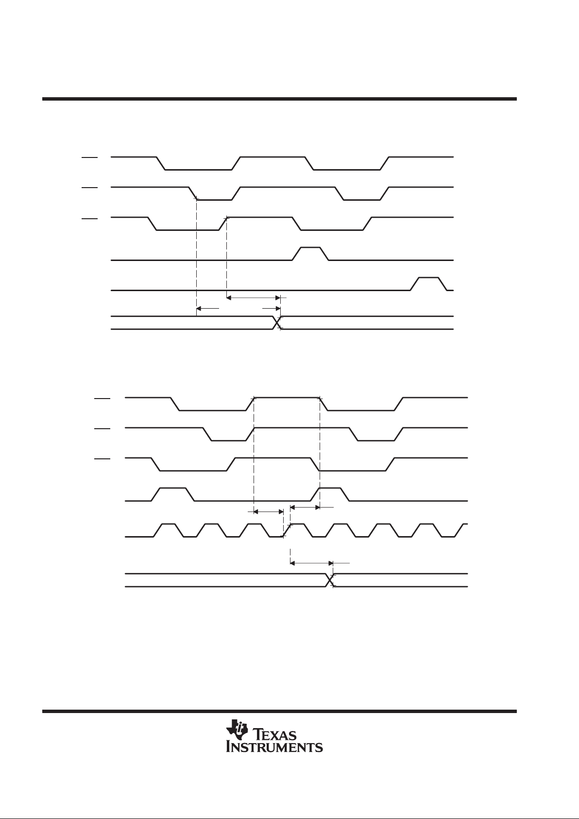
PARAMETER MEASUREMENT INFORMATION
RAS
CAS
DSF
TRG
W
0–
3
t
c(rdW)
A0–A8
t
w(RL)
t
d(CLRH)
t
w(RH)
t
d(CHRL)
t
w(CH)
t
h(CLCA)
t
su(CA)
t
h(RA)
t
su(RA)
t
h(RLCA)
t
h(SFR)
t
su(SFR)
t
h(SFC)
t
su(WCH)
t
su(WRH)
t
d(CAWL)
t
h(WLG)
t
su(rd)
t
w(TRG)
t
h(CLW)
t
w(WL)
t
h(WLD)
t
d(GHD)
t
su(DWL)
t
a(CA)
t
a(R)
t
a(C)
t
h(RDQ)
t
su(DQR)
t
a
(G)
t
dis(G)
t
h(RWM)
t
su(TRG)
t
su(WMR)
t
w(CL)
t
d(RLCL)
Row Column
Don’t Care
12
Don’t Care
3
4
Valid
Output
5
t
su(SFC)
t
d(RLCH)
t
d(CHRL)
t
d(RLCA)
t
d(CARH)
t
h(RSF)
t
h(TRG)
t
h(RLW)
t
d(DCL)
t
d(CLGH)
t
d(DGL)
t
d(RLWL)
t
d(CLWL)
Figure 16. Read-Write/Read-Modify-Write-Cycle Timing
Table 6. Write-Cycle State Table
STATE
CYCLE
1 2 3 4 5
Write operation L L H Don’t care V alid data
Write-mask load/use, write DQs to I/Os L L L Write mask Valid data
Use previous write mask, write DQs to I/Os H L L Don’t care Valid data
Load write mask on later of W fall and CAS fall H L H Don’t care Write mask
Page 29

SMJ44C251B
262144 BY 4-BIT
MULTIPORT VIDEO RAM
SGMS058A – MARCH 1995 – REVISED JUNE 1995
29
POST OFFICE BOX 1443 • HOUSTON, TEXAS 77251–1443
PARAMETER MEASUREMENT INFORMATION
t
w(RL)P
RAS
CAS
DSF
TRG
W
DQ0–
DQ3
A0–A8
t
d(RLCL)
t
w(CL)
t
w(CH)
t
d(CLRH)
t
w(RH)
t
d(CHRL)
t
a(CP)
t
d(CARH)
t
d(RLCH)
t
h(RA)
t
h(RLCA)
t
su(RA)
t
su(TRG)
t
h(RHrd)
t
h(CHrd)
t
su(rd)
t
su(WMR)
t
a(C)
t
a(CA)
t
a(G)
t
a(R)
‡
t
a(CP)
†
t
a(CA)
†
t
dis(G)
t
dis(CH)
‡
Valid Output
Row Column Column
t
h(CLCA)
t
h(TRG)
Don’t Care
t
d(CHRL)
Valid
Output
Data In
t
w(TRG)
t
d(GLRH)
t
w(TRG)
t
d(CLGH)
t
dis(G)
t
a(G)
t
dis(CH)
t
d(DGL)
t
d(DCL)
t
c(rdWP)
t
d(RLCA)
t
su(CA)
t
d(CLGH)
†
Access time is t
a(CP)
or t
a(CA)
dependent.
‡
Output can go from the high-impedance state to an invalid data state prior to the specified access time.
NOTE A: A write cycle or a read-modify-write cycle can be mixed with the read cycles as long as the write and read-modify-write timing
specifications are not violated and the proper polarity of DSF is selected on the falling edges of RAS
and CAS to select the desired write
mode (normal, block write, etc.)
Figure 17. Enhanced-Page-Mode Read-Cycle Timing
Page 30

SMJ44C251B
262144 BY 4-BIT
MULTIPORT VIDEO RAM
SGMS058A – MARCH 1995 – REVISED JUNE 1995
30
POST OFFICE BOX 1443 • HOUSTON, TEXAS 77251–1443
PARAMETER MEASUREMENT INFORMATION
t
w(RL)P
t
w(RH)
t
c(P)
t
w(CH)
t
d(CLRH)
t
d(RLCH)
t
d(RLCL)
t
h(RA)
t
su(RA)
t
su(CA)
t
h(CLCA)
t
h(RLCA)
t
su(SFC)
t
h(SFR)
t
su(SFR)
t
su(TRG)
t
su(WCH)
t
w(WL)
t
su(WRH)
t
su(WCH)
t
su(RWM)
t
su(WMR)
t
h(CLD)
†
t
su(DWL)
†
t
su(DCL)
†
t
h(RDQ)
t
h(RLD)
t
h(WLD)
†
t
su(DQR)
RAS
CAS
DSF
TRG
W
DQ0–DQ3
A0–A8
t
w(CL)
Row Column
12 2
3
Column
t
h(SFC)
t
d(CHRL)
t
d(CARH)
t
h(SFC)
t
su(SFC)
t
d(CHRL)
45 5
See Note A
t
h(TRG)
t
h(RSF)
t
d(RLCA)
†
Referenced to CAS or W, whichever occurs last
NOTE B: A read cycle or a read-modify-write cycle can be intermixed with write cycles, observing read and read-modify-write timing
specifications. TRG
must remain high throughout the entire page-mode operation to assure page-mode cycle time if the late-write
feature is used. If the early-write-cycle timing is used, the state of TRG
is a don’t care after the minimum period t
h(TRG)
from the falling
edge of RAS
.
Figure 18. Enhanced-Page-Mode Write-Cycle Timing
Table 7. Write-Cycle State Table
STATE
CYCLE
1 2 3 4 5
Write operation L L H Don’t care V alid data
Write-mask load/use, write DQs to I/Os L L L Write mask Valid data
Use previous write mask, write DQs to I/Os H L L Don’t care Valid data
Load write mask on later of W fall and CAS fall H L H Don’t care Write mask
Page 31

SMJ44C251B
262144 BY 4-BIT
MULTIPORT VIDEO RAM
SGMS058A – MARCH 1995 – REVISED JUNE 1995
31
POST OFFICE BOX 1443 • HOUSTON, TEXAS 77251–1443
PARAMETER MEASUREMENT INFORMATION
5
Valid
Out
RAS
CAS
W
DQ0–DQ3
TRG
A0–A8 Row Column
12 2
Column
3
45
Valid
Out
t
w(RL)P
t
d(RLCH)
t
c(rdWP)
t
w(CL)
t
d(RLCL)
t
w(CH)
t
d(CLRH)
t
d(CHRL)
t
w(RH)
t
su(RA)
t
su(SFR)
t
h(SFR)
t
su(SFC)
t
h(SFC)
t
su(SFC)
t
h(SFC)
t
d(DCL)
t
su(WRH)
t
w(WL)
t
d(CLWL)
t
d(CAWL)
t
d(RLWL)
t
su(rd)
t
su(WMR)
t
a(C)
†
t
a(CA)
†
t
su(DWL)
t
su(DQR)
t
h(TRG)
t
a(G)
†
t
a(R)
t
d(GHD)
t
dis(G)
DSF
t
su(CA)
t
h(RLCA)
t
h(RA)
t
d(CHRL)
t
d(RLCA)
t
h(CLCA)
t
d(CARH)
t
d(CLGH)
t
su(TRG)
t
h(RDQ)
t
d(CLGH)
t
su(WCH)
t
w(TPG)
t
h(RWM)
t
d(DCL)
t
w(TRG)
t
h(WLD)
t
su(DWL)
t
d(GHD)
t
h(WLD)
t
a(CP)
†
t
a(C)
†
t
d(DGL)
t
d(DGL)
†
Output can go from the high-impedance state to an invalid data state prior to the specified access time.
NOTE A: A read or a write cycle can be intermixed with read-modify-write cycles as long as the read and write timing specifications are not violated.
Figure 19. Enhanced-Page-Mode Read-Modify-Write-Cycle Timing
Table 8. Write-Cycle State Table
STATE
CYCLE
1 2 3 4 5
Write operation L L H Don’t care V alid data
Write-mask load/use, write DQs to I/Os L L L Write mask Valid data
Use previous write mask, write DQs to I/Os H L L Don’t care Valid data
Load write mask on later of W fall and CAS fall H L H Don’t care Write mask
Page 32

SMJ44C251B
262144 BY 4-BIT
MULTIPORT VIDEO RAM
SGMS058A – MARCH 1995 – REVISED JUNE 1995
32
POST OFFICE BOX 1443 • HOUSTON, TEXAS 77251–1443
PARAMETER MEASUREMENT INFORMATION
Valid Color Data Input
Refresh
Row
t
c(W)
t
w(RL)
t
w(RH)
t
t
t
t
t
d(RLCH)
RAS
CAS
A0–A8
DSF
TRG
W
DQ0–DQ3
t
d(CLRH)
t
d(CHRL)
t
w(CL)
t
d(RLCL)
t
d(CHRL)
t
w(CH)
t
h(RSF)
t
h(RA)
t
su(RA)
t
su(SFR)
t
su(SFC)
t
h(SFR)
t
h(SFC)
t
h(RSF)
t
su(TRG)
t
h(TRG)
t
su(WCH)
t
su(WRH)
t
h(RWM)
t
h(RLW)
t
su(WMR)
t
su(WCL)
t
h(CLW)
t
w(WL)
t
su(DCL)
t
h(CLD)
t
h(RLD)
Don’t Care
Figure 20. Load-Color-Register-Cycle Timing (Early-Write Load)
Page 33

SMJ44C251B
262144 BY 4-BIT
MULTIPORT VIDEO RAM
SGMS058A – MARCH 1995 – REVISED JUNE 1995
33
POST OFFICE BOX 1443 • HOUSTON, TEXAS 77251–1443
PARAMETER MEASUREMENT INFORMATION
RAS
CAS
A0–A8
DSF
TRG
W
DQ0–DQ3
t
c(W)
t
w(RL)
t
d(RLCH)
t
w(RH)
t
t
t
d(CLRH)
t
w(CL)
t
d(RLCL)
t
t
t
d(CHRL)
t
h(RSF)
t
h(RA)
t
su(RA)
t
w(CH)
Refresh
Row
t
h(SFC)
t
su(SFC)
t
su(SFR)
t
h(SFR)
t
su(WCH)
t
su(WRH)
t
su(TRG)
t
su(WMR)
t
d(GHD)
t
h(RWL)
t
h(CLW)
t
h(WLG)
t
w(WL)
t
su(DWL)
t
h(WLD)
t
h(RLD)
Valid Color Data Input
t
d(CHRL)
Don’t Care
Figure 21. Load-Color-Register-Cycle Timing (Delayed-Write Load)
Page 34

SMJ44C251B
262144 BY 4-BIT
MULTIPORT VIDEO RAM
SGMS058A – MARCH 1995 – REVISED JUNE 1995
34
POST OFFICE BOX 1443 • HOUSTON, TEXAS 77251–1443
PARAMETER MEASUREMENT INFORMATION
Block Address
A2–A8
t
c(W)
t
w(RL)
t
w(RH)
t
d(RLCH)
t
d(CHRL)
RAS
CAS
A0–A8
DSF
TRG
W
DQ0–DQ3
t
d(CLRH)
t
d(RLCL)
t
t
t
d(CHRL)
t
w(CL)
t
h(RLCA)
t
d(CARH)
t
w(CH)
t
h(CLCA)
t
d(RLCA)
t
su(RA)
t
h(RA)
t
su(CA)
t
h(RSF)
t
h(SFC)
t
su(SFC)
t
su(SFR)
t
h(SFR)
Row
1
2
34
t
su(TRG)
t
h(RWM)
t
h(TRG)
t
su(WMR)
t
su(WCH)
t
su(WRH)
t
h(CLW)
t
h(RLW)
t
w(WL)
t
su(DCL)
t
h(RLD)
t
h(CLD)
t
h(RDQ)
t
su(DQR)
t
t
t
su(WCL)
Figure 22. Block-Write-Cycle Timing (Early Write)
Table 9. Block-Write-Cycle State Table
STATE
CYCLE
1 2 3 4
Write-mask load/use, block write L L Write mask Column mask
Use previous write mask, block write H L Don’t care Column mask
Write mask disabled, block write to all I/Os L H Don’t care Column mask
Write mask data 0: I/O write disable
1: I/O write enable
Column mask data DQn = 0 column write disable
(n = 0, 1, 2, 3) 1 column write enable
DQ0 — column 0 (address A1 = 0, A0 = 0)
DQ1 — column 1 (address A1 = 0, A0 = 1)
DQ2 — column 2 (address A1 = 1, A0 = 0)
DQ3 — column 3 (address A1 = 1, A0 = 1)
Page 35

SMJ44C251B
262144 BY 4-BIT
MULTIPORT VIDEO RAM
SGMS058A – MARCH 1995 – REVISED JUNE 1995
35
POST OFFICE BOX 1443 • HOUSTON, TEXAS 77251–1443
PARAMETER MEASUREMENT INFORMATION
t
c(W)
t
w(RL)
t
w(RH)
t
d(RLCH)
t
t
t
t
t
d(RLCL)
t
d(CLRH)
t
w(CL)
t
d(CHRL)
t
w(CH)
t
h(RA)
t
su(RA)
t
su(CA)
2
34
t
su(TRG)
t
h(RWM)
t
d(GHD)
t
su(WRH)
t
su(WCH)
t
h(RLW)
t
h(CLW)
t
su(WMR)
t
su(DQR)
t
h(RDQ)
t
su(DWL)
t
w(WL)
t
h(WLD)
t
h(RLD)
RAS
CAS
A0–A8
W
TRG
DQ0–DQ3
DSF
Row
t
su(SFR)
t
h(SFR)
t
h(SFC)
t
su(SFC)
t
d(CHRL)
t
d(RLCA)
t
d(CARH)
t
h(WLG)
t
h(RSF)
t
h(RLCA)
Block Address
A2–A8
t
h(CLCA)
1
Figure 23. Block-Write-Cycle Timing (Delayed-Write)
Table 10. Block-Write-Cycle State Table
STATE
CYCLE
1 2 3 4
Write-mask load/use, block write L L Write mask Column mask
Use previous write mask, block write H L Don’t care Column mask
Write mask disabled, block write to all I/Os L H Don’t care Column mask
Write mask data 0: I/O write disable
1: I/O write enable
Column mask data DQn = 0 column write disable
(n = 0, 1, 2, 3) 1 column write enable
DQ0 — column 0 (address A1 = 0, A0 = 0)
DQ1 — column 1 (address A1 = 0, A0 = 1)
DQ2 — column 2 (address A1 = 1, A0 = 0)
DQ3 — column 3 (address A1 = 1, A0 = 1)
Page 36

SMJ44C251B
262144 BY 4-BIT
MULTIPORT VIDEO RAM
SGMS058A – MARCH 1995 – REVISED JUNE 1995
36
POST OFFICE BOX 1443 • HOUSTON, TEXAS 77251–1443
PARAMETER MEASUREMENT INFORMATION
RAS
CAS
A0–A8
W
TRG
DSF
DQ0–DQ3
t
w(RL)P
t
d(RLCH)
t
d(RLCL)
t
w(CL)
t
w(CH)
t
c(P)
t
d(CLRH)
t
d(CHRL)
t
w(RH)
t
su(RA)
t
h(RA)
t
su(CA)
t
h(CLCA)
t
d(CARH)
2
t
su(WMR)
t
h(RWM)
t
su(SFR)
t
h(SFR)
t
h(SFC)
t
su(SFC)
t
h(SFC)
t
su(WCH)
t
w(WL)
t
su(WCH)
t
su(WRH)
t
su(DQR)
t
h(RDQ)
t
su(DWL)
†
t
su(DCL)
†
t
h(CLD)
†
t
h(WLD)
†
t
h(RLD)
Row
Block Address
A2–A8
34 4
Block Address
A2–A8
t
h(TRG)
See Note A
t
d(RLCA)
t
d(CHRL)
t
h(RLCA)
t
su(TRG)
t
su(SFC)
1
†
Referenced to CAS or W, whichever occurs last
NOTE A: TRG
must remain high throughout the entire page-mode operation to assure page-mode cycle time if the late write feature is used. If
the early-write-cycle timing is used, the state of TRG
is a don’t care after the minimum period t
h(TRG)
from the falling edge of RAS.
Figure 24. Enhanced-Page-Mode Block-Write-Cycle Timing
Table 11. Enhanced-Page-Mode Block-Write-Cycle Table
STATE
CYCLE
1 2 3 4
Write-mask load/use, block write L L Write mask Column mask
Use previous write mask, block write H L Don’t care Column mask
Write mask disabled, block write to all I/Os L H Don’t care Column mask
Write mask data 0: I/O write disable
1: I/O write enable
Column mask data DQn = 0 column write disable
(n = 0, 1, 2, 3) 1 column write enable
DQ0 — column 0 (address A1 = 0, A0 = 0)
DQ1 — column 1 (address A1 = 0, A0 = 1)
DQ2 — column 2 (address A1 = 1, A0 = 0)
DQ3 — column 3 (address A1 = 1, A0 = 1)
Page 37

SMJ44C251B
262144 BY 4-BIT
MULTIPORT VIDEO RAM
SGMS058A – MARCH 1995 – REVISED JUNE 1995
37
POST OFFICE BOX 1443 • HOUSTON, TEXAS 77251–1443
PARAMETER MEASUREMENT INFORMATION
RAS
CAS
DSF
TRG
W
DQ0–DQ3
A0–A8
t
c(rd)
t
w(RL)
t
w(RH)
t
t
t
h(RA)
t
su(RA)
t
su(SFR)
t
su(TRG)
t
h(TRG)
t
h(SFR)
t
t
Row Row
t
d(CHRL)
t
d(RHCL)
t
d(CHRL)
Don’t Care
Don’t Care
Don’t Care
Don’t Care
Don’t Care
Don’t Care
NOTE A: In persistent write-per-bit function, W
must be high at the falling edge of RAS during the refresh cycle.
Figure 25. RAS-Only Refresh-Cycle Timing
Page 38

SMJ44C251B
262144 BY 4-BIT
MULTIPORT VIDEO RAM
SGMS058A – MARCH 1995 – REVISED JUNE 1995
38
POST OFFICE BOX 1443 • HOUSTON, TEXAS 77251–1443
PARAMETER MEASUREMENT INFORMATION
RAS
t
c(rd)
t
w(RL)
t
w(RH)
t
d(RHCL)RF
t
d(CLRL)RF
t
d(RLCH)RF
CAS
A0–A8
DSF
TRG
W
DQ0–DQ3
Don’t Care
t
dis(CH)
Valid Out
Hi-Z
t
d(CHRL)
Don’t Care
Don’t Care
Don’t Care
NOTE A: In persistent write-per-bit operation, W must be high at the falling edge of RAS during the refresh cycle.
Figure 26. CBR-Refresh-Cycle Timing
Page 39

SMJ44C251B
262144 BY 4-BIT
MULTIPORT VIDEO RAM
SGMS058A – MARCH 1995 – REVISED JUNE 1995
39
POST OFFICE BOX 1443 • HOUSTON, TEXAS 77251–1443
PARAMETER MEASUREMENT INFORMATION
t
su(CA)
RAS
CAS
A0–A8
W
TRG
DSF
DQ0–DQ3
t
w(RL)
t
w(RH)
t
w(RH)
t
w(RL)
t
w(CL)
t
d(RLCH)
t
h(CLCA)
t
h(RA)
t
h(RHrd)
Don’t CareRow Col
Don’t Care
t
dis(CH)
t
a(C)
t
a(R)
Valid Data
t
su(RA)
t
c(rd)
t
c(rd)
t
c(rd)
t
d(RLCA)
t
d(CHRL)
t
d(CARH)
t
d(GLRH)
t
a(G)
t
dis(G)
Don’t Care
Memory Read Cycle
Refresh Cycle
Refresh Cycle
t
su(RD)
t
h(TRG)
t
su(TRG)
Figure 27. Hidden-Refresh-Cycle Timing
Page 40

SMJ44C251B
262144 BY 4-BIT
MULTIPORT VIDEO RAM
SGMS058A – MARCH 1995 – REVISED JUNE 1995
40
POST OFFICE BOX 1443 • HOUSTON, TEXAS 77251–1443
PARAMETER MEASUREMENT INFORMATION
RAS
CAS
A0–A8
W
TRG
DSF
SC
SDQ0–SDQ3
SE
t
c(TW)
t
w(RL)
t
d(RLCL)
t
d(RLCH)
t
w(CL)
t
h(RA)
t
h(CLCA)
Row
Tap Point
A0–A8
Don’t Care
t
h(SFR)
Don’t Care
Don’t Care
Don’t Care
t
su(TRG)
t
h(TRG)
t
su(WMR)
t
h(RWM)
t
d(RHSC)
t
w(SCH)
t
w(SCL)
t
h(SDS)
t
su(SDS)
Valid Data
Input
t
dis(SE)
t
su(SE)
t
h(SE)
t
d(SESC)
DQ0–DQ3
Hi-Z
QSF
Tap Point
Bit A7
t
w(RH)
t
d(CARH)
t
d(CHRL)
t
w(CH)
t
su(CA)
t
d(RLCA)
t
w(SCH)
t
d(RLSD)
Valid Data Output
t
h(RLSQ)
t
d(CLQSF)
t
d(GHQSF)
t
d(RLQSF)
t
su(RA)
t
h(RLCA)
t
su(SFR)
t
d(SCRL)
NOTE: The write-mode-control cycle is used to change the SDQs from the output mode to the input mode. This allows serial data to be written
into the data register. This figure assumes that the device was originally in the serial-read mode.
Figure 28. Write-Mode-Control Pseudo-Transfer Timing
Page 41

SMJ44C251B
262144 BY 4-BIT
MULTIPORT VIDEO RAM
SGMS058A – MARCH 1995 – REVISED JUNE 1995
41
POST OFFICE BOX 1443 • HOUSTON, TEXAS 77251–1443
PARAMETER MEASUREMENT INFORMATION
RAS
CAS
A0–A8
W
TRG
DSF
SC
SDQ0–SDQ3
SE
t
c(TW)
t
w(RL)
t
d(RLCL)
t
d(RLCH)
t
w(CL)
t
h(RA)
t
h(CLCA)
Row
Tap Point
A0–A8
Don’t Care
t
su(TRG)
t
h(TRG)
t
su(WMR)
t
h(RWM)
t
d(RHSC)
t
w(SCH)
t
w(SCL)
t
h(SDS)
t
su(SDS)
Data In
t
su(SE)
t
d(SESC)
DQ0–DQ3
Hi-Z
QSF
Tap Point
Bit A7
t
w(RH)
t
d(CARH)
t
d(CHRL)
t
w(CH)
t
su(CA)
t
d(RLCA)
t
w(SCH)
Data In
t
su(SDS)
t
d(CLQSF)
t
d(GHQSF)
t
d(RLQSF)
t
su(RA)
t
h(RLCA)
t
d(SCRL)
t
d(CARH)
Don’t Care
Don’t Care
t
h(SE)
t
h(SDS)
Don’t Care
Figure 29. Data-Register-to-Memory Transfer Timing, Serial Input Enabled
Page 42

SMJ44C251B
262144 BY 4-BIT
MULTIPORT VIDEO RAM
SGMS058A – MARCH 1995 – REVISED JUNE 1995
42
POST OFFICE BOX 1443 • HOUSTON, TEXAS 77251–1443
PARAMETER MEASUREMENT INFORMATION
RAS
CAS
A0–A8
W
TRG
DSF
SC
SDQ0–SDQ3
SE
t
c(TW)
t
w(RL)
t
d(RLCL)
t
d(RLCH)
t
w(CL)
t
h(RA)
t
h(CLCA)
Row
Tap Point
A0–A8
Don’t Care
t
su(TRG)
t
h(TRG)
t
su(WMR)
t
h(RWM)
t
d(RHSC)
t
w(SCH)
t
w(SCL)
t
h(SDS)
t
su(SDS)
Data In
t
d(SESC)
DQ0–DQ3
Hi-Z
QSF
Tap Point
Bit A7
t
w(RH)
t
d(CARH)
t
d(CHRL)
t
w(CH)
t
su(CA)
t
d(RLCA)
t
w(SCH)
Data In
t
su(SDS)
t
d(CLQSF)
t
d(GHQSF)
t
d(RLQSF)
t
su(RA)
t
h(RLCA)
t
d(SCRL)
Don’t Care
t
h(SDS)
t
su(SRF)
t
h(SFR)
Don’t Care
Don’t Care
t
d(SCSE)
Don’t Care
Figure 30. Alternate Data-Register-to-Memory Transfer-Cycle Timing
Page 43

SMJ44C251B
262144 BY 4-BIT
MULTIPORT VIDEO RAM
SGMS058A – MARCH 1995 – REVISED JUNE 1995
43
POST OFFICE BOX 1443 • HOUSTON, TEXAS 77251–1443
PARAMETER MEASUREMENT INFORMATION
RAS
CAS
DSF
TRG
W
SC
A0–A8
SE
Row
Tap Point
A0–A8
Don’t Care
SDQ0–SDQ3
H
L
Don’t Care
Old Data Old Data New Data
t
c(TRD)
t
d(RLCL)
t
w(RL)
t
d(RLCH)
t
w(CL)
t
h(RLCA)
t
su(RA)
t
h(RA)
t
su(CA)
t
h(CLCA)
t
su(SFR)
t
su(TRG)
t
su(WMR)
t
h(RWM)
t
d(CLSH)
t
d(RLSH)
t
w(SCH)
t
a(SQ)
t
h(SHSQ)
t
c(SC)
t
a(SQ)
t
h(SHSQ)
t
w(RH)
t
h(TRG)
DQ0–DQ3
Hi-Z
QSF
Tap Point bit A7
t
d(CHRL)
t
d(RLCA)
t
d(CARH)
t
w(GH)
t
d(CASH)
t
d(SCTR)
t
w(SCL)
t
w(SCH)
t
d(GHQSF)
t
d(RLQSF)
t
d(CLQSF)
t
h(SFR)
NOTES: A. Early-load operation is defined as t
h(TRG)
min < t
h(TRG)
< t
d(RLTH)
min.
B. DQ outputs remain in the high-impedance state for the entire memory-to-data-register transfer cycle. The memory-to-data-register
transfer cycle is used to load the data registers in parallel from the memory array. The 512 locations in each data register are written
from the 512 corresponding columns of the selected row. The data that is transferred into the data registers can be either shifted
out or transferred back into another row.
C. Once data is transferred into the data registers, the SAM is in the serial-read mode (i.e., SQ is enabled), allowing data to be shifted
out of the registers. Also, the first bit to be read from the data register after TRG
has gone high must be activated by a positive
transition of SC.
Figure 31. Memory-to-Data-Register Transfer-Cycle Timing, Early-Load Operation
Page 44

SMJ44C251B
262144 BY 4-BIT
MULTIPORT VIDEO RAM
SGMS058A – MARCH 1995 – REVISED JUNE 1995
44
POST OFFICE BOX 1443 • HOUSTON, TEXAS 77251–1443
PARAMETER MEASUREMENT INFORMATION
RAS
CAS
DSF
TRG
W
SC
A0–A8
SE
Row
Don’t Care
SDQ0–SDQ3
H
L
Don’t Care
Old Data Old Data Old Data New Data
t
c(TRD)
t
d(RLCL)
t
w(RL)
t
d(RLCH)
t
w(CL)
t
h(RLCA)
t
su(RA)
t
h(RA)
t
su(CA)
t
h(CLCA)
t
su(SFR)
t
su(TRG)
t
su(WMR)
t
h(RWM)
t
d(THRH)
t
d(THRL)
t
d(THSC)
t
w(SCH)
t
a(SQ)
t
h(SHSQ)
t
c(SC)
t
a(SQ)
t
h(SHSQ)
t
w(RH)
t
d(RLTH)
t
w(SCL)
t
d(SCTR)
QSF Tap Point Bit A7
t
d(GHQSF)
t
d(RLQSF)
t
d(CLQSF)
DQ0–DQ3 Hi-Z
t
w(GH)
t
h(SFR)
t
d(CLGH)
t
d(CAGH)
Tap Point
A0–A8
t
d(RLCA)
Don’t Care
t
d(CHRL)
NOTES: A. Late-load operation is defined as t
d(THRH)
< 0 ns.
B. DQ outputs remain in the high-impedance state for the entire memory-to-data-register transfer cycle. The memory-to-data-register
transfer cycle is used to load the data registers in parallel from the memory array. The 512 locations in each data register are written
from the 512 corresponding columns of the selected row. The data that is transferred into the data registers can be either shifted
out or transferred back into another row.
C. Once data is transferred into the data registers, the SAM is in the serial read mode (i.e., SQ is enabled), allowing data to be shifted
out of the registers. Also, the first bit to be read from the data register after TRG
has gone high must be activated by a positive
transition of SC.
Figure 32. Memory-to-Data-Register Transfer-Cycle Timing,
Real-Time-Reload Operation/Late-Load Operation
Page 45

SMJ44C251B
262144 BY 4-BIT
MULTIPORT VIDEO RAM
SGMS058A – MARCH 1995 – REVISED JUNE 1995
45
POST OFFICE BOX 1443 • HOUSTON, TEXAS 77251–1443
PARAMETER MEASUREMENT INFORMATION
Tap Point
A0–A8
RAS
CAS
DSF
TRG
W
SC
A0–A8
SE
Row Don’t Care
SDQ0–SDQ3
H
L
Don’t Care
Valid In Invalid Out Valid Out
t
c(TRD)
t
d(RLCL)
t
w(RL)
t
d(RLCH)
t
w(CL)
t
h(RLCA)
t
su(RA)
t
h(RA)
t
su(CA)
t
h(CLCA)
t
su(SFR)
t
su(TRG)
t
su(WMR)
t
h(RWM)
t
d(CLSH)
t
d(RLSH)
t
d(SCRL)
t
su(SDS)
t
c(SC)
t
a(SQ)
t
w(RH)
t
h(TRG)
DQ0–DQ3
Hi-Z
QSF
Tap Point bit A7
t
d(CHRL)
t
d(RLCA)
t
d(CARH)
t
w(GH)
t
d(THSC)
t
d(GHQSF)
t
d(RLQSF)
t
d(CLQSF)
t
h(SFR)
t
d(CLGH)
t
d(THRL)
t
d(THRH)
t
d(RLTH)
t
h(SDS)
t
d(SDRL)
t
d(CAGH)
Don’t Care
Don’t Care
NOTES: A. Late-load operation is defined as t
d(THRH)
< 0 ns.
B. DQ outputs remain in the high-impedance state for the entire memory-to-data-register transfer cycle. The memory-to-data-register
transfer cycle is used to load the data registers in parallel from the memory array. The 512 locations in each data register are written
from the 512 corresponding columns of the selected row. The data that is transferred into the data registers may be either shifted
out or transferred back into another row.
C. Once data is transferred into the data registers, the SAM is in the serial read mode (i.e., SQ is enabled), allowing data to be shifted
out of the registers. Also, the first bit to be read from the data register after TRG
has gone high must be activated by a positive
transition of SC.
Figure 33. Memory-to-Data-Register Transfer-Cycle Timing, SDQ Ports Previously in Serial-Input Mode
Page 46

SMJ44C251B
262144 BY 4-BIT
MULTIPORT VIDEO RAM
SGMS058A – MARCH 1995 – REVISED JUNE 1995
46
POST OFFICE BOX 1443 • HOUSTON, TEXAS 77251–1443
PARAMETER MEASUREMENT INFORMATION
t
c(TRD)
t
w(RL)
t
d(RLCL)
t
d(RLCH)
t
w(CL)
t
h(RA)
t
su(CA)
t
h(CLCA)
t
su(TRG)
t
h(TRG)
t
h(SFR)
t
su(WMR)
t
h(RWM)
t
su(SFR)
Old MSB New MSB
Don’t Care
Don’t Care
Don’t CareRow Tap Point A0–A8
t
d(RHMS)
t
w(SCH)
t
a(SQ)
t
h(SHSQ)
Bit 255
or 511
Bit 255
or 511
Tap
Point N
Bit 254 or
Bit 510
H
L
RAS
CAS
A0–A8
W
TRG
DSF
SDQ0–SDQ3
QSF
SC
SE
Bit 255 or
Bit 511
Tap
Point N
t
c(SC)
t
w(CH)
t
d(CARH)
t
d(CHRL)
Tap
Point M
t
d(SCQSF)
t
d(MSRL)
t
c(SC)
t
w(SCL)
t
d(SCQSF)
t
a(SQ)
t
a(SQ)
t
a(SQ)
Tap Point M
Bit 255 or
Bit 511
t
d(RLCA)
t
w(SCL)
t
su(RA)
t
w(RH)
DQ0–DQ3
Hi-Z
t
d(THRH)
t
w(GH)
Figure 34. Split-Register-Mode Read-Transfer-Cycle Timing
Page 47

SMJ44C251B
262144 BY 4-BIT
MULTIPORT VIDEO RAM
SGMS058A – MARCH 1995 – REVISED JUNE 1995
47
POST OFFICE BOX 1443 • HOUSTON, TEXAS 77251–1443
PARAMETER MEASUREMENT INFORMATION
RAS
CAS
A0–A8
TRG
DSF
CASE I
SC
QSF
SC
QSF
SC
QSF
CASE II
CASE III
Tap1
(low)
Bit
255
Tap1
(high)
Bit
511
Tap2
(low)
Bit
255
Tap1
(low)
Row Tap1
(high)
Row Tap2
(low)
Row Tap2
(high)
Row
Tap1
(low)
Tap2
(low)
Bit
255
Bit
511
Bit
255
Tap1
(low)
Tap2
(low)
Bit
255
Bit
511
Bit
255
Tap1
(high)
Tap1
(high)
Normal Read Transfer
Split Register to the
High Half of the
Data Register
Split Register to the
Low Half of the
Data Register
Split Register to the
High Half of the
Data Register
NOTES: A. In order to achieve proper split-register operation, a normal read transfer should be performed before the first split-register transfer
cycle. This is necessary to initialize the data register and the starting tap location. First serial access can then begin either after the
normal read-transfer cycle (CASE I), during the first split-register cycle (CASE II), or even after the first split-register transfer cycle
(CASE III). There is no minimum requirement of SC clock between the normal read-transfer cycle and the first split-register cycle.
B. A split register transfer into the inactive half is not allowed until t
d(MSRL)
is met. t
d(MSRL)
is the minimum delay time between the rising
edge of the serial clock of the last bit (bit 255 or 511) and the falling edge of RAS
of the split-register transfer cycle into the inactive
half. After t
d(MSRL)
is met, the split-register transfer into the inactive half must also satisfy the t
d(RHMS)
requirement. t
d(RHMS)
is the
minimum delay time between the rising edge of RAS
of the split-register transfer cycle into the inactive half and the rising edge of
the serial clock of the last bit (bit 255 or 511). There is a minimum requirement of one rising edge of SC clock between two split-register
transfer cycles.
Figure 35. Split-Register-Transfer Operating Sequence
Page 48

SMJ44C251B
262144 BY 4-BIT
MULTIPORT VIDEO RAM
SGMS058A – MARCH 1995 – REVISED JUNE 1995
48
POST OFFICE BOX 1443 • HOUSTON, TEXAS 77251–1443
PARAMETER MEASUREMENT INFORMATION
t
w(SCH)
t
w(SCL)
t
w(SCH)
t
w(SCL)
t
w(SCH)
t
h(TRG)
t
su(TRG)
t
su(SDS)
t
h(SDS)
t
c(SC)
t
c(SC)
RAS
TRG
SC
SDQ0–SDQ3
Valid In
Valid In
t
su(SDS)
t
h(SDS)
Valid In
t
su(SDS)
t
h(SDS)
NOTES: A. The serial data-in cycle is used to input serial data into the data registers. Before data can be written into the data registers via the
SDQ terminals, the device must be put into the write mode by performing a write-mode-control (pseudo-transfer) cycle or any other
write-transfer cycle. A read-transfer cycle is the only cycle that takes the serial port (SAM) out of the write mode and puts it into the
read mode, disabling the input data. Data is written starting at the location specified by the input address loaded on the previous
transfer cycle.
B. While accessing data in the serial-data registers, the state of TRG
is a don’t care as long as TRG is held high when RAS goes low
to prevent data transfers between memory and data registers.
Figure 36. Serial-Write-Cycle Timing (SE = VIL)
Page 49

SMJ44C251B
262144 BY 4-BIT
MULTIPORT VIDEO RAM
SGMS058A – MARCH 1995 – REVISED JUNE 1995
49
POST OFFICE BOX 1443 • HOUSTON, TEXAS 77251–1443
PARAMETER MEASUREMENT INFORMATION
t
w(SCH)
t
w(SCL)
t
w(SCH)
t
w(SCL)
t
w(SCH)
t
h(TRG)
t
su(TRG)
t
su(SDS)
t
h(SDS)
t
c(SC)
t
c(SC)
RAS
TRG
SC
SDQ0–SDQ3
Valid In
Valid In
t
su(SDS)
t
h(SDS)
SE
t
d(SESC)
t
h(SCSE)
t
w(SEH)
t
su(SESC)
t
w(SEL)
t
d(SCSE)
t
d(SESC)
NOTES: A. The serial data-in cycle is used to input serial data into the data registers. Before data can be written into the data registers via the
SDQ terminals, the device must be put into the write mode by performing a write-mode-control (pseudo-transfer) cycle or any other
write-transfer cycle. A read-transfer cycle is the only cycle that takes the serial port (SAM) out of the write mode and puts it into the
read mode, disabling the input data. Data is written starting at the location specified by the input address loaded on the previous
transfer cycle.
B. While accessing data in the serial-data registers, the state of TRG
is a don’t care as long as TRG is held high when RAS goes low
to prevent data transfers between memory and data registers.
Figure 37. Serial-Write-Cycle Timing (SE-Controlled Write)
Page 50

SMJ44C251B
262144 BY 4-BIT
MULTIPORT VIDEO RAM
SGMS058A – MARCH 1995 – REVISED JUNE 1995
50
POST OFFICE BOX 1443 • HOUSTON, TEXAS 77251–1443
PARAMETER MEASUREMENT INFORMATION
t
w(SCH)
t
w(SCL)
t
w(SCH)
t
w(SCL)
t
w(SCH)
t
h(TRG)
t
su(TRG)
t
a(SQ)
t
h(SHSQ)
t
c(SC)
t
c(SC)
RAS
TRG
SC
SDQ0–SDQ3
Valid Out Valid Out Valid Out
t
a(SQ)
t
h(SHSQ)
t
a(SQ)
t
h(SHSQ)
Valid Out
NOTES: A. While reading data through the serial-data register , the state of TRG
is a don’t care as long as TRG is held high when RAS goes
low. This is to avoid the initiation of a register-to-memory-to-register data-transfer operation.
B. The serial data-out cycle is used to read data out of the data registers. Before data can be read via SDQ, the device must be put
into the read mode by performing a transfer-read cycle. Any transfer-write cycles occurring between the transfer-read cycle and the
subsequent shifting out of data take the device out of the read mode and put it in the write mode, not allowing the reading of data.
Figure 38. Serial-Read-Cycle Timing (SE = VIL)
Page 51

SMJ44C251B
262144 BY 4-BIT
MULTIPORT VIDEO RAM
SGMS058A – MARCH 1995 – REVISED JUNE 1995
51
POST OFFICE BOX 1443 • HOUSTON, TEXAS 77251–1443
PARAMETER MEASUREMENT INFORMATION
t
w(SCH)
t
w(SCL)
t
w(SCH)
t
w(SCL)
t
w(SCH)
t
h(TRG)
t
su(TRG)
t
a(SQ)
t
h(SHSQ)
t
c(SC)
t
c(SC)
RAS
TRG
SC
SDQ0–SDQ3
Valid Out Valid Out Valid Out
t
a(SQ)
t
dis(SE)
t
a(SQ)
t
h(SHSQ)
Valid Out
SE
Data
In
t
d(SDSE)
t
a(SE)
NOTES: A. While reading data through the serial-data register , the state of TRG is a don’t care as long as TRG is held high when RAS goes
low. This is to avoid the initiation of a register-to-memory-to-register data-transfer operation.
B. The serial data-out cycle is used to read data out of the data registers. Before data can be read via SDQ, the device must be put
into the read mode by performing a transfer-read cycle. Any transfer-write cycles occurring between the transfer-read cycle and the
subsequent shifting out of data take the device out of the read mode and put it in the write mode, not allowing the reading of data.
Figure 39. Serial-Read-Cycle Timing (SE-Controlled Read)
device symbolization
Speed (-10, -12)
Package Code
JD = ZIP
Lot Traceability Code
Date Code
Assembly Site Code
Die Revision Code
Wafer Fab Code
F R A XXX LLL
-SS
SMJ44C251B
TI
JD
Page 52

SMJ44C251B
262144 BY 4-BIT
MULTIPORT VIDEO RAM
SGMS058A – MARCH 1995 – REVISED JUNE 1995
52
POST OFFICE BOX 1443 • HOUSTON, TEXAS 77251–1443
Page 53

IMPORTANT NOTICE
T exas Instruments and its subsidiaries (TI) reserve the right to make changes to their products or to discontinue
any product or service without notice, and advise customers to obtain the latest version of relevant information
to verify, before placing orders, that information being relied on is current and complete. All products are sold
subject to the terms and conditions of sale supplied at the time of order acknowledgement, including those
pertaining to warranty, patent infringement, and limitation of liability.
TI warrants performance of its semiconductor products to the specifications applicable at the time of sale in
accordance with TI’s standard warranty. Testing and other quality control techniques are utilized to the extent
TI deems necessary to support this warranty. Specific testing of all parameters of each device is not necessarily
performed, except those mandated by government requirements.
CERT AIN APPLICATIONS USING SEMICONDUCTOR PRODUCTS MAY INVOLVE POTENTIAL RISKS OF
DEATH, PERSONAL INJURY, OR SEVERE PROPERTY OR ENVIRONMENTAL DAMAGE (“CRITICAL
APPLICATIONS”). TI SEMICONDUCTOR PRODUCTS ARE NOT DESIGNED, AUTHORIZED, OR
WARRANTED TO BE SUITABLE FOR USE IN LIFE-SUPPORT DEVICES OR SYSTEMS OR OTHER
CRITICAL APPLICATIONS. INCLUSION OF TI PRODUCTS IN SUCH APPLICA TIONS IS UNDERST OOD TO
BE FULLY AT THE CUSTOMER’S RISK.
In order to minimize risks associated with the customer’s applications, adequate design and operating
safeguards must be provided by the customer to minimize inherent or procedural hazards.
TI assumes no liability for applications assistance or customer product design. TI does not warrant or represent
that any license, either express or implied, is granted under any patent right, copyright, mask work right, or other
intellectual property right of TI covering or relating to any combination, machine, or process in which such
semiconductor products or services might be or are used. TI’s publication of information regarding any third
party’s products or services does not constitute TI’s approval, warranty or endorsement thereof.
Copyright 1998, Texas Instruments Incorporated
 Loading...