

Page 1
SMJ28F010B
131072 BY 8-BIT
FLASH MEMORY
SGMS738 – APRIL 1998
1
POST OFFICE BOX 1443 • HOUSTON, TEXAS 77251–1443
D
Organization . . . 131072 × 8-Bit Flash
Memory
D
Pin Compatible With Existing 1M-bit
EPROMs
D
High-Reliability MIL-PRF-38535 Processing
D
VCC Tolerance ±10%
D
All Inputs/Outputs TTL Compatible
D
Maximum Access/Minimum Cycle Time
28F010B-12 120 ns
’28F010B-15 150 ns
’28F010B-20 200 ns
D
Industry-Standard Programming Algorithm
D
10000 Program/Erase-Cycle
D
Latchup Immunity of 250 mA on All Input
and Output Lines
D
Low Power Dissipation (VCC = 5.5 V)
–Active Write . . . 55 mW
–Active Read...165 mW
–Electrical Erase...82.5 mW
–Standby . . . 0.55 mW
(CMOS-Input Levels)
D
Military Temperature Range
– 55°C to 125°C
description
The SMJ28F010B is a 1048576-bit, programmable read-only memory that can be electrically bulk-erased and
reprogrammed. It is available in 10000 program/erase-endurance-cycle version.
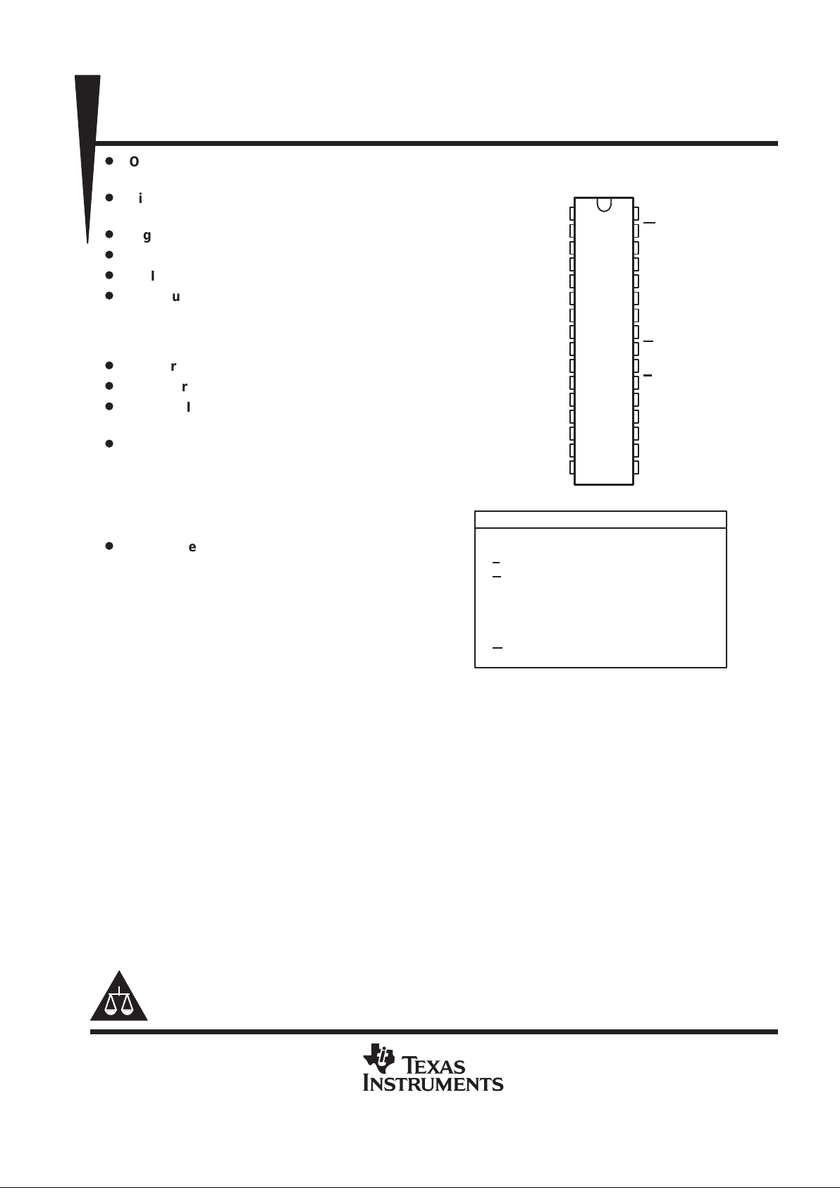
The SMJ28F010B flash memory is offered in a 32-lead ceramic 600-mil side-braze dual in-line package (DIP)
(JDD suffix) and a leadless ceramic chip carrier (FE suffix).
Please be aware that an important notice concerning availability, standard warranty, and use in critical applications of
Texas Instruments semiconductor products and disclaimers thereto appears at the end of this data sheet.
A0–A16 Address Inputs
DQ0–DQ7 Inputs (programming)/Outputs
E Chip Enable
G
Output Enable
NC No Internal Connection
V
CC
5-V Power Supply
V
PP
12-V Power Supply
V
SS
Ground
W
Write Enable
PIN NOMENCLATURE
JDD or FE PACKAGE
(TOP VIEW)
1
2
3
4
5
6
7
8
9
10
11
12
13
14
15
16
32
31
30
29
28
27
26
25
24
23
22
21
20
19
18
17
V
PP
A16
A15
A12
A7
A6
A5
A4
A3
A2
A1
A0
DQ0
DQ1
DQ2
V
SS
V
CC
W
NC
A14
A13
A8
A9
A1 1
G
A10
E
DQ7
DQ6
DQ5
DQ4
DQ3
Copyright 1998, Texas Instruments Incorporated
On products compliant to MIL-PRF-38535, all parameters are tested
unless otherwise noted. On all other products, production
processing does not necessarily include testing of all parameters.
PRODUCTION DATA information is current as of publication date.
Products conform to specifications per the terms of Texas Instruments
standard warranty. Production processing does not necessarily include
testing of all parameters.
Page 2

SMJ28F010B
131072 BY 8-BIT
FLASH MEMORY
SGMS738 – APRIL 1998
2
POST OFFICE BOX 1443 • HOUSTON, TEXAS 77251–1443
device symbol nomenclature
Temperature Range Designator
M=–55°C to 125°C
Package Designator
JDD = Ceramic Side-Braze
Dual- In-Line Package
Speed Designator
-12 = 120 ns
-15 = 150 ns
-20 = 200 ns
-12 JDD MSMJ28F010B
Page 3
SMJ28F010B
131072 BY 8-BIT
FLASH MEMORY
SGMS738 – APRIL 1998
3
POST OFFICE BOX 1443 • HOUSTON, TEXAS 77251–1443
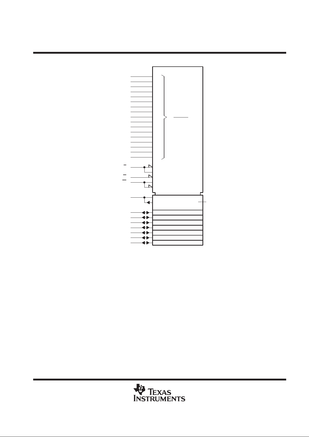
logic symbol
†
A
0
131 071
FLASH
MEMORY
131 072 × 8
16
0
G1
[PWR DWN]
G2
1, 2 EN (READ)
1C3 (WRITE)
A, 3D
∇ 4
A0
A1
A2
A3
A4
A5
A6
A7
A8
A9
A10
A11
A12
A13
A14
A15
A16
E
G
W
DQ0
DQ1
DQ2
DQ3
DQ4
DQ5
DQ6
DQ7
12
11
10
9
8
7
6
5
27
26
23
25
4
28
29
3
2
22
24
31
13
14
15
17
18
19
20
21
A, Z4
†
This symbol is in accordance with ANSI/IEEE Std 91-1984 and IEC Publication 617-12.
Pin numbers shown are for the JDD package.
Page 4
SMJ28F010B
131072 BY 8-BIT
FLASH MEMORY
SGMS738 – APRIL 1998
4
POST OFFICE BOX 1443 • HOUSTON, TEXAS 77251–1443
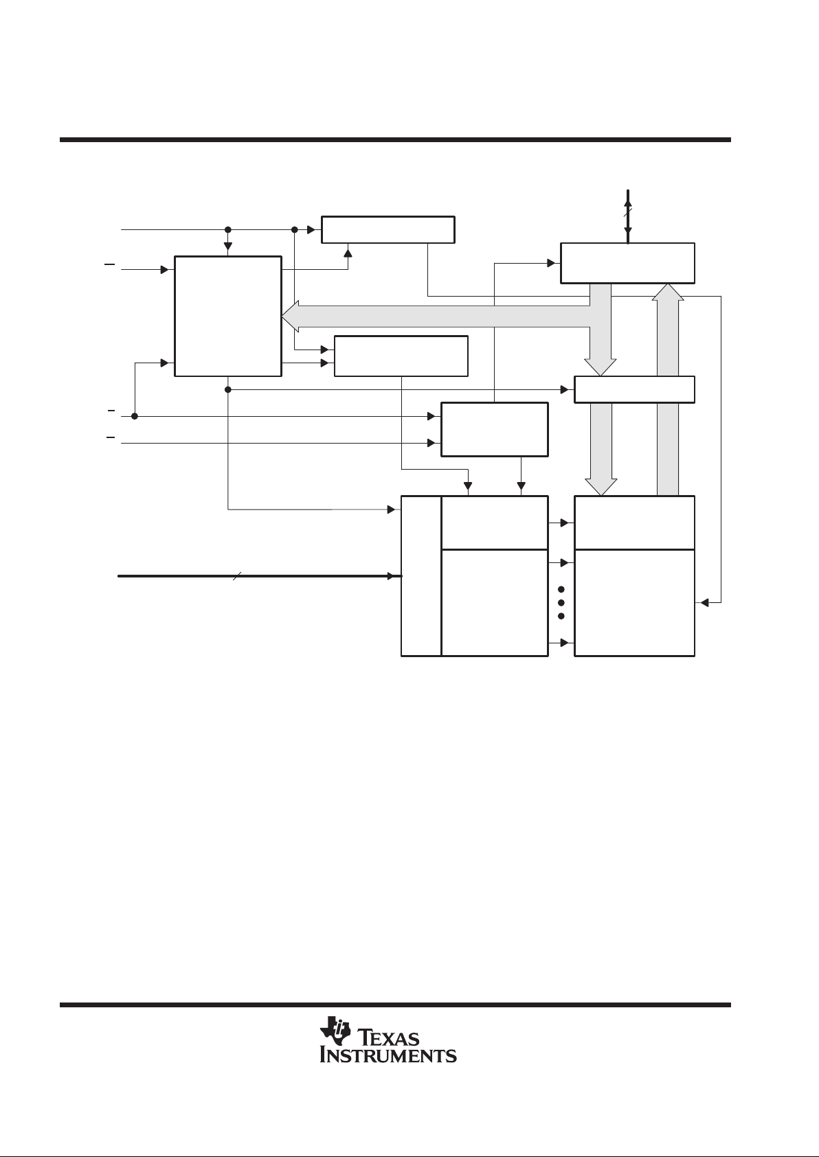
functional block diagram
Erase-Voltage Switch
V
PP
A0–A16
A
d
d
r
e
s
s
L
a
t
c
h
Column Decoder
Row Decoder
Chip-Enable and
Output-Enable
Logic
DQ0–DQ7
Program-Voltage
Switch
W
1048576-Bit
Array Matrix
To Array
STB
STB
Input/Output Buffers
E
G
State Control
Program/Erase
Stop Timer
Command Register
Data Latch
Column Gating
8
17
Page 5
SMJ28F010B
131072 BY 8-BIT
FLASH MEMORY
SGMS738 – APRIL 1998
5
POST OFFICE BOX 1443 • HOUSTON, TEXAS 77251–1443
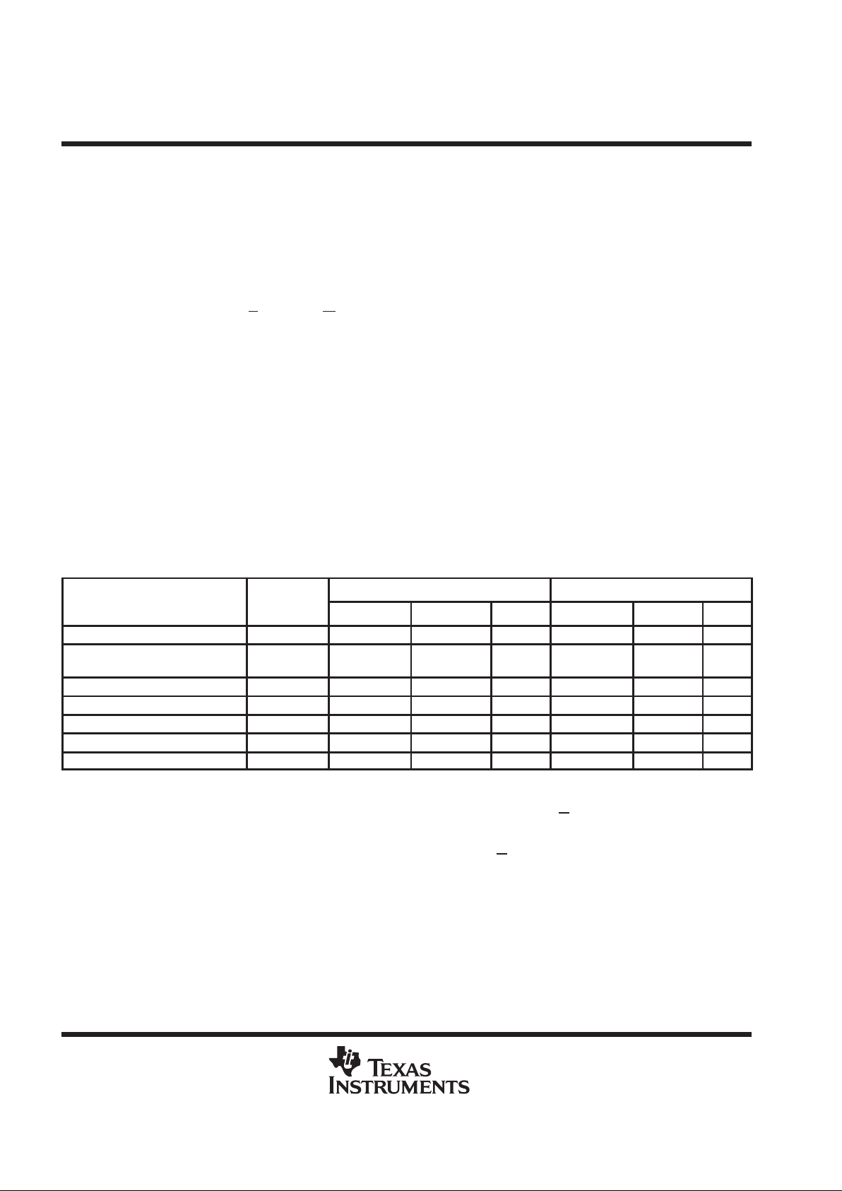
operation
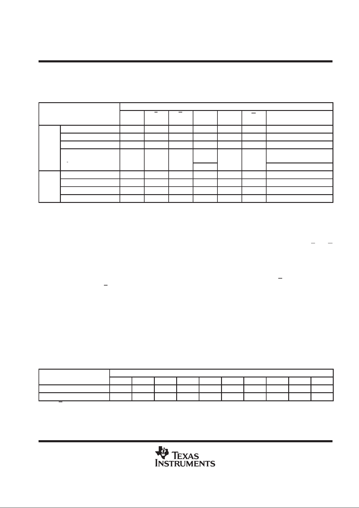
Table 1 lists the modes of operation for the device.
Table 1. Operation Modes
FUNCTION
†
MODE
V
PP
‡
(1)
E
(22)
G
(24)
A0
(12)
A9
(26)
W
(31)
DQ0–DQ7
(13–15, 17–21)
Read V
PPL
V
IL
V
IL
X X
V
IH
Data Out
Output Disable V
PPL
V
IL
V
IH
X X
V
IH
Hi-Z
Standby and Write Inhibit V
PPL
V
IH
X X X
X
Hi-Z
Read
Algorithm-Selection Mode V
V
V
V
IL
V
V
Manufacturer-Equivalent
Code 89h
g
PPLILIL
V
IH
ID
IH
Device-Equivalent Code B4h
Read V
PPH
V
IL
V
IL
X X
V
IH
Data Out
Read/
Output Disable V
PPH
V
IL
V
IH
X X
V
IH
Hi-Z
Write
Standby and Write Inhibit V
PPH
V
IH
X X X
X
Hi-Z
Write V
PPH
V
IL
V
IH
X X
V
IL
Data In
†
X can be VIL or VIH.
‡
V
PPL
≤ VCC + 2 V; V
PPH
is the programming voltage specified for the device. For more details, see the recommended operating conditions.
read/output disable
When the outputs of two or more SMJ28F010B devices are connected in parallel on the same bus, the output
of any particular device in the circuit can be read with no interference from the competing outputs of other
devices. Reading the output of the SMJ28F010B is enabled when a low-level signal is applied to the E
and G
pins. All other devices in the circuit must have their outputs disabled by applying a high-level signal to one of
these pins.
standby and write inhibit
Active I
CC
current can be reduced from 30 mA to 1 mA by applying a high TTL level on E or to 100 µA with a
high CMOS level on E
. In this mode, all outputs are in the high-impedance state. The SMJ28F010B draws active
current when it is deselected during programming, erasure, or program/erase verification. It continues to draw
active current until the operation is terminated.
algorithm-selection mode
The algorithm-selection mode provides access to a binary code identifying the correct programming and erase
algorithms. This mode is activated when A9 ( pin 26) is forced to V
ID
. Two identifier bytes are accessed by
toggling A0. All other addresses must be held low.
A0 low selects the manufacturer-equivalent code 89h, and
A0 high selects the device-equivalent code B4h, as shown in Table 2.
Table 2. Algorithm-Selection Modes
PINS
IDENTIFIER
§
A0 DQ7 DQ6 DQ5 DQ4 DQ3 DQ2 DQ1 DQ0 HEX
Manufacturer-Equivalent Code V
IL
1 0 0 0 1 0 0 1 89
Device-Equivalent Code V
IH
1 0 1 1 0 1 0 0 B4
§
E =VIL, G = VIL, A1–A8 = VIL, A9 = VID, A10–A16 = VIL, VPP = V
PPL
.
Page 6
SMJ28F010B
131072 BY 8-BIT
FLASH MEMORY
SGMS738 – APRIL 1998
6
POST OFFICE BOX 1443 • HOUSTON, TEXAS 77251–1443
programming and erasure
In the erased state, all bits are at a logic 1. Before erasing the device, all memory bits must be programmed to
a logic 0. Then the entire chip is erased. At this point, the bits, which are now logic 1s, can be programmed
accordingly. See the fast-write and fast-erase algorithms for further details.
command register
The command register controls the program and erase functions of the SMJ28F010B. The algorithm-selection
mode can be activated using the command register in addition to the previously described method. When V
PP
is high, the contents of the command register and the function being performed can be changed. The command
register is written to when E
is low and W is pulsed low. The address is latched on the leading edge of the pulse,
while the data is latched on the trailing edge. Accidental programming or erasure is minimized because two
commands must be executed to invoke either operation. The command register is inhibited when V
CC
is below
the erase/write lockout voltage, V
LKO
.
power-supply considerations
Each device must have a 0.1-µF ceramic capacitor connected between V
CC
and VSS to suppress circuit noise.
Changes in current drain on V
PP
require it to have a bypass capacitor as well. Printed-circuit traces for both
power supplies should be appropriate to handle the current demand.
command definitions
The commands include read, algorithm-selection mode, set-up-erase, erase, erase-verify, set-up-program,
program, program-verify, and reset. Table 3 lists the command definitions with the required bus cycles.
Table 3. Command Definitions
REQUIRED
FIRST BUS CYCLE SECOND BUS CYCLE
COMMAND
BUS
CYCLES
OPERATION†ADDRESS DATA OPERATION†ADDRESS DATA
Read 1 Write X 00h Read RA RD
Algorithm-Selection Mode 3 Write X 90h Read
0000h
0001h
89h
B4h
Set-Up-Erase/Erase 2 Write X 20h Write X 20h
Erase-Verify 2 Write EA A0h Read X EVD
Set-Up-Program/Program 2 Write X 40h Write PA PD
Program-Verify 2 Write X C0h Read X PVD
Reset 2 Write X FFh Write X FFh
Legend:
EA Address of memory location to be read during erase verify
RA Address of memory location to be read
PA Address of memory location to be programmed. Address is latched on the falling edge of W
.
RD Data read from location RA during the read operation
EVD Data read from location EA during erase verify
PD Data to be programmed at location PA. Data is latched on the rising edge of W
.
PVD Data read from location PA during program verify
†
Modes of operation are defined in Table 1.
read command
Memory contents can be accessed while V
PP
is high or low. When VPP is high, writing 00h into the command
register invokes the read operation. When the device is powered up, the default contents of the command
register are 00h and the read operation is enabled. The read operation remains enabled until a different
command is written to the command register.
Page 7

SMJ28F010B
131072 BY 8-BIT
FLASH MEMORY
SGMS738 – APRIL 1998
7
POST OFFICE BOX 1443 • HOUSTON, TEXAS 77251–1443
algorithm-selection mode command
The algorithm-selection mode is activated by writing 90h into the command register. The device-equivalent code
(B4h) is identified by the value read from address location 0001h, and the manufacturer-equivalent code (89h)
is identified by the value read from address location 0000h.
set-up-erase/erase commands
The erase-algorithm initiates with E
= VIL, W = VIL, G = VIH, VPP = V
PPH
, and VCC = 5 V . T o enter the erase mode,
write the set-up-erase command, 20h, into the command register. After the SMJ28F010B is in the erase mode,
writing a second erase command, 20h, into the command register invokes the erase operation. The erase
operation begins on the rising edge of W
and ends on the rising edge of the next W. The erase operation requires
at least 9.5 ms to complete before the erase-verify command, A0h, can be loaded.
Maximum erase timing is controlled by the internal stop timer. When the stop timer terminates the erase
operation, the device enters an inactive state and remains inactive until a command is received.
program-verify command
The SMJ28F010B can be programmed sequentially or randomly , because it is programmed one byte at a time.
Each byte must be verified after it is programmed. The program-verify operation prepares the device to verify
the most recently programmed byte. To invoke the program-verify operation, C0h must be written into the
command register. The program-verify operation ends on the rising edge of W
.
While verifying a byte, the SMJ28F010B applies an internal margin voltage to the designated byte. If the true
data and programmed data match, programming continues to the next designated byte location; otherwise, the
byte must be reprogrammed. Figure 1 shows how commands and bus operations are combined for byte
programming.
erase-verify command
All bytes must be verified following an erase operation. After the erase operation is complete, an erased byte
can be verified by writing the erase-verify command, A0h, into the command register. This command causes
the device to exit the erase mode on the rising edge of W
. The address of the byte to be verified is latched on
the falling edge of W
. The erase-verify operation remains enabled until a command is written to the command
register.
T o determine whether all the bytes have been erased, the SMJ28F010B applies a margin voltage to each byte.
If FFh is read from the byte, all bits in the designated byte have been erased. The erase-verify operation
continues until all of the bytes have been verified. If FFh is not read from a byte, an additional erase operation
needs to be executed. Figure 2 shows the combination of commands and bus operations for electrically erasing
the SMJ28F010B.
set-up-program/program commands
The programming algorithm initiates with E
= VIL, W = VIL, G = VIH, VPP = V
PPH
, and VCC = 5 V . To enter the
programming mode, write the set-up-program command, 40h, into the command register. The programming
operation is invoked by the next write-enable pulse. Addresses are latched internally on the falling edge of W
,
and data is latched internally on the rising edge of W
. The programming operation begins on the rising edge
of W
and ends on the rising edge of the next W pulse. The program operation requires 10 µs for completion
before the program-verify command, C0h, can be loaded.
Maximum program timing is controlled by the internal stop timer. When the stop timer terminates the program
operation, the device enters an inactive state and remains inactive until a command is received.
reset command
To reset the SMJ28F010B after set-up-erase-command or set-up-program-command operations without
changing the contents in memory, perofrm two consecutive writes of FFh into the command register. After
executing the reset command, the device defaults to the read mode.
Page 8

SMJ28F010B
131072 BY 8-BIT
FLASH MEMORY
SGMS738 – APRIL 1998
8
POST OFFICE BOX 1443 • HOUSTON, TEXAS 77251–1443
fast-write algorithm
Figure 1 shows the process flow for programming the SMJ28F010B. The fast-write algorithm programs in a
nominal time of two seconds.
fast-erase algorithm
Figure 2 shows the process flow for erasing the SMJ28F010B using the fast-erase algorithm. The memory array
must be completely programmed (using the fast-write algorithm) before erasure begins. Erasure typically
occurs in one second.
parallel erasure
Several devices can be erased in parallel, reducing total erase time. Since the rate at which each flash memory
can erase differs, every device must be verified separately after each erase pulse. After a given device has been
successfully erased, the erase command should not be reissued to this device. All devices that complete
erasure should be masked until the parallel erasure process is finished (see Figure 3).
Examples of how to mask a device during parallel erase include driving the E
pin high, writing the read command
(00h) to the device when the others receive a set-up-erase or erase command, and disconnecting the device
from all electrical signals with relays or other types of switches.
flow charts
Figure 1, Figure 2, and Figure 3 are flow charts showing the fast-write algorithm, the fast-erase algorithm, and
the parallel-erase flow.
Page 9

SMJ28F010B
131072 BY 8-BIT
FLASH MEMORY
SGMS738 – APRIL 1998
9
POST OFFICE BOX 1443 • HOUSTON, TEXAS 77251–1443
flow charts (continued)
Bus
Operation
Command Comments
Initialize
Address
Standby
Wait for VPP to ramp to
V
PPH
(see Note A)
Initialize pulse count
Write
Set-UpProgram
Write
Data = 40h
Write
Write Data Valid address/data
Standby
Wait = 10 µs
Write
ProgramVerify
Data = C0h; ends
program operation
Standby
Wait = 6 µs
Read
Read byte to verify
programming; compare
output to expected output
—
— —
Write
Read Data = 00h; resets register
for read operations
Standby
Wait for VPP to ramp to
V
PPL
(see Note B)
NOTES: A. See the recommended operating conditions for the value of V
PPH.
B. See the recommended operating conditions for the value of V
PPL
.
Figure 1. Algorithm-Selection Programming Flow Chart
Apply V
PPL
Last
Address
?
Start
Address = 00h
VCC = 5 V ± 10%, VPP = 12 V ± 5%
Device Passed
Increment
Address
Read
and Verify
Byte
Pass
No
Yes
Yes
No
Fail
X = 1
Write Data
X = X + 1
Wait = 10µs
Write Read Command
X = 25?
Setup
Wait = 6 µs
Write Program-Verify Command
Device Failed
Power
Down
Interactive
Mode
Apply V
PPL
Write Set-Up-Program Command
Page 10

Write Erase-Verify Command
Setup
Last
Address?
Start
Increment
Address
Read
and Verify
Byte
X = X + 1
Wait = 10 ms
Pass
Write Read Command
X = 1000?
All Bytes = 00h
Interactive
Mode
Write-Erase Command
Program All
Bytes to 00h
Apply V
PPL
Power
Down
Apply V
PPL
Address = 00h
VCC = 5 V ± 10%, VPP = 12 V ± 5%
X = 1
Device Passed Device Failed
No
Yes
No
Yes
Fail
No
Yes
Wait = 6 µs
Preprogram
?
Write Set-Up-Erase Command
SMJ28F010B
131072 BY 8-BIT
FLASH MEMORY
SGMS738 – APRIL 1998
10
POST OFFICE BOX 1443 • HOUSTON, TEXAS 77251–1443
flow charts (continued)
Bus
Operation
Command Comments
Entire memory must = 00h
before erasure
Use fast-write
programming algorithm
Initialize addresses
Standby
Wait for VPP to ramp to
V
PPH
(see Note A)
Initialize pulse count
Write
Set-UpErase
Data = 20h
Write
Erase Data = 20h
Standby
Wait = 10 ms
Write
EraseVerify
Addr = Byte to verify;
Data = A0h; ends the erase
operation
Standby
Wait = 6 µs
Read
Read byte to verify erasure;
compare output to FFh
Write
Read Data = 00h; resets register
for read operations
Standby
Wait for VPP to ramp to
V
PPL
(see Note B)
NOTES: A. Refer to the recommended operating conditions for the value of V
PPH.
B. Refer to the recommended operating conditions for the value of V
PPL
.
Figure 2. Flash-Erase Flow Chart
Page 11

SMJ28F010B
131072 BY 8-BIT
FLASH MEMORY
SGMS738 – APRIL 1998
11
POST OFFICE BOX 1443 • HOUSTON, TEXAS 77251–1443
flow charts (continued)
Start
Program All Devices to 00h
Give Erase Command to All
Devices
D = n
†
?
All Devices Pass
No
Yes
Is
Device #D
Erased
?
Yes
No
Mask Device #D
X = 1
Device # D = 1
D = D+1
Are
All Devices
Erased
?
No
Yes
X = X+1
Give Erase
Command to
All Unmasked
Devices
No
X = 1000
?
Yes
Give Read
Command to
All Devices
Give Read
Command to
All Devices
Finished With Errors
†
n = number of devices being erased.
Figure 3. Parallel-Erase Flow Chart
Page 12

SMJ28F010B
131072 BY 8-BIT
FLASH MEMORY
SGMS738 – APRIL 1998
12
POST OFFICE BOX 1443 • HOUSTON, TEXAS 77251–1443
absolute maximum ratings over operating free-air temperature range (unless otherwise noted)
†
Supply voltage range, V
CC
(see Note 1) –0.6 V to 7 V. . . . . . . . . . . . . . . . . . . . . . . . . . . . . . . . . . . . . . . . . . . . . .
Supply voltage range, V
PP
–0.6 V to 14 V. . . . . . . . . . . . . . . . . . . . . . . . . . . . . . . . . . . . . . . . . . . . . . . . . . . . . . . . .
Input voltage range (see Note 2): All inputs except A9 –0.6 V to 7 V. . . . . . . . . . . . . . . . . . . . . . . . . . . . . . . . . .
A9 –0.6 V to 13.5 V. . . . . . . . . . . . . . . . . . . . . . . . . . . . . . . . . . . . . . . . . . . . . . .
Output voltage range (see Note 3) –0.6 V to 7 V. . . . . . . . . . . . . . . . . . . . . . . . . . . . . . . . . . . . . . . . . . . . . . . . . . .
Output short-circuit current (see Note 4) 200mA. . . . . . . . . . . . . . . . . . . . . . . . . . . . . . . . . . . . . . . . . . . . . . . . . . .
Operating free-air temperature range during read/erase/program, T
A
–55°C to 125°C. . . . . . . . . . . . . . . . .
Storage temperature range, T
stg
–65°C to 150°C. . . . . . . . . . . . . . . . . . . . . . . . . . . . . . . . . . . . . . . . . . . . . . . . . . .
Maximum power dissipation, P
D
1 W. . . . . . . . . . . . . . . . . . . . . . . . . . . . . . . . . . . . . . . . . . . . . . . . . . . . . . . . . . . . .
Lead temperature (soldering, 10 seconds) 300°C. . . . . . . . . . . . . . . . . . . . . . . . . . . . . . . . . . . . . . . . . . . . . . . . . .
Junction temperature, T
J
150°C. . . . . . . . . . . . . . . . . . . . . . . . . . . . . . . . . . . . . . . . . . . . . . . . . . . . . . . . . . . . . . . . . .
†
Stresses beyond those listed under “absolute maximum ratings” may cause permanent damage to the device. These are stress ratings only, and
functional operation of the device at these or any other conditions beyond those indicated under “recommended operating conditions” is not
implied. Exposure to absolute-maximum-rated conditions for extended periods may affect device reliability.
NOTES: 1. All voltage values are with respect to VSS.
2. The voltage on any input pin can undershoot to –2 V for periods less than 20 ns.
3. The voltage on any output pin can overshoot to 7 V for periods less than 20 ns.
4. No more than one output can be shorted at a time, and the duration cannot exceed one second.
recommended operating conditions
MIN NOM MAX UNIT
V
CC
Supply voltage During write/read/flash erase 4.5 5 5.5 V
pp
During read only (V
PPL
) 0 VCC + 2 V
VPPSuppl
y v
oltage
During write/read/flash erase (V
PPH
) 11.4 12 12.6 V
p
TTL 2 VCC+0.5
VIHHigh-level dc input voltage
CMOS VCC– 0.5 VCC+0.5
V
p
TTL –0.5 0.8
VILLow-level dc input voltage
CMOS GND – 0.2 GND+0.2
V
V
ID
Voltage level on A9 for algorithm-selection mode 11.5 13 V
T
A
Operating free-air temperature –55 125 °C
Page 13

SMJ28F010B
131072 BY 8-BIT
FLASH MEMORY
SGMS738 – APRIL 1998
13
POST OFFICE BOX 1443 • HOUSTON, TEXAS 77251–1443
electrical characteristics over recommended ranges of supply voltage and operating free-air
temperature (unless otherwise noted)
PARAMETER TEST CONDITIONS MIN MAX UNIT
p
VCC = 4.5 V, IOH = – 2.5 mA 2.4
VOHHigh-level output voltage
VCC = 4.5 V, IOH = – 100 µA VCC– 0.4
V
p
VCC = 4.5 V, IOL = 5.8 mA 0.45
VOLLow-level output voltage
IOL = 100 µA 0.1
V
I
ID
A9 algorithm-selection-mode current VCC = 5.5 V, A9 = VID max 200* µA
p
All except A9 VCC = 5.5 V, VI = 0 V to 5.5 V ±1
IIInput current (leakage)
A9 VCC = 5.5 V, VI = 0 V to 13 V ± 200
µ
A
I
O
Output current (leakage) VCC = 5.5 V, VO = 0 V to V
CC
±10 µA
pp
VPP = V
PPH
, Read mode 200
I
PP1
V
PP
supply current (read/standby)
VPP = V
PPL
±10
µ
A
I
PP2
VPP supply current (during program pulse) VPP = V
PPH
30* mA
I
PP3
VPP supply current (during flash erase) VPP = V
PPH
30* mA
I
PP4
VPP supply current (during program/erase-verify) VPP = V
PPH
5.0* mA
pp
TTL-input level VCC = 5.5 V, E = V
IH
1 mA
I
CCSVCC
su
pply current (standby)
CMOS-input level VCC = 5.5 V, E = VCC ± 0.2 V 100 µA
I
CC1VCC
supply current (active read)
VCC = 5.5 V, E = VIL,
f = 6 MHz, I
OUT
= 0 mA,
G
= V
IH
30 mA
I
CC2VCC
average supply current (active write)
VCC = 5.5 V, E = VIL,
Programming in progress
10* mA
I
CC3VCC
average supply current (flash erase)
VCC = 5.5 V, E = VIL,
Erasure in progress
15* mA
I
CC4VCC
average supply current (program/erase-verify)
VCC = 5.5 V, E = VIL,
VPP = V
PPH
,
Program/erase-verify in progress
15* mA
V
LKOVCC
erase/write-lockout voltage VPP = V
PPH
2.5 V
* This parameter is not production tested.
capacitance over recommended range of supply voltage
PARAMETER TEST CONDITIONS MIN MAX UNIT
C
i1
Input capacitance
VI = 0 V, TA = 25°C,
f = 1 MHz
10* pF
C
o
Output capacitance
VO = 0 V, TA = 25°C,
f = 1 MHz
12* pF
C
i2VPP
input capacitance
VI = 0 V, TA = 25°C,
f = 1 MHz
12* pF
* This parameter is not production tested.
Page 14

SMJ28F010B
131072 BY 8-BIT
FLASH MEMORY
SGMS738 – APRIL 1998
14
POST OFFICE BOX 1443 • HOUSTON, TEXAS 77251–1443
switching characteristics over recommended ranges of supply voltage and operating free-air
temperature (see Figure 6)
TEST ALTERNATE
’28F010B-12 ’28F010B-15 ’28F010B-20
PARAMETER
CONDITIONS SYMBOL
MIN MAX MIN MAX MIN MAX
UNIT
t
a(A)
Access time from address,
A0–A16
t
AVQV
120 150 200 ns
t
a(E)
Access time from chip enable, E t
ELQV
120 150 200 ns
t
en(G)
Access time from output
enable, G
t
GLQV
50 55 60 ns
t
c(R)
Cycle time, read t
AVAV
120 150 200 ns
t
d(E)
Delay time, E low to low-Z
output
CL = 100 pF,
1 Series 74
t
ELQX
0* 0* 0* ns
t
d(G)
Delay time, G low to low-Z
output
TTL load
,
Input tr ≤ 10 ns,
Input tf ≤ 10 ns
t
GLQX
0* 0* 0* ns
t
dis(E)
Chip disable time to Hi-Z output
f
t
EHQZ
0* 55* 0* 55* 0* 55* ns
t
dis(G)
Output disable time to Hi-Z
output
t
GHQZ
0* 30* 0* 35* 0* 45* ns
t
h(D)
Hold time, data valid from
address, E
or G (see Note 5)
t
AXQX
0* 0* 0* ns
t
rec(W)
Recovery time, W before read t
WHGL
6 6 6 µs
* This parameter is not production tested.
NOTE 5: Whichever occurs first
Page 15

SMJ28F010B
131072 BY 8-BIT
FLASH MEMORY
SGMS738 – APRIL 1998
15
POST OFFICE BOX 1443 • HOUSTON, TEXAS 77251–1443
timing requirements–write/erase/program operations (see Figure 7 and Figure 8)
ALTERNATE
’28F010B-12 ’28F010B-15 ’28F010B-20
SYMBOL
MIN NOM MAX MIN NOM MAX MIN NOM MAX
UNIT
t
c(W)
Cycle time, write
using W
t
AVAV
120 150 200 ns
t
c(W)PR
Cycle time, programming operation
t
WHWH1
10 10 10 µs
t
c(W)ER
Cycle time, erase
operation
t
WHWH2
9.5 10 9.5 10 9.5 10 ms
t
h(A)
Hold time, address t
WLAX
60 60 60 ns
t
h(E)
Hold time, E t
WHEH
0 0 0 ns
t
h(WHD)
Hold time, data valid
after W
high
t
WHDX
10 10 10 ns
t
su(A)
Setup time, address t
AVWL
0 0 0 ns
t
su(D)
Setup time, data t
DVWH
50 50 50 ns
t
su(E)
Setup time, E before
W
t
ELWL
20 20 20 ns
t
su(VPPEL)
Setup time, VPP to E
low
t
VPEL
1 1 1 µs
t
rec(W)
Recovery time, W
before read
t
WHGL
6 6 6 µs
t
rec(R)
Recovery time, read
before W
t
GHWL
0 0 0 µs
t
w(W)
Pulse duration, W
(see Note 6)
t
WLWH
60 60 60 ns
t
w(WH)
Pulse duration, W
high
t
WHWL
20 20 20 ns
t
r(VPP)
Rise time, V
PP
t
VPPR
1 1 1 µs
t
f(VPP)
Fall time, V
PP
t
VPPF
1 1 1 µs
NOTE 6: Rise/fall time ≤ 10 ns.
Page 16

SMJ28F010B
131072 BY 8-BIT
FLASH MEMORY
SGMS738 – APRIL 1998
16
POST OFFICE BOX 1443 • HOUSTON, TEXAS 77251–1443
timing requirements — alternative E-controlled writes (see Figure 9)
’
’
’
ALTERNATE
’28F010B-12
’28F010B-15
’28F010B-20
SYMBOL
MIN MAX MIN MAX MIN MAX
UNIT
t
c(W)
Cycle time, write using E t
AVAV
120 150 200 ns
t
c(E)PR
Cycle time, programming operation t
EHEH
10 10 10 µs
t
h(EA)
Hold time, address t
ELAX
80 80 80 ns
t
h(ED)
Hold time, data t
EHDX
10 10 10 ns
t
h(W)
Hold time, W t
EHWH
0 0 0 ns
t
su(A)
Setup time, address t
AVEL
0 0 0 ns
t
su(D)
Setup time, data t
DVEH
50 50 50 ns
t
su(W)
Setup time, W before E t
WLEL
0 0 0 ns
t
su(VPPEL)
Setup time, VPP to E low t
VPEL
1 1 1 µs
t
rec(E)R
Recovery time, write using E before read t
EHGL
6 6 6 µs
t
rec(E)W
Recovery time, read before write using E t
GHEL
0 0 0 µs
t
w(E)
Pulse duration, write using E t
ELEH
70 70 70 ns
t
w(EH)
Pulse duration, write, E high t
EHEL
20 20 20 ns
PARAMETER MEASUREMENT INFORMATION
2.08 V
CL = 100 pF
(see Note A)
Output
Under Test
RL = 800 Ω
NOTE A: CL includes probe and fixture capacitance.
Figure 4. AC Test Output Load Circuit
2.4 V
0.45 V
2 V
0.8 V
2 V
0.8 V
See Note A
NOTE A: The ac testing inputs are driven at 2.4 V for logic high and 0.45 V for logic low. Timing measurements are made at 2 V for logic high
and 0.8 V for logic low on both inputs and outputs. Each device should have a 0.1-µF ceramic capacitor connected between VCC and
VSS as closely as possible to the device pins.
Figure 5. AC Test Input/Output Waveform
Page 17

SMJ28F010B
131072 BY 8-BIT
FLASH MEMORY
SGMS738 – APRIL 1998
17
POST OFFICE BOX 1443 • HOUSTON, TEXAS 77251–1443
PARAMETER MEASUREMENT INFORMATION
A0–A16
E
G
W
DQ0–DQ7 Ouput Valid
Address Valid
t
d(E)
t
d(G)
t
c(R)
t
a(A)
t
a(E)
t
dis(E)
t
rec(W)
t
en(G)
t
dis(G)
t
h(D)
Hi-Z Hi-Z
Figure 6. Read-Cycle Timing
Page 18

SMJ28F010B
131072 BY 8-BIT
FLASH MEMORY
SGMS738 – APRIL 1998
18
POST OFFICE BOX 1443 • HOUSTON, TEXAS 77251–1443
PARAMETER MEASUREMENT INFORMATION
0 V
Power Up
and
Standby
Set-Up-
Program
Command
Program
Command
Latch
Address
and Data
Programming
Program
Verify
Command
Program
Verification
Standby/
Power Down
A0–A16
E
G
W
DQ0–DQ7
t
h(D)
t
w(W)
t
su(D)
t
a(E)
t
su(VPPEL)
t
h(WHD)
Data In = 40h
Data In
Data In = C0h
Valid Data Out
t
h(A)
t
h(E)
5 V
V
CC
V
PPH
V
PP
V
PPL
t
r(VPP)
t
w(WH)
t
c(W)PR
t
h(A)
t
dis(E)
t
dis(G)
t
d(E)
t
su(E)
t
h(E)
t
su(E)
t
su(E)
t
h(E)
t
h(WHD)
t
rec(R)
t
h(WHD)
t
w(W)
t
su(D)
t
w(W)
t
su(D)
t
en(G)
t
c(W)
t
su(A)
t
su(A)
t
c(R)
t
f(VPP)
t
rec(W)
t
c(W)
t
c(W)
t
d(G)
Hi-Z
Figure 7. Write-Cycle Timing
Page 19

SMJ28F010B
131072 BY 8-BIT
FLASH MEMORY
SGMS738 – APRIL 1998
19
POST OFFICE BOX 1443 • HOUSTON, TEXAS 77251–1443
PARAMETER MEASUREMENT INFORMATION
Power Up
and
Standby
Set-Up-
Erase
Command
Erase
Command
Erasing
Erase-
Verify
Command
Erase
Verification
Standby/
Power Down
A0–A16
E
G
W
DQ0–DQ7
5 V
V
CC
0 V
V
PPH
V
PP
V
PPL
t
dis(G)
t
h(D)
t
h(WHD)
t
w(W)
t
su(D)
t
d(E)
t
a(E)
t
su(VPPEL)
t
h(WHD)
Data In = 20h
Data In = 20h
Data In = A0h
Valid Data Out
t
h(A)
t
su(E)
t
r(VPP)
t
f(VPP)
t
dis(E)
t
d(G)
t
en(G)
t
w(W)
t
su(D)
t
h(E)
t
h(E)
t
h(E)
t
w(WH)
t
su(E)
t
rec(R)
t
h(WHD)
t
su(A)
Hi-Z
t
w(W)
t
su(D)
t
c(W)
t
c(R)
t
c(W)ER
t
rec(W)
t
c(W)
t
su(E)
t
c(W)
Figure 8. Flash-Erase-Cycle Timing
Page 20

SMJ28F010B
131072 BY 8-BIT
FLASH MEMORY
SGMS738 – APRIL 1998
20
POST OFFICE BOX 1443 • HOUSTON, TEXAS 77251–1443
PARAMETER MEASUREMENT INFORMATION
Power Up
and
Standby
Set-Up-
Program
Command
Program
Command
Latch
Address
and Data
Programming
Program
Verify
Command
Program
Verification
Standby/
Power Down
A0–A16
W
G
E
DQ0–DQ7
t
dis(G)
t
dis(E)
t
h(D)
t
a(E)
t
su(VPPEL)
Data In = 40h
Data In
Data In = C0h
Valid Data Out
t
su(W)
t
h(EA)
t
h(W)
t
h(W)
t
h(ED)
V
PPH
V
PP
V
PPL
t
r(VPP)
t
f(VPP)
t
h(W)
t
h(EA)
t
w(E)
t
su(D)
t
w(E)
t
h(ED)
t
su(D)
t
rec(E)W
t
w(E)
t
su(D)
t
su(W)
t
su(W)
t
en(G)
t
w(EH)
t
c(E)PR
t
h(ED)
t
c(W)
t
su(A)
t
d(E)
5 V
V
CC
0 V
t
su(A)
t
c(W)
t
c(W)
t
c(R)
t
d(G)
t
rec(E)R
Hi-Z
Figure 9. Write-Cycle (Alternative E-Controlled Writes) Timing
Page 21

SMJ28F010B
131072 BY 8-BIT
FLASH MEMORY
SGMS738 – APRIL 1998
21
POST OFFICE BOX 1443 • HOUSTON, TEXAS 77251–1443
MECHANICAL DATA
FE (R-CQCC-N**) LEADLESS CERAMIC CHIP CARRIER
4040137/B 03/95
0.045 (1,14)
0.045 (1,14)
0.025 (0,64)
0.025 (0,64)
0.022 (0,56)
0.045 (1,14)
0.028 (0,71)
0.028 (0,71)
0.055 (1,40)
0.035 (0,89)
0.035 (0,89) 0.015 (0,38)
0.015 (0,38)
A
127 3
1317
26 4
18 12
28 TERMINAL SHOWN
C
NO. OF
TERMINALS
18
28
32
(11,30) (11,56)
0.445 0.455
(8,76) (9,02)
0.345 0.355
(7,24) (7,49)
0.285 0.295
MIN
A
(13,72) (14,22)
0.540 0.560
(13,72) (14,22)
0.540 0.560
(8,76) (9,27)
0.345 0.365
MIN
C
**
MAXMAX
(1,65) (2,01)
0.065 0.079
(1,65) (2,01)
0.065 0.079
(1,55) (1,85)
0.061 0.073
MIN
B
MAX
B
0.050 (1,27)
NOTES: A. All linear dimensions are in inches (millimeters).
B. This drawing is subject to change without notice.
C. This package can be hermetically sealed with a metal lid.
D. The terminals are gold plated.
Page 22

SMJ28F010B
131072 BY 8-BIT
FLASH MEMORY
SGMS738 – APRIL 1998
22
POST OFFICE BOX 1443 • HOUSTON, TEXAS 77251–1443
MECHANICAL DATA
JDD (R-CDIP-T32) CERAMIC SIDE-BRAZE DUAL-IN-LINE PACKAGE
4040280/B 03/96
17
16
0.060 (1,52)
0.030 (0,76)
0.605 (15,37)
0.585 (14,86)
0.590 (14,99)
0.610 (15,49)
0.125 (3,18)
0.175 (4,45)
Seating Plane
0.008 (0,20)
0.014 (0,36)
0.045 (1,14)
0.065 (1,65)
1.580 (40,13)
1.620 (41,15)
32
1
0.089 (2,26)
0.120 (3,05)
0.021 (0,53)
0.015 (0,38)
0.100 (2,54)
NOTES: A. All linear dimensions are in inches (millimeters).
B. This drawing is subject to change without notice.
C. This package can be hermetically sealed with a metal lid.
D. The terminals will be gold plated.
Page 23

IMPORTANT NOTICE
T exas Instruments (TI) reserves the right to make changes to its products or to discontinue any semiconductor
product or service without notice, and advises its customers to obtain the latest version of relevant information
to verify, before placing orders, that the information being relied on is current and complete.
TI warrants performance of its semiconductor products and related software to the specifications applicable at
the time of sale in accordance with TI’s standard warranty. Testing and other quality control techniques are
utilized to the extent TI deems necessary to support this warranty. Specific testing of all parameters of each
device is not necessarily performed, except those mandated by government requirements.
Certain applications using semiconductor products may involve potential risks of death, personal injury, or
severe property or environmental damage (“Critical Applications”).
TI SEMICONDUCTOR PRODUCTS ARE NOT DESIGNED, INTENDED, AUTHORIZED, OR WARRANTED
TO BE SUITABLE FOR USE IN LIFE-SUPPORT APPLICATIONS, DEVICES OR SYSTEMS OR OTHER
CRITICAL APPLICATIONS.
Inclusion of TI products in such applications is understood to be fully at the risk of the customer. Use of TI
products in such applications requires the written approval of an appropriate TI officer. Questions concerning
potential risk applications should be directed to TI through a local SC sales office.
In order to minimize risks associated with the customer’s applications, adequate design and operating
safeguards should be provided by the customer to minimize inherent or procedural hazards.
TI assumes no liability for applications assistance, customer product design, software performance, or
infringement of patents or services described herein. Nor does TI warrant or represent that any license, either
express or implied, is granted under any patent right, copyright, mask work right, or other intellectual property
right of TI covering or relating to any combination, machine, or process in which such semiconductor products
or services might be or are used.
Copyright 1998, Texas Instruments Incorporated
 Loading...