

Page 1
Austin Semiconductor, Inc.
UVEPROM
SMJ27C040
4 MEG UVEPROM
UV Erasable Programmable
Read-Only Memory
A V AILABLE AS MILIT AR Y
SPECIFICA TIONS
• SMD 5962-91752
• MIL-STD-883
FEATURES
• Organized 524,288 x 8
• Single +5V ±10% power supply
• Industry standard 32-pin dual-in-line package
• All inputs/outputs fully TTL compatible
• Static Operation (no clocks, no refresh)
• 8-bit output for use in microprocessor-based systems
• Power-saving CMOS technology
• 3-state output buffers
• 400-mV DC assured noise immunity with standarad
TTL loads
• Latchup immunity of 250 mA on all input and output
pins
• No pullup resistors required
• Low power dissipation (Vcc = 5.5V)
PActive - 385 mW Worst Case
PStandby - 0.55 mW Worst Case (CMOS-input levels)
OPTIONS MARKING
• Timing
120ns access -1 2
150ns access -1 5
• Package(s)
Ceramic DIP (600mils) J No. 114
• Operating Temperature Ranges
Military (-55oC to +125oC) M
For more products and information
please visit our web site at
www.austinsemiconductor .com
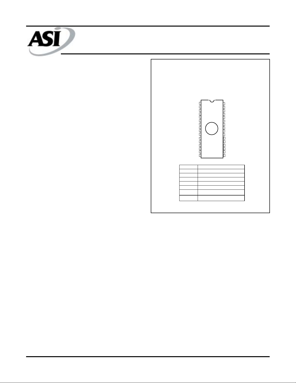
PIN ASSIGNMENT
(Top View)
32-Pin DIP (J)
(600 MIL)
1
V
PP
2
A16
3
A15
4
A12
5
A7
6
A6
7
A5
8
A4
9
A3
10
A2
11
A1
12
A0
13
DQ0
14
DQ1
15
DQ2
16
GND
Pin Name Function
A0 - A18 Address Inputs
DA0-DQ7 Inputs (programming)/Outputs
E\ Chip Enable
G\ Output Enable
GND Ground
V
5V Supply
CC
V
13V Power Supply*
PP
*Only in program mode.
Vcc
32
A18
31
A17
30
A14
29
A13
28
A8
27
A9
26
A11
25
G\
24
A10
23
22
E\
21
DQ7
20
DQ6
19
DQ5
18
DQ4
17
DQ3
GENERAL DESCRIPTION
The SMJ27C040 is a set of 4,194,304-bit, ultraviolet-light
erasable, electrically programmable read-only memories
(EPROMs).
These devices are fabricated using CMOS technology for
high speed and simple interface with MOS and bipolar
circuits. All inputs (including program data inputs) can be
driven by Series 54 TTL circuits. Each output can drive one
Series 54 TTL circuit without external resistors. The data
outputs are 3-state for connecting multiple devices to a
common bus.
The SMJ27C040 is offered in a 32-pin 600-mil
dual-in-line ceramic package (J suffix) rated for operation
from -55°C to 125°C.
Since this EPROM operates from a single 5V supply (in
the read mode), it is ideal for use in microprocessor-based
systems. One other (13V) supply is needed for programming.
All programming signals are TTL level. For programming
outside the system, existing EPROM programmers can be
used.
SMJ27C040
Rev. 1.0 9/01
Austin Semiconductor, Inc. reserves the right to change products or specifications without notice.
1
Page 2
Austin Semiconductor, Inc.
FUNCTIONAL BLOCK DIAGRAM*
EPROM 524,288 x 8
12
A0
11
A1
10
A2
A3
8
A4
A5 DQ0
6
A6 DQ1
A7 DQ2
27
A8 DQ3
26
A9 DQ4
23
A10 DQ5
25
A11 DQ6
4
A12 DQ7
28
A13
29
A14
3
A15
2
A16
30
A17
31
A18
22
E\
G\
24
[PWR DWN]
&
A
EN
0
524,287
A
A
A
A
A
A
A
A
UVEPROM
SMJ27C040
13
14
15
17
18
19
20
21
* This symbol is in accordance with ANSI/IEEE std 91-1984 and IEC Publication 617-12. Pin numbers shown are for the J package.
OPERATION
The seven modes of operation are listed in Table 1. The read mode requires a single 5V supply. All inputs are TTL level
except for VPP during programming (13V), and VH (12V)i on A9 for signature mode.
T ABLE 1. OPERA TION MODES
FUNCTION
V
CC
V
CC
V
CC
V
CC
V
CC
V
CC
V
CC
CC
Austin Semiconductor, Inc. reserves the right to change products or specifications without notice.
A9 A0 DQ0-DQ7
X X Data Out
X X High-Z
X X High-Z
X X Data In
X X High-Z
X X Data Out
V
V
*Signature Mode V
IH
IL
V
IL
MFG Code 97
Device Code 50
2
Read
Output Disable
Standby
Programming
Program Inhibit
Verify
* X can be VIL or VIH.
iVH = 12V ± 0.5V
SMJ27C040
Rev. 1.0 9/01
E\ G\
V
IL
V
IL
V
IH
V
IL
V
IH
V
IH
V
IL
V
PP
V
IL
V
IH
X
V
IH
V
IH
V
IL
V
IL
V
CC
V
CC
V
CC
V
PP
V
PP
V
PP
V
CC
Page 3

Austin Semiconductor, Inc.
UVEPROM
SMJ27C040
READ/OUTPUT DISABLE
When the outputs of two or more SMJ27C040s are connected
in parallel on the same bus, the output of any particular device
in the circuit can be read with no interference from
competing outputs of the other devices. T o read the output of
a single device, a low level signal is applied to the E\ and G\
pins. All other devices in the circuit should have their outputs
disabled by applying a high level signal to one of these pins.
Output data is accessed at pins Q0-Q7.
LA TCHUP IMMUNITY
Latchup immunity on the SMJ27C040 is a minimum of 250mA
on all inputs and outputs. This feature provides latchup
immunity beyond any potential transients at the P .C. board level
when the EPROM is interfaced to industry standard TTL or
MOS logic devices. The input/output layout approach
controls latchup without compromising performance or
packing density .
POWER DOWN
Active ICC supply current can be reduced from 70mA to 1mA
for a high TTL input on E\ and to 100µA for a high CMOS
input on E\. In this mode all outputs are in the highimpedance state.
ERASURE
Before programming, the SMJ27C040 EPROM is erased by
exposing the chip through the transparent lid to a high
intensity ultraviolet-light (wavelength 2537 Å). The
recommended minimum exposure dose (UV intensity x
exposure time) is 15-W.s/cm2. A typical 12-mW/cm2,
filterless UV lamp erases the device in 21 minutes. The lamp
should be located about 2.5cm above the chip during erasure.
After erasure, all bits are in the high state. It should be noted
that normal ambient light contains the correct wavelength for
erasure. Therefore, when using the SMJ27C040, the window
should be covered with an opaque label. After erasure (all
bits in logic high state), logic lows are programmed into the
desired locations. A programmed low can be erased only by
ultraviolet light.
SNAP! PULSE PROGRAMMING
The SMJ27C040 is programmed by using the SNAP! Pulse
programming algorithm. The programming sequence is shown
in the SNAP! Pulse programming flow chart (Figure 1).
The initial setup is V
= 13V, V
PP
= 6.5V, E\ = VIH, and
CC
G\ = VIL. Once the initial location is selected, the data is
presented in parallel (eight bits) on pins DQ1 through DQ8.
Once addresses and data are stable, the programming mode is
achieved when E\ is pulsed low (VIL) with a pulse duration of
t
. Every location is programmed only once before
W(PGM)
going to interactive mode.
In the interactive mode, the word is verified at V
= 13V,
PP
VCC= 6.5V, E\ = VIH, and G\ = VIL. If the correct data is not
read, the programming is performed by pulling G\ high, then
E\ low with a pulse duration of t
. This sequence of
W(PGM)
verification and programming is performed up to a maximum
of 10 times. When the device is fully programmed, all bytes
are verified with VCC = VPP = 5V ± 10%.
PROGRAM INHIBIT
Programming can be inhibited by maintaining high level
inputs on the E\ and G\ pins.
PROGRAM VERIFY
Programmed bits can be verified with VPP = 13V when
G\ = VIL, and E\ = VIH.
SIGNA TURE MODE
The signature mode provides access to a binary code
identifying the manufacturer and type. This mode is activated
when A9 (pin 26) is forced to 12V. Two identifier bytes are
accessed by toggling A0. All other addresses must be held
low. The signature code for the SMJ27C040 is 9750. A0 low
selects the manufacturer’s code 97 (Hex), and A0 high
selects the device code 50 (Hex), as shown in Table 2.
TABLE 2. SIGNATURE MODES
IDENTIFIER*
MANUFACTURER CODE
DEVICE CODE
* E\ = G\ = VIL, A1 - A8 = VIL, A9 = VH, A10 - A18 = VIL, VPP = VCC.
SMJ27C040
Rev. 1.0 9/01
A0 DQ7 DQ6 DQ5 DQ4 DQ3 DQ2 DQ1 DQ0 HEX
V
IL
V
IH
1001011197
0101000050
3
PINS
Austin Semiconductor, Inc. reserves the right to change products or specifications without notice.
Page 4
UVEPROM
SMJ27C040
Austin Semiconductor, Inc.
FIGURE 1. SNAP! PULSE PROGRAMMING FLOW CHART
START
Address = First Location
Increment
Address
VCC = 6.5V ± 0.25V, VPP = 13V ± 0.25V
Program One Pulse = tW = 100µs
Last
Address?
Yes
Address = First Location
X = 0
Verify
One
Byte
Pass
Fail
Increment Address
Program One Pulse = tW = 100µs
No
X = X+1
X = 10?
Program
Mode
Interactive
Mode
SMJ27C040
Rev. 1.0 9/01
No
VCC = VPP = 5V ± 0.5V
Last
Address?
Yes
Compare
All Bytes
to Original
Data
Pass
Device Passed
Fail
Yes
Device Failed
Final
Verification
Austin Semiconductor, Inc. reserves the right to change products or specifications without notice.
4
Page 5

Austin Semiconductor, Inc.
UVEPROM
SMJ27C040
ABSOLUTE MAXIMUM RATINGS*
Supply Voltage Range, VCC**...........................-0.6V to +7.0V
Supply Voltage Range, Vpp**.........................-0.6V to +14.0V
Input Voltage Range, All inputs except A9**..-0.6V to +6.5V
A9.....-0.6V to +13.0V
Output Voltage Range,
with respect to VSS**..................................-0.6V to VCC +1
*Stresses greater than those listed under "Absolute Maximum
Ratings" may cause permanent damage to the device. This is
a stress rating only and functional operation of the device at
these or any other conditions above those indicated in the
operation section of this specification is not implied.
Exposure to absolute maximum rating conditions for extended
periods may affect reliability.
** All voltage values are with respect to GND.
Minimum Operating Free-air Temperature.....................-55°C
Maximum Operating Case T emperature.........................125°C
Storage Temperature Range.............................-65°C to 150°C
RECOMMENDED OPERA TING CONDITIONS
V
V
Supply Voltage
CC
Supply Voltage
PP
Read Mode
SNAP! Pulse programming algorithm
Read Mode
SNAP! Pulse programming algorithm
1
2
TTL 2
High-level input voltageV
IH
V
T
T
NOTES:
1. VCC must be applied before or at the same time as VPP and removed after or at the same time as VPP. The deivce must not be inserted into or removed from the
board when VPP or VCC is applied.
2. VPP can be connected to VCC directly (except in the program mode). VCC supply current in this case would be ICC + IPP. During programming, VPP must be
maintained at 13V ± 0.25V .
Low-level input voltage
IL
Operating free-air temperature
A
Operating case temperature
C
CMOS
TTL -0.5 0.8 V
CMOS -0.5 0.2 V
MIN TYP MAX UNIT
4.5 5 5.5 V
6.25 6.5 6.75 V
-0.6 VCC+0.6
V
CC
12.75 13 13.25 V
+0.5
V
CC
-0.2 VCC+0.5
V
CC
-55 °C
+125 °C
V
V
V
ELECTRICAL CHARACTERISTICS O VER RECOMMENDED RANGES OF SUPPLY V OL TA GE AND
OPERA TING FREE-AIR TEMPERA TURE
PARAMETER
V
V
I
I
I
I
NOTES:
1. This parameter is only sampled and not 100% tested.
2. Minimum cycle time = maximum access time.
SMJ27C040
Rev. 1.0 9/01
High-level output voltage
OH
Low-level output voltage
OL
Input current (leakage)
I
I
Output current (leakage)
I
O
supply current
V
PP1
PP2
CC1
CC2
PP
V
supply current (during program pulse)
PP
VCC supply current (standby)
supply current (active)
V
CC
1
TTL-Input Level
CMOS-Input Level
TEST CONDITIONS MIN MAX UNIT
IOH = -400µA
IOL = 2.1mA
VI = 0V to 5.5V
VO = 0V to V
VPP = VCC = 5.5V
VPP = 12.75V, TA -25°C
V
= 5.5V, E\=V
CC
V
= 5.5V, E\=V
CC
E\=VIL, VCC=5.5V
= minimum cycle time,
t
cycle
outputs open
CC
IH
CC
2
Austin Semiconductor, Inc. reserves the right to change products or specifications without notice.
2.4 V
100 µA
5
0.4 V
±1 µA
±1 µA
10 µA
50 mA
1mA
50 mA
Page 6

UVEPROM
SMJ27C040
Austin Semiconductor, Inc.
CAP A CIT ANCE O VER RECOMMENDED RANGES OF SUPPLY V OL TA GE AND OPERATING
FREE-AIR TEMPERATURE, f = 1MHz (VCC = VPP = 5V ±0.5V)*
PARAMETER
C
C
* Capacitance is sampled only at initial design and after any major change.
** All typical values are at T
Input capacitance
i
Output capacitance
o
= 25°C and nominal voltages.
A
SWITCHING CHARACTERISTICS O VER RECOMMENDED RANGES OF SUPPLY V OL TAGE
AND OPERA TING FREE-AIR TEMPERATURE
PARAMETER
Access time from address 120 150 ns
t
a(A)
Access time from chip enable 120 150 ns
t
a(E)
t
NOTES:
1. V alue calculated from 0.5V delta to measured output level. This parameter is only sampled and not 100% tested.
2. Common test conditions apply for t
3. For all switching characteristics the input pulse levels are 0.4V to 2.4V . T iming measurements are made at 2V for logic high and 0.8V for logic low . (Figure 2)
Output enable time from G\ 50 50 ns
en(G)
Output disable time from G\ or E\, whichever
t
dis
occurs first
Output data valid time after change of
t
v(A)
address, E\, or G\, whichever occurs first
1
dis
TEST CONDITIONS TYP** MAX UNIT
= 0V
V
I
= 0V
V
O
1
except during programming.
CONDITIONS
(see Figure 2)
Input t
Input t
48pF
812pF
1,2
TEST
2, 3
< 20ns
r
< 20ns
f
-12
MIN MAX MIN MAX
050050 ns
00 ns
-15
UNIT
SWITCHING CHARACTERISTICS FOR PROGRAMMING: VCC = 6.5V and VPP = 13V (SNAP!
Pulse), TA = 25°C
MIN MAX UNIT
t
dis(G)
t
en(G)
PARAMETER
Output disable time from G\ 0 100 ns
Output enable time from G\ 150 ns
TIMING REQUIREMENTS FOR PROGRAMMING
MIN TYP MAX UNIT
t
h(A)
t
h(D)
t
w(PGM)
t
su(A)
t
su(E)
t
su(G)
t
su(D)
t
su(Vpp)
t
su(Vcc)
SMJ27C040
Rev. 1.0 9/01
Hold Time, Address
Hold Time, Data
Pulse Duration, Program SNAP! Pulse Programming Algorithm 95 100 105 µs
Setup Time, Address
Setup Time, E\
Setup Time, G\
Setup Time, Data
Setup Time, V
Setup Time, V
PP
CC
Austin Semiconductor, Inc. reserves the right to change products or specifications without notice.
6
0µs
2µs
2µs
2µs
2µs
2µs
2µs
2µs
Page 7

Austin Semiconductor, Inc.
P ARAMETER MEASUREMENT INFORMATION
2.08V
RL = 800Ω
Output Under Test
UVEPROM
SMJ27C040
NOTES:
1. CL includes probe and fixture capacitance.
FIGURE 2. OUTPUT LOAD CIRCUIT AND INPUT/OUTPUT W AVE FORMS
CL = 100 pF
1
FIGURE 3. READ-CYCLE TIMING
SMJ27C040
Rev. 1.0 9/01
Austin Semiconductor, Inc. reserves the right to change products or specifications without notice.
7
Page 8

UVEPROM
SMJ27C040
Austin Semiconductor, Inc.
FIGURE 4. PROGRAM-CYCLE TIMING (SNAP! PULSE PROGRAMMING)
* 13V VPP and 6.5V VCC for SNAP! Pulse programming.
SMJ27C040
Rev. 1.0 9/01
Austin Semiconductor, Inc. reserves the right to change products or specifications without notice.
8
Page 9

Austin Semiconductor, Inc.
MECHANICAL DEFINITION*
ASI Case #114 (Package Designator J)
SMD 5962-91752, Case Outline X
UVEPROM
SMJ27C040
Pin 1
D
e
E
E1
b2
SMD Specifications
SYMBOL
MIN MAX
A --- 0.225
b 0.014 0.026
b1 0.045 0.065
b2 0.008 0.018
D --- 1.680
E 0.510 0.620
e
E1
0.100 BSC
0.600 BSC
L1 0.125 0.200
L 0.015 0.070
A
L
L1
b
b1
NOTE: These dimensions are per the SMD. ASI's package dimensional limits
may differ, but they will be within the SMD limits.
*All measurements are in inches.
SMJ27C040
Rev. 1.0 9/01
Austin Semiconductor, Inc. reserves the right to change products or specifications without notice.
9
Page 10

Austin Semiconductor, Inc.
ORDERING INFORMATION
UVEPROM
SMJ27C040
EXAMPLE:
Device
Number
SMJ27C040 -12 J *
SMJ27C040 -15 J *
SMJ27C040-15JM
Speed ns
Package
Type
Operating
Temp.
*A V AILABLE PROCESSES
M = Extended T emperature Range -55oC to +125oC
SMJ27C040
Rev. 1.0 9/01
Austin Semiconductor, Inc. reserves the right to change products or specifications without notice.
10
Page 11

Austin Semiconductor, Inc.
ASI TO DSCC PART NUMBER
CROSS REFERENCE*
ASI Pac kage Designator J
TI Part #** SMD Part #
SMJ27C040-12JM 5962-9175205MXA
SMJ27C040-15JM 5962-9175204MXA
UVEPROM
SMJ27C040
* ASI part number is for reference only. Orders received referencing the SMD part number will be processed per the SMD.
** Parts are listed on SMD under the old Texas Instruments part number. ASI purchased this product line in November of 1999.
SMJ27C040
Rev. 1.0 9/01
11
Austin Semiconductor, Inc. reserves the right to change products or specifications without notice.
 Loading...