

Datasheet SMH4803AHMP, SMH4803AHN, SMH4803AHNP, SMH4803AJK, SMH4803AJKP Datasheet (SUMMIT)
...Page 1
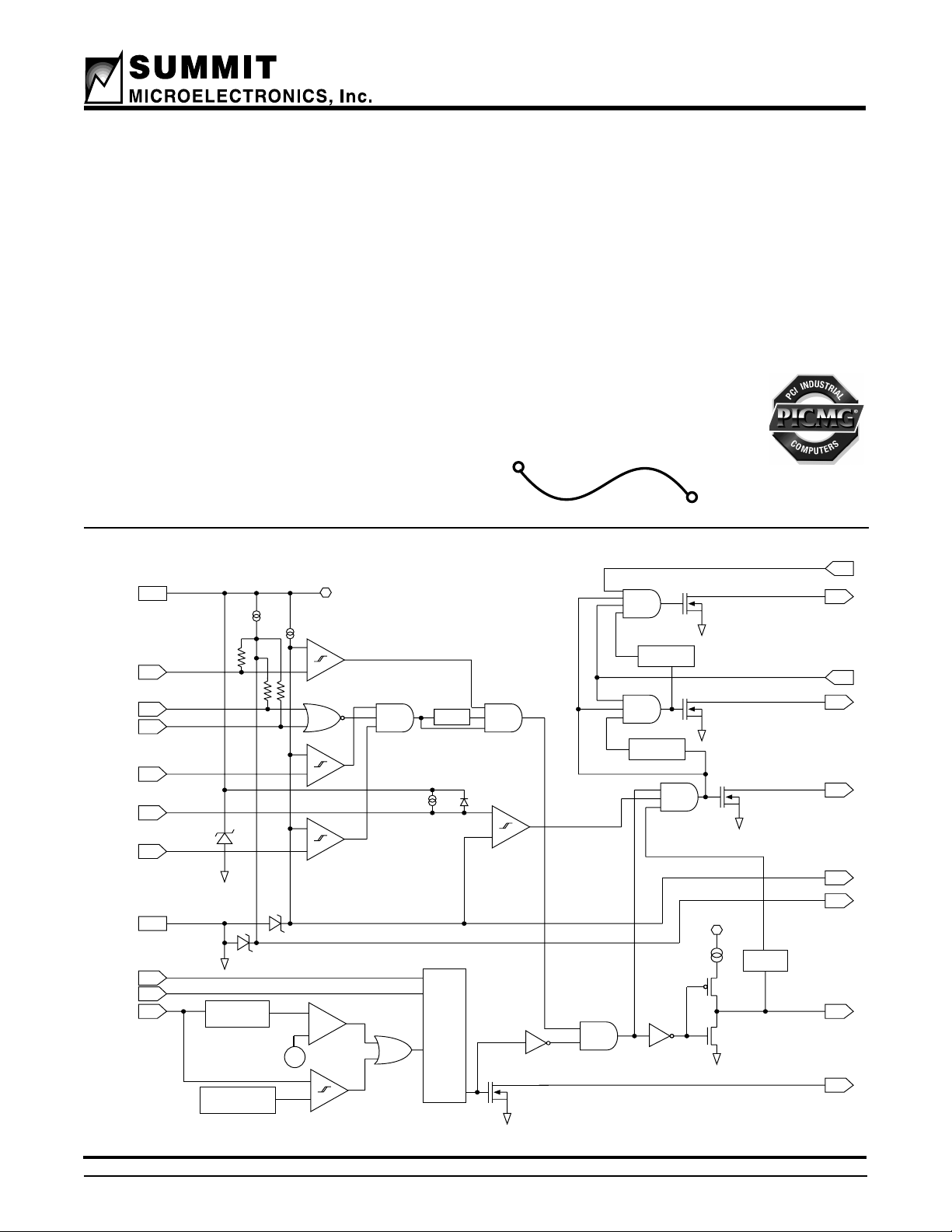
Distributed Power Hot-Swap Controller
FEATURES
• Supply Range ±20VDC to >±500VDC
• Versatile Card Insertion Detection Supports
Both
– Multi-length Pin Systems
– Card Injector Switch Sensing
• Control Up to Four Loads or a Primary Load and
3 DC/DC Converters
• Highly
–
•
Programmable
Sequencing DC/DC Converters
FUNCTIONAL BLOCK DIAGRAM
Programmable
Programmable
Detection
Power Good Delays for
Host Voltage Monitoring
Under- and Over-voltage
•
Programmable
–
Programmable
Programmable
–
Circuit Breaker Function
Over-current Filter
Quick-Trip™ Circuit Breaker
Values
–
Programmable
Circuit Breaker Mode
• Duty-Cycle Mode
• Latched Mode
• 2.5V and 5.0V reference outputs
– Easy Expansion of External
Monitor Functions
eaturing
F
k
c
i
-
u
T
r
P
r
o
g
r
a
m
C
Q
e
l
b
a
e
m
r
B
t
i
u
c
r
i
i
p
TM
e
r
k
a
SMH4803
ASSOCIATE
MEMBER
VDD
EN/TS
PD1#
PD2#
Drain
Sense
CBMode
CBReset#
CBSense
UV
OV
VSS
50kΩ
Programmable
Programmable
Quick-Trip
Ref Voltage
50kΩ
12V
Delay
ENPGB
12V ref
-
+
50kΩ
Filter
-
+
+
-
2.5V
5V
+
-
50
mV
+
-
Fault
Latch
&
Duty
Cycle
Timer
-
+
Programmable
Delay
Programmable
Delay
current limit
12V
Vgate
Sense
PG3#
ENPGA
PG2#
PG1#
2.5V ref
5.0V ref
Vgate
CBFault#
2041 BD 8.0
© SUMMIT MICROELECTRONICS, Inc. 2000 • 300 Orchard City Drive, Suite 131 • Campbell, CA 95008 • Telephone 408-378-6461 • Fax 408-378-6586 • www.summitmicro.com
2041 8.4 6/15/00
1
Characteristics subject to change without notice
Page 2
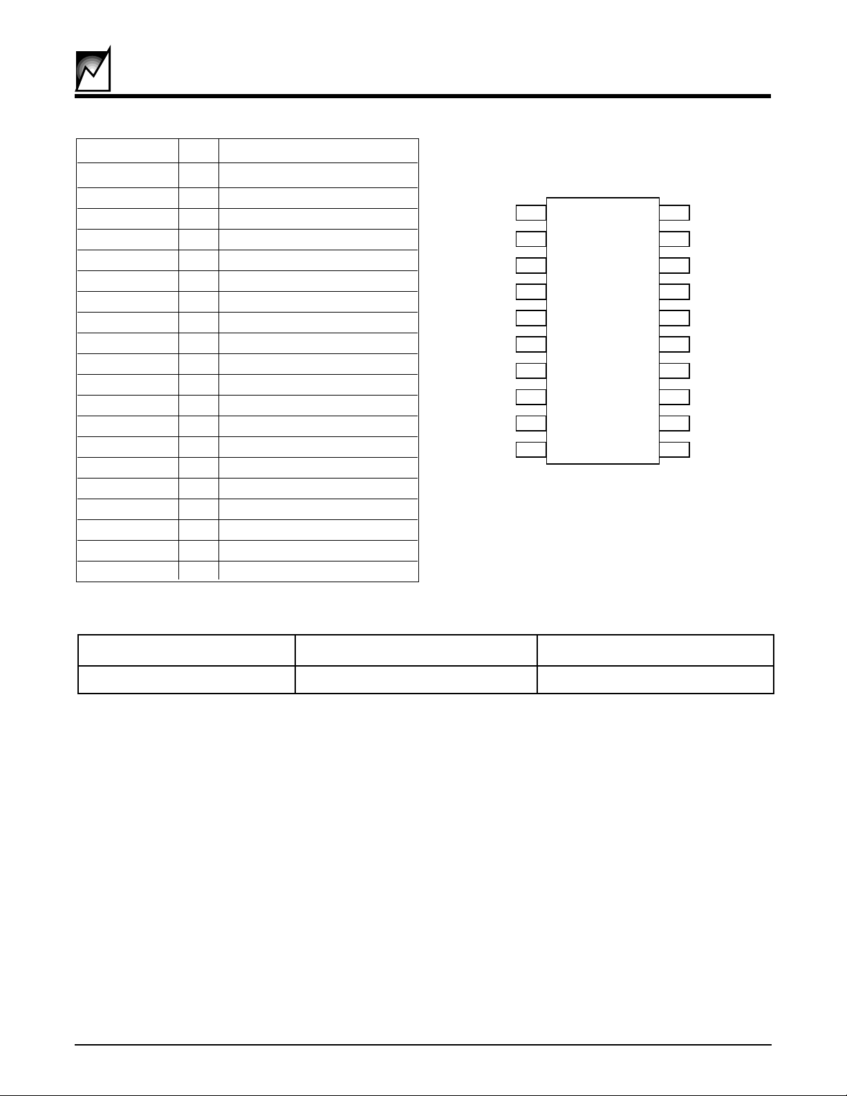
SMH4803
Symbol Pin Description
Drain Sense 1 Drain sense input
Vgate 2 Output to MOSFET gate
EN/TS 3 Enable/Temp Sense input
PD1# 4 Pin Detect 1 (active LO)
PD2# 5 Pin Detect 2 (active LO)
CBFault# 6 Circuit Breaker Fault output
CBReset# 7 Circuit Breaker Reset intput
CBMode 8 Circuit Breaker Mode control
CBSense 9 Cicruit Breaker Sense input
Vss 10 Negative Supply Connection
UV 11 Under Voltage input
OV 12 Over Voltage input
5V 13 5V reference output
2.5V 14 2.5V reference output
ENPGB 15 Enable input B
ENPGA 16 Enable input A
PG3# 17 Power good output 3
PG1# 18 Power good output 1
PG2# 19 Power good output 2
Vdd 20 Positive supply connection
2041 PGM T2.1
PIN CONFIGURATIONS
Drain Sense
Vgate
EN/TS
PD1#
PD2#
CBFault#
CBReset#
CBMode
CBSense
Vss
1
2
3
4
5
6
7
8
9
10
20
19
18
17
16
15
14
13
12
11
Vdd
PG2#
PG1#
PG3#
ENPGA
ENPGB
2.5V
5V
OV
UV
2041 ILL10.1
RECOMMENDED OPERATING CONDITIONS
Condition Min Max
Temperature -40°C +85°C
DESCRIPTION
The SMH4803 is designed to control hot swapping of
plug-in cards operating from a single supply ranging from
20V to 500V. The SMH4803 hot-swap controller provides
under-voltage and over-voltage monitoring of the host
power supply, it drives an external power MOSFET switch
that connects the supply to the load, and also protects
against over-current conditions that might disrupt the host
supply. When the input and output voltages to the
SMH4803 controller are within specification, the
SMH4803 provides three “Power Good” logic outputs that
2041 PGM T3.0
may be used to turn ON the loads, e.g. isolated-output DCDC converters, or drive LED status lights. The SMH4803
provides three separate “Power Good” logic outputs that
activate loads in a timed sequence. Additional features of
the SMH4803 include: temperature sense or master enable input, 2.5V and 5V reference outputs for expanding
monitor functions, two “Pin-Detect” enable inputs for fault
protection, and duty-cycle or latched over-current protection modes.
2041 8.4 6/15/00
2
SUMMIT MICROELECTRONICS
Page 3
SMH4803
ABSOLUTE MAXIMUM RATINGS
Temperature Under Bias -55°C to +125°C
Storage Temperature -65°C to +150°C
Voltage on pins with respect to V
UV, OV, CBSense, Drain Sense -0.5V to Vdd +0.5V
PD1#, PD2#, CBMode, CBReset# 10V
ENPGA, ENPGB, EN/TS
CBFault#, PG1#, PG2#, PG3# -0.5V to Vdd +0.5V
Lead Solder Temperature (10 secs) 300 °C
SS
Vdd -0.5V to Vdd
Vgate Vdd + 0.5V
DC OPERATING CHARACTERISTICS (Over Recommended Operating Conditions, Voltages are relative to V
*COMMENT
Stresses listed under Absolute Maximum Ratings
may cause permanent damage to the device. These
are stress ratings only, and functional operation of
the device at these or any other conditions outside
those listed in the operational sections of this specification is not implied. Exposure to any absolute
maximum rating for extended periods may affect
device performance and reliability.
SS
Symbol Parameter Notes Min. Typ. Max. Units
V
DD
Supply Voltage IDD = 2mA 11 12 13 V
Vref5 5Volt Reference Output IDD = 2mA 4.7 5 5 5.25 V
I
LOAD5
5Volt Reference Output Current IDD = 2mA -1 1 mA
Vref2.5 2.5 Volt Reference Output TA = 25 °C, IDD = 2mA 2.475 2.5 2.525 V
Vref2.5 2.5 Volt Reference Output IDD = 2mA 2.425 2.5 2.575 V
I
LOAD2.5
I
DD
V
UV
V
UV
V
UVHYS
V
OV
V
OV
V
OVHYS
V
VGATE
I
VGATE
V
SENSE
V
SENSE
I
SENSE
V
CB
V
QCB
V
ENTS
V
ENTS
V
ENTSHYS
V
IH
2.5 Volt Reference Output Current IDD = 2mA -0.2 1 mA
Power Supply Current Output Enabled 2 10 mA
Under voltage Threshold TA = 25 °C, IDD = 2mA 2.475 2.5 2.525 V
Under voltage Threshold IDD = 2mA 2.425 2.5 2.575 V
Under voltage Hysteresis IDD = 2mA 10 mV
Over voltage Threshold TA = 25 °C, IDD = 2mA 2.475 2.5 2.525 V
Over voltage Threshold IDD = 2mA 2.425 2.5 2.575 V
Over voltage Hysteresis IDD = 2mA 10 mV
Vgate Output Voltage V
DD
Vgate Current Output 100 µ A
Drain Sense threshold TA = 25 °C, IDD = 2mA 2.475 2.5 2.525 V
Drain Sense threshold IDD = 2mA 2.425 2.5 2.575 V
Drain Sense Output Current (Note 1) V
SENSE
= V
SS
91011µA
Circuit Breaker Threshold IDD = 2mA 40 50 60 mV
Quick-Trip Circuit Breaker Threshold
Option E
Option F
Option H
Option J
200 mV
100 mV
50 mV
OFF
EN/TS Threshold TA = 25 °C, IDD = 2mA 2.425 2.5 2.575 V
EN/TS Threshold IDD = 2mA 2.475 2.5 2.525 V
EN/TS Hysteresis IDD = 2mA 5 10 15 mV
Input High Voltage ENPGA/B, 2 Vref5 V
CBMode, CBReset#
V
IL
Input High Voltage ENPGA/B, -0.1 0.8 V
CBMode, CBReset#
V
OL
V
OL
CBFault# Output Low Voltage IOL = 2mA 0 0.4 V
PG1#, PG2#, PG3# Output Low I
= 2mA 0 0.4 V
SINK
)
V
(Note 1) : TA = 25 °C
SUMMIT MICROELECTRONICS
2041 PGM T4.4
3
2041 8.4 6/15/00
Page 4
SMH4803
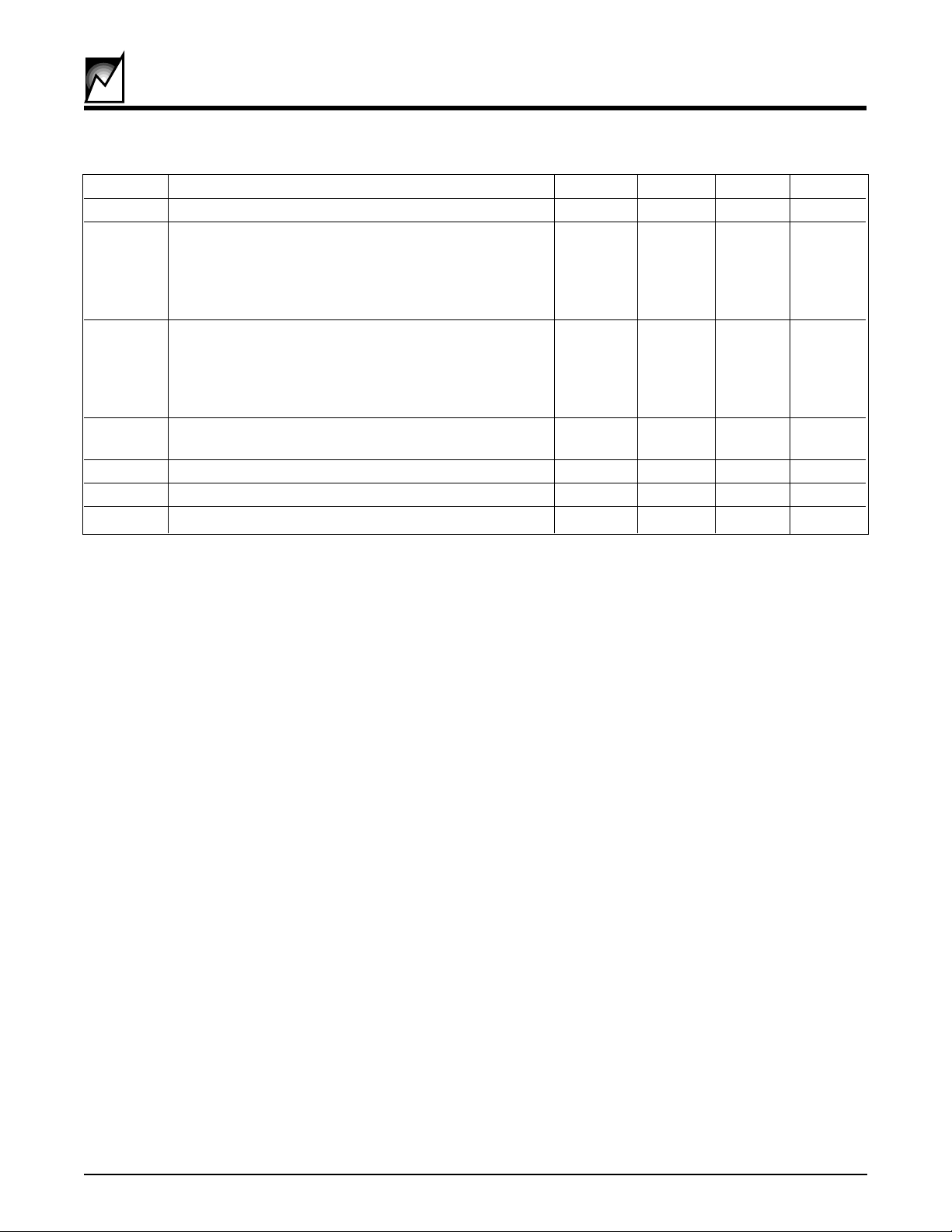
AC Timing Characteristics, -40oC to +85oC
Symbol Description Min. Typ. Max Unit
t
PDD
t
CBD
P
GD
t
FSTSHTDN
t
CYC
t
VGD
t
CBRST
Pin Detect Delay to Vgate enable 80 ms
50mv Circuit Breaker Delay (Filter)
K 400 µs
L 150 µs
M50µs
N5µs
Power Good Delay (PG1/PG2, PG2/PG3)
A5ms
B20ms
C80ms
D 180 ms
Fast Shut Down Delay From Fault to 200 ns
Vgate Off
Circuit Breaker Cycle Mode Cycle Time 2.5 Sec.
Delay from Release of Reset to Vgate on 100 ns
CBReset# Pulse Width 200 ns
2041 8.4 6/15/00
4
SUMMIT MICROELECTRONICS
Page 5
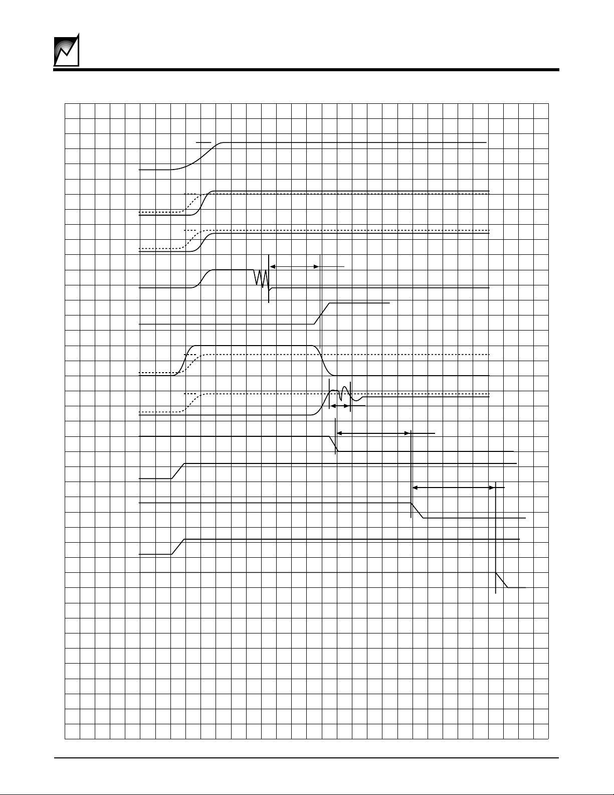
VDD
UV
OV
PD1#/PD2#
Vgate
Drain
Sense
SMH4803
≥11V≤13V
2.5V ref
2.5V ref
tPDD
2.5V ref
CBSense
PG1#
ENPGA
PG2#
ENPGB
PG3#
50mV ref
<tCBD
PGD
PGD
2041 ILL18.0
SUMMIT MICROELECTRONICS
Figure 1. Power Sequencing Timing Characteristics
5
2041 8.4 6/15/00
Page 6
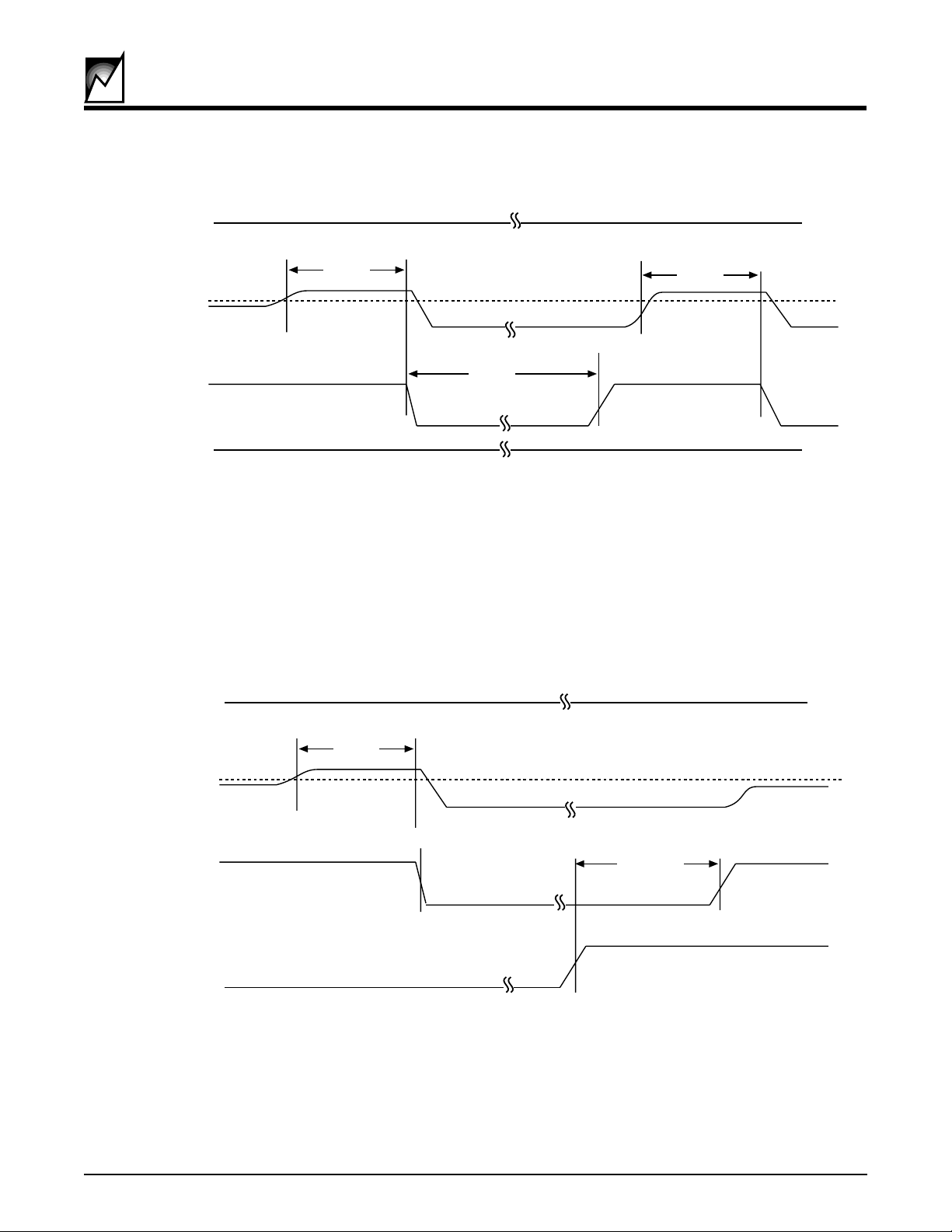
SMH4803
V
IH
CBMode
50mV
CBSense
Vgate
CBReset#
t
CBD
t
CYC
V
IH
Figure 2. Circuit Breaker Timing - Cycle Mode, CBReset# Held High
V
IH
t
CBD
2041 ILL16.0
CBMode
CBSense
Vgate
CBReset#
50mV
V
IL
t
CBD
t
CYC
Figure 3. Circuit Breaker Timing - Cycle Mode, Used to Enable Vgate
2041 ILL17.0
2041 8.4 6/15/00
6
SUMMIT MICROELECTRONICS
Page 7

SMH4803
CBMode
CBSense
Vgate
CBReset#
VIL
tCBD
50mV
tVGD
tCBRST
2041 ILL14.0
Figure 4. Circuit Breaker Timing - Reset Mode
QCB
50mV
CBSense
Vgate
<t
V
Figure 5. Circuit Breaker Timing - Quick-Trip
CBD
t
FSTSHTDN
2041 ILL15.0
SUMMIT MICROELECTRONICS
7
2041 8.4 6/15/00
Page 8

SMH4803
SMH4803 Pin Descripiton
PIN NAME (Pin #)
Drain Sense (1)
The Drain Sense input monitors the voltage at the drain of
the external power MOSFET switch with respect to V
SS
When the MOSFET is turned on, the Drain Sense input
will be driven low and will be used as one of the enable
conditions for the PG outputs. This will prevent any
premature activation of the PG outputs.
Vgate (2)
The Vgate output activates an external power MOSFET
switch. It is a constant current source (100µA typical)
allowing easy programming of the MOSFET turn on slew
rate.
EN/TS (3)
The Enable/Temperature Sense input is the master enable input. When EN/TS is LOW, Vgate, and the PG
outputs are off. As the name suggests, the EN/TS input
may be used as a master enable by a host system or
alternatively for circuit over-temperature protection using
an external thermistor.
PD1# and PD2# (4 & 5)
The pin detect pins are active LOW inputs that are use to
prevent any power sequence before the add-in card is
properly seated. Both inputs must be at VSS before either
Vgate or the PG outputs can be enabled.
In applications where multi-length connector pins are use,
the PD inputs should be tied to the short pins. On the
mating connector side the pins opposite should be tied
directly to VSS. Alternatively, either one or both of the PD
inputs can be tied to card injector handle switches, insuring no power sequencing will occur until the card is
properly seated.
When CBMode is tied to 5V the circuit breaker will be
placed in the self-restart or cycling mode. The state of
CBReset# input will control the operation of the restart. If
CBReset# is tied to 5V the Vgate output will automatically
restart after t
.
exists, the circuit breaker will trip once again. The cycling
has elapsed. If the fault condition still
CYC
will continue until the fault clears or the circuit board is
replaced. Alternatively the CBReset# input can be actively driven to VSS. If a fault occurs the Vgate and PG
outputs will not be turned on again for t
after the
CYC
CBReset# input is driven high.
CBSense (9)
The circuit breaker sense input is used to detect
overcurrent conditions in the load connected to the power
MOSFET. A low value sense resistor (RS) is tied in series
with the MOSFET switch; one end tied to VSS and the
other to the switch and the CBSense input. A voltage drop
of greater than 50mV (for greater than t
) across the
CBD
resistor will result in the circuit breaker tripping. A programmable “quick-trip” sense point is also available. If the
CBSense input transitions above the threshold, the circuit
breaker will immediately trip.
VSS (10)
VSS is connected to the negative side of the supply.
UV and OV (11 & 12)
The under-voltage (11) and over-voltage (12) input pins
monitor the supply voltage for the SMH4803 and the
downstream circuits. Both inputs have a 2.5V threshold
on their respective comparators. If UV is less than 2.5V or
if OV is greater than 2.5V, Vgate will be disabled.
5.0V (13)
5.0V is a precision 5 volt output reference voltage tha may
be use to expand the logic-input funtions on the
SMH4803. The reference output is with respect to VSS.
CBFault# (6)
CBFault# is an open drain active low output, indicating the
circuit breaker status. When an over current condition is
detected CBFault# is driven low.
CBReset# (7)
CBReset# is the circuit breaker reset input. It can be
actively controlled to reset a fault condition or it can be tied
high or low to allow either timed restarts (duty cycle mode)
or “latch-off” the Vgate output. Refer to the Circuit Breaker
Operation and the associated timing diagrams for detailed characteristics.
CBMode (8)
The CBMode input selects one of two circuit breaker
operational modes. When tied to VSS all fault conditions
must be cleared by toggling the CBReset# input low then
high.
2041 8.4 6/15/00
2.5V (14)
2.5V is a precision 2.5 volt output reference voltage tha
may be use to expand the logic-input funtions on the
SMH4803. The reference output is with respect to VSS.
ENPGB (15)
The ENPGB input may be used to independently switch
off the PG3# output. When ENPGB is pulled low, the
PG3# output is immediately placed in a high impedance
state. If PG2# is active and ENPGB is driven high, then
the PG3# output will immediately be driven low.
8
SUMMIT MICROELECTRONICS
Page 9

SMH4803
ENPGA (16)
The ENPGA input controls the PG2# and PG3# outputs.
When ENPGA is pulled low, the PG2# output is immediately placed in a high impedance state. If ENPGA is driven
high, then the PG2# output will immediately be driven low,
provided PG1# has been active for at least t
PGD
.
PG3# (17)
PG3# is an open drain active low output with no internal
pull-up. PG3# is the last power good signal to be enabled
after Vgate, PG1# and PG2# have been turned on. PG3#
is delayed PGD after PG2# is active and 2xPGD after
PG1# is active. PG3# can be used to switch a third load
or a DC/DC converter.
PG1# (18)
PG1# is an open drain active low output with no internal
pull-up. PG1# is enabled after Vgate is enabled and
voltage across the load is within spec. PG1# can be used
to switch a load or enable a DC/DC converter.
PG2# (19)
PG2# is an open drain active low output with no internal
pull-up. PG2# is enabled after Vgate and PG1# have been
turned on. PG2# is delayed PGD after PG1# is active.
PG2# can be used to switch a second load or a DC/DC
converter.
test all combinations (all 128 possibilities) are readily
available as off the shelf stock items.
Power Good Delay
The PG delay timer that controls the delay from PG1# to
PG2# and PG2# to PG3# being asserted can be set to
typical values of 5ms, 20ms, 80ms or 160ms.
Quick-Trip Circuit Breaker Threshold
The Quick-Trip circuit breaker threshold can be set to
200mV, 100mV, 60mv or OFF. This is the threshold
voltage drop across RS that is placed between VSS and
CBSense.
Circuit Breaker Delay
The circuit breaker delay defines the period of time the
voltage drop across RS is greater than 50mV but less than
V
before the Vgate output will be shut down. This is
QCB
effectively a filter to prevent spurious shutdowns of Vgate.
The delays that can be programmed are 5µs, 50µs, 150µs
and 400µs.
Pin Detect
The Pin Detect function can be enabled or disabled.
VDD (20)
VDD is the positive supply connection. An internal shunt
regulator connected between VDD and VSS develops
approximately 12 volts that supplies the SMH4803. A
resistor must be placed in series with the VDD pin to limit
the regulator current (RD in the application illustrations).
PROGRAMMABLE FEATURES
Because the SMH4803 is electrically programmable it
can be fine-tuned for a wide variety of applications prior to
shipment to the customer. Because of this a manufacturer
can use a common part type across a wide range of
boards that are used on a common host but have different
electrical loads, power-on timing requirements, host voltage monitoring needs etc.
This ability to use a common solution across many platforms shifts the focus of design away from designing a
new power interface for each board to concentrating on
the value added back-end logic.
Because the programming of the features is done at final
SUMMIT MICROELECTRONICS
9
2041 8.4 6/15/00
Page 10

SMH4803
DEVICE OPERATION
Power-Up Sequence
The SMH4803 is an integrated power controller for hot
swappable add-in cards. The device operates from a
single supply ranging from 20V to 500V and generates the
signals necessary to drive isolated output DC/DC converters.
The SMH4803 hot-swap controller provides under-voltage and over-voltage monitoring of the host power supply, it drives an external power MOSFET switch that
connects the supply to the load. It also protects against
over-current conditions that might disrupt the host supply.
When the input and output voltages to the SMH4803
controller are within specification, the SMH4803 provides
three “Power Good” logic outputs that may be used to turn
ON loads or drive an LED status light. The SMH4803
provides three separate “Power Good” logic outputs that
activate loads in a programmable timed sequence. There
is a master enable/temperature sense input and 2.5V and
5V reference outputs for expanding monitor functions.
There are two “Power Good” enable inputs that may be
used to activate or deactivate output loads, and dutycycle or reset over-current protection modes to provide
automatic or manual restart of the controller after overcurrent load conditions.
Insertion Process
As the add-in board is inserted into the backplane, physical connections must be made with the chassis to discharge any electrostatic voltage potentials. The board
then contacts the long pins on the backplane that provide
power and ground. As soon as power is applied the
SMH4803 starts up but does not immediately apply power
to the output load. Under-voltage and over-voltage circuits inside the controller check to see if the input voltage
is within a user-specified range, and pin detection signals
determine whether the card is seated properly.
t
after these requirements are met, the hot-swap
PDD
controller enables Vgate to turn on the power MOSFET
switch. The Vgate output is current limited to I
VGATE
allowing the slew rate to be easily modified using external
passive components. During the controlled turn-on period, the Vds of the MOSFET is monitored by the drain
sense input. When Vds drops below a user-specified
voltage the power output is considered to be ON. The
resistor and diode in series with the drain sense input
determine Vds(ON).
Provided there is no sustained over-current condition
during start-up, the SMH4803 turns on the loads with the
Power Good logic outputs. Three DC/DC converters can
be connected to the outputs and their turn-on is
sequenced by pre-programmed delays. If a sustained
over-current condition occurs during or after the insertion
process, then Vgate is shorted to Vss and the MOSFET
switch is turned off to protect the host supply.
Circuit Breaker Operation
The SMH4803 provides a circuit breaker function to
protect against over current conditions. A sustained overcurrent event could damage the host supply and/or the
load circuitry. The board’s load current passes through a
series resistor connected between MOSFET source/
CBSense and Vss on the controller. The breaker will trip
whenever the voltage drop across the series resistor is
greater than 50mV for more than t
instantaneously if the voltage drop exceeds V
, and will trip
CBD
QCB
When the breaker trips, the Vgate output is turned off and
CBFault# will be driven LO. The circuit breaker can be
reset by taking CBReset# LO and then back HI when the
circuit breaker is in the reset mode. In the duty-cycle
mode, the circuit breaker resets automatically after a fixed
time period. If the over current condition still exists after
reset, the circuit will re-trip. In both operating modes of the
circuit breaker, the MOSFET can be switched off by
holding the CBReset input LO.
The value of the over-current shunt resistor is determined
by the following formula: Rs = 50mV/Ioc where Rs is the
value of the shunt resistor and Ioc is the over current limit
determined by the board’s power requirement or the limit
of the host supply.
Current Sense Resistors
Current sense resistors are available from a number of
sources and come in two basic formats: open air sense
resistors and current sense resistor chips. The open air
resistors are metal strips that are available as both thru-hole
and surface mount. The resistor chips are surface mount
and offer excellent thermal characteristics. Both styles are
available in resistance ranges from 3 milliohm to 1 ohm.
IRC (www.irctt.com) is one source for these resistors. The
open air sense resistors can be found in their OARS series,
and the chip resistors are found in their LRC series.
,
Load Control
The SMH4803 is designed to control three or more DC/
DC converters, or other loads, which incorporate ON/OFF
control. The Power Good outputs activate the loads when
the following conditions have been met: the input voltage
to the SMH4803 monitored by UV and OV is within userdefined limits and the external MOSFET is switched ON.
The SMH4803 has three Power Good enable outputs,
PG1#, PG2#, and PG3#, that turn on the DC/DC converter loads in sequence. Output PG1# is activated first,
followed by PG2# after a delay of PGD, and finally PG3#
.
2041 8.4 6/15/00
10
SUMMIT MICROELECTRONICS
Page 11

SMH4803
after another delay PGD. The delays built into the
SMH4803 allow correct sequencing of power to the loads,
e.g. +3V supply must come up before +5V supply. The
delay times are factory programmed. PG2# and PG3#
can be disabled using the ENPGA and ENPGB inputs.
When these inputs are low they override the enable
function produced when the SMH4803 sees a power
good condition.
The PG1#, PG2#, and PG3# outputs have a 12V withstand capability so high voltages must not be connected
to these pins. Inexpensive bipolar transistors will boost
the withstand voltage to that of the host supply, see figure
5 for connections.
Output Slew-Rate Control
The SMH4803 provides a current limited Vgate turn-on.
A fast turn-off is performed by internally shorting Vgate to
Vss. Changing the passive components around the
power MOSFET switch will modify the turn-on slew-rate.
Operating at High Voltages
The breakdown voltage of the external active and passive
components limits the maximum operating voltage of the
SMH4803 hot-swap controller. Components that must be
able to withstand the full supply voltage are: the input and
output decoupling capacitors, the protection diode in
series with DrainSense pin, the power MOSFET switch
and capacitor connected between its drain and gate, the
high-voltage transistors connected to the power good
outputs, and the dropper resistor connected to the
controller’s Vdd pin.
Over-Voltage and Under-Voltage Resistors
In the following examples, the three resistors, R1, R2, and
R3, connected to the OV and UV inputs must be capable
of withstanding the maximum supply voltage which can
be several hundred volts. The trip voltage of the UV and
OV inputs is +2.5V relative to Vss. As the input resistances of UV and OV are very high, high value resistors
can be used in the resistive divider. The divider resistors
should be high stability, 1% metal-film resistors to keep
the under-voltage and over-voltage trip points accurate.
Telecom Design Example
A hot-swap telecom application uses a 48V power supply
with a –25% to +50% tolerance, i.e. the 48V supply can
vary from 36V to 72V. The formulae for calculating R1, R2,
and R3 are shown below.
R1 is calculated from:
Vov
R
1 =
ID
max
VOV is the over-voltage trip point, i.e. 2.5V, therefore:
2.5
min
V
250
µA
Vuv
ID
V
µA
Vuv
min
ID
250
max x
VS
µA
72
)
VS
max
x 36
V
min
V
µA
R
1 = =10kΩ
2) The minimum current that flows through the resistive
divider, IDmin, is easily calculated from the ratio of
maximum and minimum supply voltages:
ID
min =
Therefore:
ID
min = = 125
3) The value of R3 is now calculated using IDmin.
(VS min –
R
3 =
Where Vuv is the under-voltage trip point, also 2.5V,
therefore:
R
3 = = 268kΩ
The closest standard 1% resistor value is 267kΩ
4) R2 may be calculated using:
(R
1 + R2) =
R
2 = –R1
Or
R
2 = –10kΩ = (20kΩ – 10kΩ) = 10kΩ
ID
(36V – 2.5V)
125
Vuv
ID
min
2.5
125µA
1) First select the peak current, IDmax, allowed through
the resistive divider, say 250µA. The value of current
is arbitrary; however, if the current is too high, selfheating in R3 may become a problem (especially in
high voltage systems), and if the current is too low the
value of R3 becomes very large and may be expensive
at 1% tolerance.
SUMMIT MICROELECTRONICS
11
2041 8.4 6/15/00
Page 12

SMH4803
Dropper Resistor Selection
The SMH4803 is powered from the high-voltage supply
via a dropper resistor, Rd. The dropper resistor must
provide the SMH4803 (and its loads) with sufficient operating current under minimum supply voltage conditions,
but must not allow the maximum supply current to be
exceeded under maximum supply voltage conditions.
The dropper resistor value is calculated from:
(
VS
min –
VDD
RD
=
(
IDD
+ I
load
max)
)
Where Vsmin is the lowest operating supply voltage,
Vddmax is the upper limit of the SMH4803 supply voltage,
Idd is minimum current required for the SMH4803 to
operate, and Iload is any additional load current from the
2.5V and 5V outputs and between Vdd and Vss.
The min/max current limits are easily met using the
dropper resistor except in circumstances where the input
voltage may swing over a very wide range, e.g. input
varies between 20V and 100V. In these circumstances it
may be necessary to add an 11V zener diode between
V
and VSS to handle the wide current range. The zener
DD
voltage should be below the nominal regulation voltage of
the SMH4803 so that it becomes the primary regulator.
MOSFET VDS(ON) Threshold
The drain sense input on the SMH4803 monitors the
voltage at the drain of the external power MOSFET switch
with respect to VSS. When the MOSFET’s VDS is below the
user-defined value the switch is considered to be ON. The
VDS(ON) is adjusted using the resistor, RT, in series with
the drain sense protection diode.
This protection or
blocking diode prevents high voltage breakdown of
the drain sense input when the MOSFET switch is
OFF
. An inexpensive 1N4148 diode offers protection up
to 100V. The VDS(ON) threshold is calculated from:
APPLICATIONS CIRCUITS
Reversing Polarity of the Power Good Outputs
The open-drain Power Good outputs on the SMH4803 are
active LO. The output polarity may be changed to active
HI, when required, with a minor circuit change around the
high-voltage buffer transistor, see Figure 6. The 1N4148
blocking diode must be included to prevent high-voltage
damage to the SMH4803.
Expanding Enable/Monitoring on the SMH4803
The 2.5V reference and 5V outputs on the SMH4803
make it easy to expand the number of enable or monitoring inputs. The circuit in Figure 8 illustrates how a quad
low-voltage comparator expands the EN/TS input to four
enable inputs. The comparators draw power from the 5V
output on the SMH4803 and use the 2.5V reference for
the switching threshold. EN1 to EN4 inputs can accept
either analog or CMOS logic level signals between Vss
and +5V. The comparator outputs are ANDed together
and drive the EN/TS input. A 1MΩ resistor adds hysteresis
around the comparators to prevent oscillation near the trip
point.
VDS = V
Where V
– (
I
× R
) –
V
– (
SENSE
DIODE
SENSE
T
DIODE
is the forward voltage drop of the protection
IRS × R
)
S
diode, and IRS is the current flowing through the circuit
breaker sense resistor RS. The VDS(ON) threshold varies
over temperature due to the temperature dependence of
V
DIODE
and I
. The calculation below gives the
SENSE
VDS(ON) threshold under the worst case condition of
+85°C ambient. Using a 68kΩ resistor for RT gives:
VDS(ON) threshold =
2.5V – (15µA x 68kΩ) – V
DIODE
=
2.5 – 1.0 – 0.5 = 1.0V
2041 8.4 6/15/00
12
SUMMIT MICROELECTRONICS
Page 13

SMH4803
0V
PG3#
MMBTA06LT1
SS
V
PG2#
100kΩ
100kΩ
15V
100nF
PG1
PG3#
2.5V 5V
47kΩ
PG2#
OUT
–48V
1N4148
PG1#
Drain
Sense
100nF
+
Rt
68kΩ
Vgate
100V
1kΩ
100µF
100V
*
100 nF
1N4148
10 nF
10Ω
2041 Was5.6
100 V
DS
G
0V
Rd = 10kΩ
R3
SMH4803
Vdd
SS
EN/TS
ENPGB
+12V Wrt V
ENPGB
EN/TS
PD1#
Figure 6. Changing Polarity of Power Good Output PG1#
ENPGA
ENPGA
UV
10kΩ
PD1#
10kΩ
R2
PD2#
OV
CBFault#
CBFault#
CBMode
CBMode
CBSense
Vss
CBReset#
PD2#
100nF
R1
Rs
20mΩ
* 10 ohm resistor must be located as close as possible to the MOSFET.
25V
–48V
SUMMIT MICROELECTRONICS
13
2041 8.4 6/15/00
Page 14

SMH4803
0V
OUT
PG3#
MMBTA06LT1
SS
V
PG2#
100kΩ
100kΩ
15V
100nF
PG1#
PG3#
2.5V 5V
Vdd
100kΩ
PG2#
–48V
Drain
PG1#
Sense
SMH4803
100nF
100V
+
Rt
68kΩ
Vgate
CBSense
2041 Was6.6
100µF
100V
1N4148
10nF
100V
1kΩ
*
10Ω
100nF
* 10 ohm resistor must be located as close as possible to the MOSFET.
Rs
20mΩ
Rd = 10kΩ
SS
+5V Wrt V
SS
SS
+12V Wrt V
+2.5V Wrt V
R3
PD1#
1k
1M
EN/TS
ENPGB
ENPGB
LMV331
ENPGA
ENPGA
UV
10kΩ
PD1#
10kΩ
R2
PD2#
OV
CBFault#
CBFault#
CBMode
CBMode
Vss
CBReset#
PD2#
100nF
25V
R1
2041 8.4 6/15/00
0V
NTC
50k
MAX
@T
Figure 7. Overtemperature Shutdown on SMH4803
50k
14
–48V
SUMMIT MICROELECTRONICS
Page 15

0V
OUT
PG3#
MMBTA06LT1
SS
V
100kΩ
100kΩ
PG2#
100nF
15V
PG1#
PG3#
2.5V 5V
Vdd
100kΩ
PG2#
–48V
Drain
PG1#
Sense
SMH4803
100nF
100V
+
Rt
68kΩ
1kΩ
Vgate
CBSense
100µF
100V
*
100nF
1N4148
10nF
10Ω
SMH4803
2041 Was7.5
100V
* 10 ohm resistor must be located as close as possible to the MOSFET.
Rs
20mΩ
Rd = 10kΩ
SS
+5V Wrt V
SS
+2.5V Wrt V
R3
1kΩ
10kΩ
EN/TS
PD1#
EN/TS
ENPGB
ENPGA
ENPGB
ENPGA
1MΩ
+
–
UV
10kΩ
PD1#
R2
PD2#
10kΩ
OV
CBFault#
Vss
CBFault#
CBMode
CBMode
–
CBReset#
+
PD2#
100nF
25V
R1
0V
SUMMIT MICROELECTRONICS
+
–
LMV339
EN1
EN2
EN3
Figure 8. Expanding Input Monitoring Capability
15
–
EN4
+
–48V
2041 8.4 6/15/00
Page 16

V3
SMH4803
ISOLATED
DC
OUTPUTS
V1
V2
+
–48V
Isolated
0V
#2
DC/DC
–48V
#1
DC/DC
Isolated
2041 Was12.3
–48V
Isolated
Rd = 10kΩ
R3
#3
DC/DC
+12V
100kΩ
ENPGA
ENPGB
Vdd
EN/TS
5V
UV
PG3#
PD1#
R2
100kΩ
PG2#
PD2#
10kΩ
CBSense
OV
SMH4803
3x MMBTA06LT1
100kΩ
Drain Sense
PG1#
*
10Ω
Vgate
Vss
R1
* 10Ω resistor must be located as close as possible to the MOSFET.
Rs
2041 8.4 6/15/00
0V
10kΩ
25V
100nF
PD1#
Figure 9. Typical Application Sequencing 3 DC/DC Converters
EN/TS
16
PD2#
–48V
SUMMIT MICROELECTRONICS
Page 17

V3
ISOLATED
DC
V2
V1
SMH4803
OUTPUTS
+
0V
2041 IWas9.5
+5V
RESET
RESET
RESET1#
RESET2#
V1
–48V
–48V
#1
DC/DC
Isolated
#2
DC/DC
Isolated
–48V
#3
DC/DC
Isolated
Drain Sense
5V
Rd
+12V
ENPGA
ENPGB
Vdd
EN/TS
UV
PG3#
PD1#
PG2#
PD2#
CBSense
OV
SMH4803
PG1#
Vgate
Vss
R1
Ω
*
10
* 10Ω resistor must be located as close as possible to the MOSFET.
Rs
+
R3
R2
10kΩ
SUMMIT MICROELECTRONICS
100nF
25V
10kΩ
0V
PD1#
Figure 10. Sequencing 3 DC/DC Converters with Output Voltage Feedback
17
EN/TS
PD2#
–48V
2041 8.4 6/15/00
Page 18

SMH4803
V3
V2
RESET
V1
RESET
RESET1#
OV
+
2041 Was11.3
–48V
–48V
#1
DC/DC
Isolated
#2
DC/DC
Isolated
–48V
#3
DC/DC
Isolated
RESET2#
2x1N4148
2x
MMBTA56LT1
47 K 47 K
OV
47 K
47 K
R3
Rd
PD1#
10 K
EN/TS
ENPGA
ENPGB
Vdd
5V
UV
PG3#
PD1#
R2
PG2#
PD2#
25V
100nF
CBSense
OV
PD2#
SMH4803
PG1#
Vgate
Vss
R1
10 K
Drain
*
10
Sense
* 10 ohm resistor must be located as close as possible to the MOSFET.
Rs
–48V
2041 8.4 6/15/00
Figure 11. Sequencing Converters with Common I/O Ground and Voltage Feedback
18
SUMMIT MICROELECTRONICS
Page 19

20-Lead Small Outline Package (SOIC)
0.291 - 0.299
(7.391 - 7.595)
0.010 - 0.029
(0.254 - 0.737)
x45°
0° to 8°
typ
0.093 - 0.104
(2.362 - 2.642)
SMH4803
0.496 - 0.512
(12.598 - 13.005)
0.394 - 0.419
(10.007 - 10.643)
0.037 - 0.045
(0.940 - 1.143
0.009 - 0.013
(0.229 - 0.330)
0.016 - 0.050
(0.406 - 1.270)
0.050
(1.270)
0.014 - 0.019
(0.356 - 0.482)
0.004 - 0.012
(0.102 - 0.305)
20pn SOIC ILL.1
SUMMIT MICROELECTRONICS
19
2041 8.4 6/15/00
Page 20

ORDERING INFORMATION
SMH4803
Base Part Number
Power Good Delay
A = 5ms
B = 20ms
C = 80ms
D = 160ms
SMH4803
AEKP
Pin Detect Function
Blank = Enabled
P = Disabled
Circuit Breaker Delay
K = 400µs
L = 150µs
M = 50µs
N = 5µs
Quick-T rip Threshold
E = 200mV
F = 100mV
H = 60mV
J = OFF
2041 ILL8.3
2041 8.4 6/15/00
20
SUMMIT MICROELECTRONICS
Page 21

SMH4803
Valid Part Number Combinations
SMH4803 A E K SMH4803 C E K
SMH4803 A E L SMH4803 C E L
SMH4803 A E M SMH4803 C E M
SMH4803 A E N SMH4803 C E N
SMH4803 AEKP SMH4803 C E K P
SMH4803 A E L P SMH4803 C E L P
SMH4803 A E M P SMH4803 C E M P
SMH4803 A E N P SMH4803 C E N P
SMH4803 A F K SMH4803 C F K
SMH4803 A F L SMH4803 C F L
SMH4803 A F M SMH4803 C F M
SMH4803 A F N SMH4803 C F N
SMH4803 A F K P SMH4803 C F K P
SMH4803 A F L P SMH4803 C F L P
SMH4803 A F M P SMH4803 C F M P
SMH4803 A H N P SMH4803 C H N P
SMH4803 A H K SMH4803 C H K
SMH4803 A H L SMH4803 C H L
SMH4803 A H M SMH4803 C H M
SMH4803 A H N SMH4803 C H N
SMH4803 A H K P SMH4803 C H K P
SMH4803 A H L P SMH4803 C H L P
SMH4803 A H M P SMH4803 C H M P
SMH4803 A H N P SMH4803 C H N P
SMH4803 A J K SMH4803 C J K
SMH4803 A J L SMH4803 C J L
SMH4803 A J M SMH4803 C J M
SMH4803 A J N SMH4803 C J N
SMH4803 A J K P SMH4803 C J K P
SMH4803 A J L P SMH4803 C J L P
SMH4803 A J M P SMH4803 C J M P
SMH4803 A J N P SMH4803 C J N P
SMH4803 B E K SMH4803 D E K
SMH4803 B E L SMH4803 D E L
SMH4803 B E M SMH4803 D E M
SMH4803 B E N SMH4803 D E N
SMH4803 BEKP SMH4803 D E K P
SMH4803 B E L P SMH4803 D E L P
SMH4803 B E M P SMH4803 D E M P
SMH4803 B E N P SMH4803 D E N P
SMH4803 B F K SMH4803 D F K
SMH4803 B F L SMH4803 D F L
SMH4803 B F M SMH4803 D F M
SMH4803 B F N SMH4803 D F N
SMH4803 B F K P SMH4803 D F K P
SMH4803 B F L P SMH4803 D F L P
SMH4803 B F M P SMH4803 D F M P
SMH4803 B H N P SMH4803 D H N P
SMH4803 B H K SMH4803 D H K
SMH4803 B H L SMH4803 D H L
SMH4803 B H M SMH4803 D H M
SMH4803 B H N SMH4803 D H N
SMH4803 B H K P SMH4803 D H K P
SMH4803 B H L P SMH4803 D H L P
SMH4803 B H M P SMH4803 D H M P
SMH4803 B H N P SMH4803 D H N P
SMH4803 B J K SMH4803 D J K
SMH4803 B J L SMH4803 D J L
SMH4803 B J M SMH4803 D J M
SMH4803 B J N SMH4803 D J N
SMH4803 B J K P SMH4803 D J K P
SMH4803 B J L P SMH4803 D J L P
SMH4803 B J M P SMH4803 D J M P
SMH4803 B J N P SMH4803 D J N P
SUMMIT MICROELECTRONICS
21
2041 8.4 6/15/00
Page 22

SMH4803
NOTICE
SUMMIT Microelectronics, Inc. reserves the right to make changes to the products contained in this publication in order
to improve design, performance or reliability. SUMMIT Microelectronics, Inc. assumes no responsibility for the use of
any circuits described herein, conveys no license under any patent or other right, and makes no representation that
the circuits are free of patent infringement. Charts and schedules contained herein reflect representative operating
parameters, and may vary depending upon a user’s specific application. While the information in this publication has
been carefully checked, SUMMIT Microelectronics, Inc. shall not be liable for any damages arising as a result of any
error or omission.
SUMMIT Microelectronics, Inc. does not recommend the use of any of its products in life support or aviation applications
where the failure or malfunction of the product can reasonably be expected to cause any failure of either system or to
significantly affect their safety or effectiveness. Products are not authorized for use in such applications unless
SUMMIT Microelectronics, Inc. receives written assurances, to its satisfaction, that: (a) the risk of injury or damage has
been minimized; (b) the user assumes all such risks; and (c) potential liability of SUMMIT Microelectronics, Inc. is
adequately protected under the circumstances.
© Copyright 2000 SUMMIT Microelectronics, Inc.
2041 8.4 6/15/00
22
SUMMIT MICROELECTRONICS
 Loading...