

Page 1
SUMMIT
MICROELECTRONICS, Inc.
SMH4803A
Distributed Power Hot Swap Controller
FEATURES
l Soft Starts Main Power Supply on Card Insertion
or System Power Up
l Senses Card Insertion via Short Pins or Ejector
Switches
l Master Enable to Allow System Control of Power
Up or Down
w Can be used as a Temperature Sense Input
l Programmable Independent Controls of 3 DC/DC
Converters
w Not Enabled until Host Supply Fully Soft
Started
w Programmable Time Delay Between each
Enable Signal
w Available Input to hold off Dependant Enables
until Conditions are Satisfied
l Highly Programmable Circuit Breaker
w Programmable Quick-TripTM Values
w Programmable Current Limiting
Preliminary
w Programmable Circuit Breaker Mode:
Latched (Volatile or Nonvolatile)
w Programmable Duty Cycle Times
w Programmable Over-current Filter
l Programmable Host Voltage Fault Monitoring
w Programmable Under- voltage Hysteresis
w Programmable UV/OV Voltage Filter
w Programmable Fault Mode: Latched or Duty
Cycle
l Nonvolatile Programming to Customize Features
w Available Pre-programmed from Summit
l 2.5V and 5.0V Reference Outputs
w Eliminates the Need or Other Primary Volt-
ages
w Easy Expansion of External Monitor Func-
tions
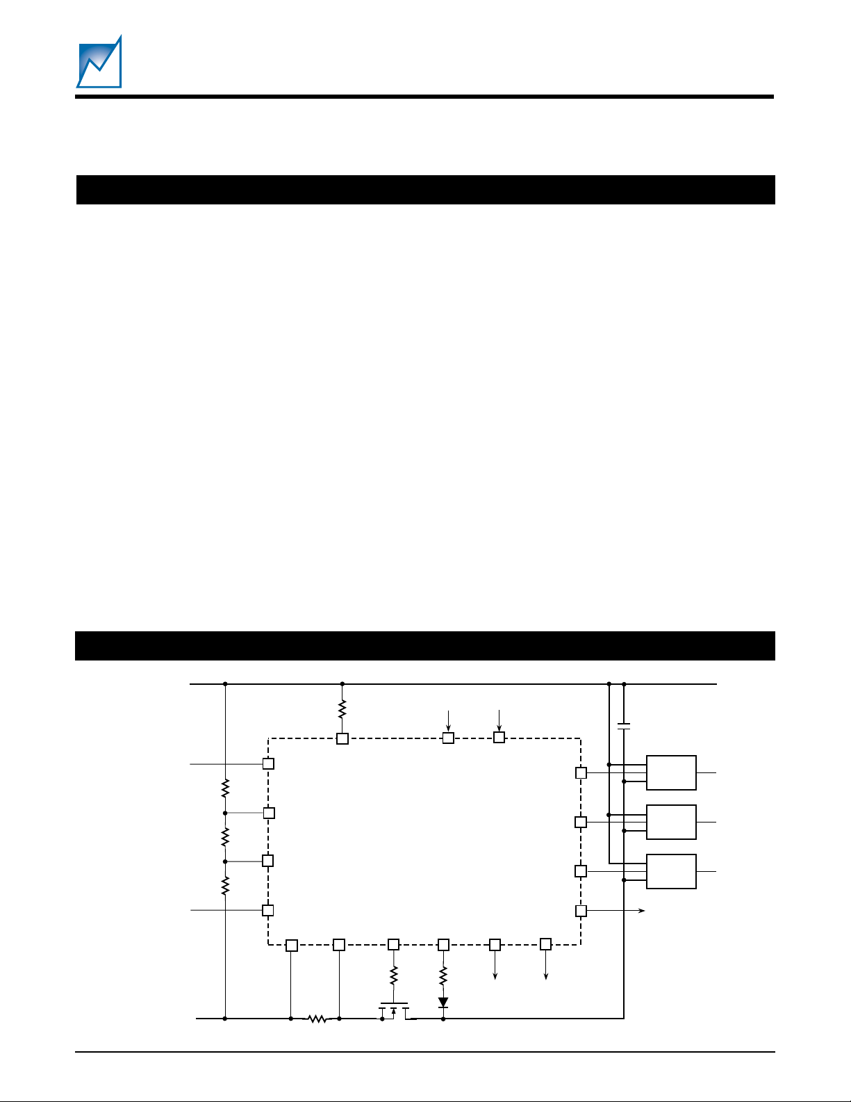
SIMPLIFIED APPLICATION DRAWING
0V
Pin Detect
Pin Detect
PD1#
R3
UV
R2
OV
R1
PD2#
VSS
VDD
CBSENSE
VGATE
l Supply Range ±20VDC to >±500VDC
Disable / Enable
ENPGA
SMH4803A
DRAIN
SENSE
ENPGB
2.5VREF
PG1#
PG2#
PG3#
FAULT#
5.0VREF
DC/DC
DC/DC
DC/DC
–48V
©SUMMIT MICROELECTRONICS, Inc., 2000 • 300 Orchard City Dr., Suite 131 • Campbell, CA 95008 • Phone 408-378-6461 • FAX 408-378-6586 • www.summitmicro.com
Characteristics subject to change without notice
2051 4.4 3/15/01
2051 SAD 1.2
1
Page 2
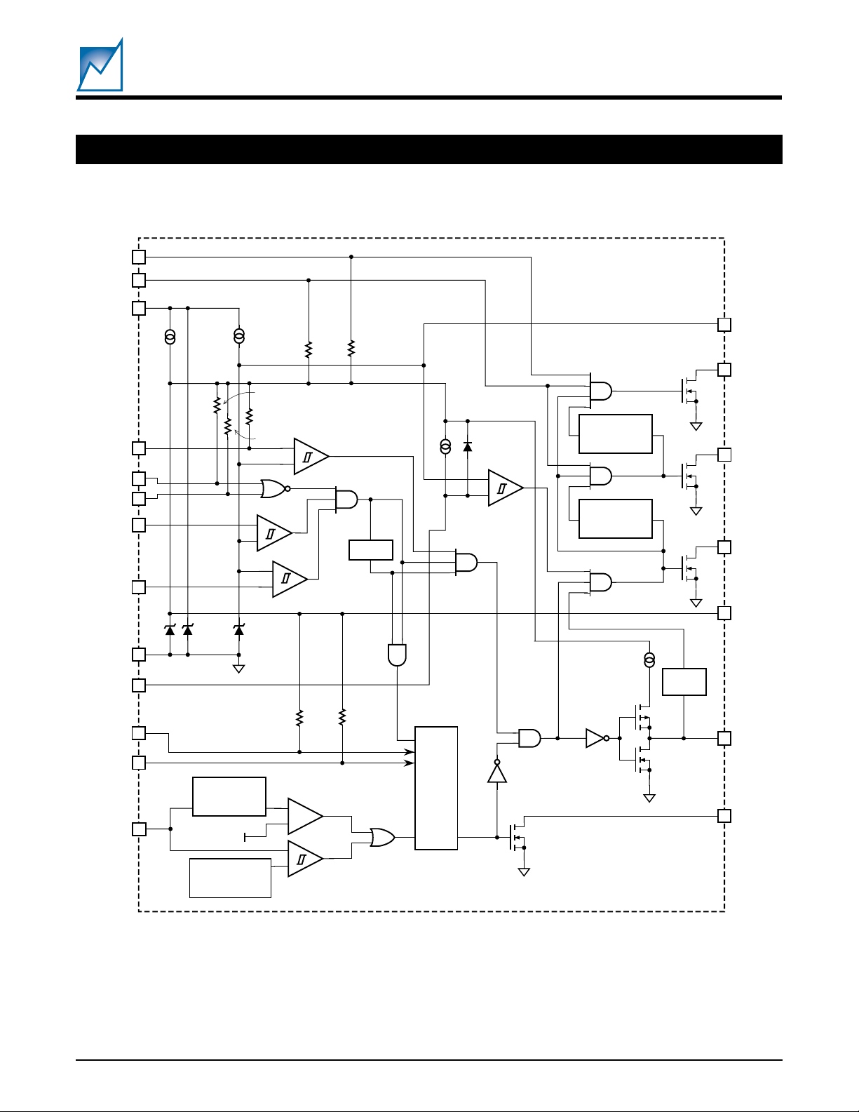
FUNCTIONAL BLOCK DIAGRAM
SMH4803A
Preliminary
ENPGB
ENPGA
VDD
EN/TS
PD1#
PD2#
UV
OV
VSS
DRAIN
SENSE
MODE
15
16
5V
12VREF
12V
2.5V
50kΩ
200kΩ
50kΩ
+
–
14
2.5VREF
50kΩ
+
–
+
–
50kΩ
50kΩ
FILTER
50kΩ
17
PG3#
PROGRAMM-
ABLE
DELAY
+
–
PROGRAMM-
ABLE
DELAY
VGATE
SENSE
19
18
13
2
PG2#
PG1#
VGATE
5.0VREF
20
3
4
5
11
12
10
1
8
RESET#
CBSENSE
2
7
PROGRAMM-
ABLE
DELAY
9
50mV
Programmable
Quick Trip
Ref. Voltage
+
–
+
–
FAULT
LATCH
AND
DUTY
CYCLE
TIMER
2051 4.4 3/15/01
6
FAULT#
2051 BD 1.3
SUMMIT MICROELECTRONICS, Inc.
Page 3
SMH4803A
Preliminary
PRODUCT DESCRIPTION
The SMH4803A is an integrated solution for high reliability
systems to monitor and react to events that could have a
detrimental effect on a system. It can contain or limit faults
to a single circuit board before that fault propagates to the
system. Its programmability lets a single board satisfy
multiple circuit demands while customized to meet special
requirements.
The SMH4803A monitors and controls the primary voltage
in a distributed power system while providing for both hotswapping and secondary voltage sequencing in multisupply systems. The primary power source can be shut
down if events are sensed that could result in damage to
either the circuit board or the system supply. An external
FET switch is used to soft start the primary voltage once
normal operating conditions are met. The external FET
also uses an external shunt to monitor current for the
circuit breaker function.
The SMH4803A sequences secondary voltage by timed
or externally controlled outputs that enable DC/DC converters. Its reference voltages provide isolation between
primary and secondary voltages, but allow expansion of its
features.
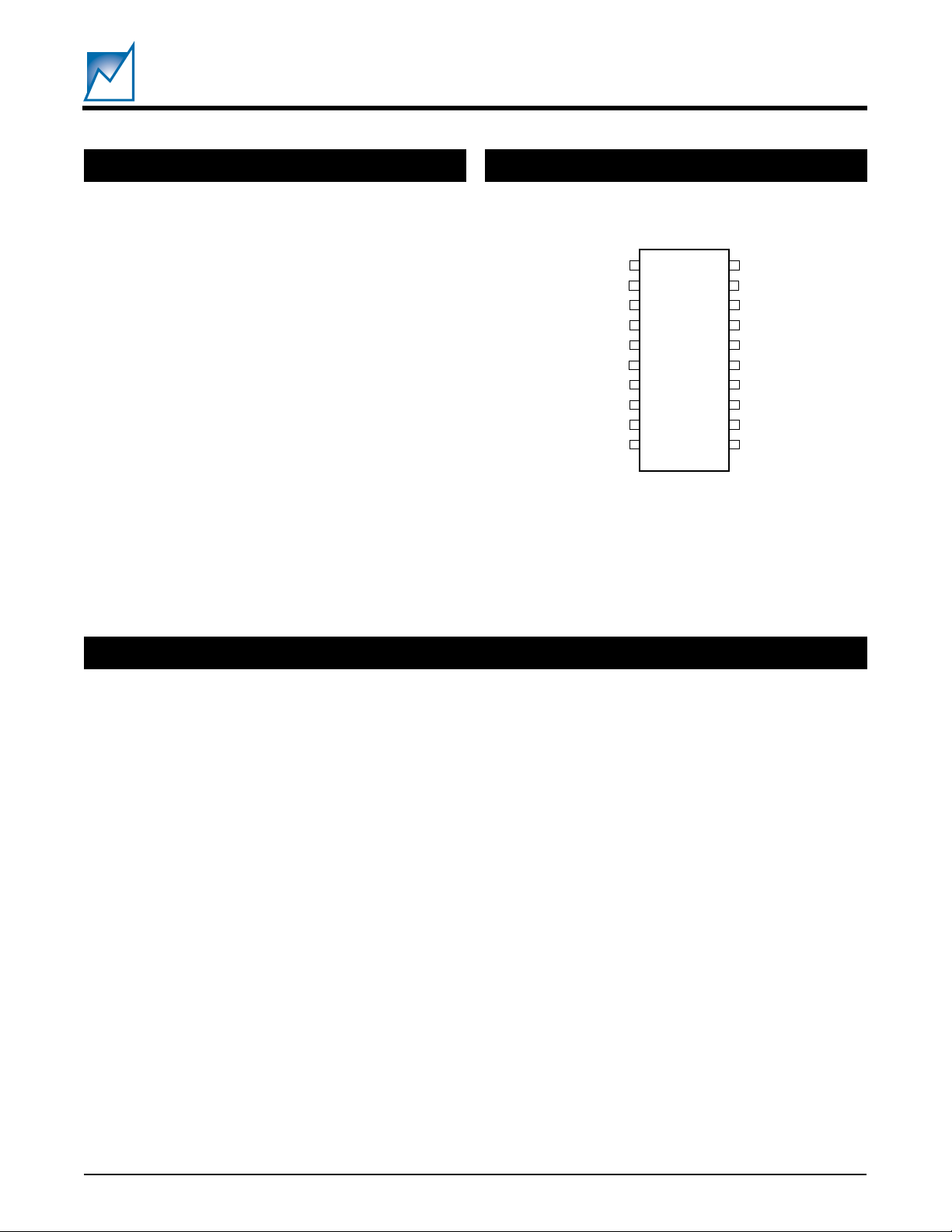
PIN CONFIGURATION
20-Pin SOIC
DRAIN SENSE
VGATE
EN/TS
PD1#
PD2#
FAULT#
RESET#
MODE
CBSENSE
V
SS
1
2
3
4
5
6
7
8
9
10
20
19
18
17
16
15
14
13
12
11
V
DD
PG2#
PG1#
PG3#
ENPGA
ENPGB
2.5VREF
5.0VREF
OV
UV
2051 PCon 1.0
PIN DESCRIPTIONS
DRAIN SENSE (1)
The DRAIN SENSE input monitors the voltage at the drain
of the external power MOSFET switch with respect to VSS.
An internal 10µA source pulls the DRAIN SENSE signal
towards the 5V reference level. DRAIN SENSE must be
held below 2.5V to enable the PG outputs.
VGATE (2)
The VGATE output activates an external power MOSFET
switch. This signal supplies a constant current output
(100µA typical), which allows easy adjustment of the
MOSFET turn on slew rate.
EN/TS (3)
The Enable/Temperature Sense input is the master enable input. If EN/TS is less than 2.5V, VGATE will be
disabled. This pin has an internal 200kΩ pull-up to 5V.
PD1# and PD2# (4 & 5)
These are logic level active low inputs that can optionally
be employed to enable VGATE and the PG outputs when
they are at VSS. These pins each have an internal 50kΩ
pull-up to 5V.
FAULT# (6)
This is an open-drain, active-low output that indicates the
fault status of the device.
RESET# (7)
Reset# is used to clear latched fault conditions. When this
pin is held low the VGATE and PG outputs are disabled.
Refer to the Circuit Breaker Operation and the associated
timing diagrams for detailed characteristics. This pin has
an internal 50kΩ pull-up to 5V.
MODE (8)
The state of the MODE signal determines how fault
conditions are cleared. The device is in the latched mode
when the signal is held at VSS, and the cycle mode when
held at 5V or left floating. This pin has an internal 50kΩ
pull-up to 5V.
CBSENSE (9)
The circuit breaker sense input is used to detect overcurrent conditions across an external, low value sense
resistor (RS) tied in series with the Power MOSFET. A
voltage drop of greater than 50mV across the resistor for
longer than t
will trip the circuit breaker. A program-
CBD
mable Quick-Trip™ sense point is also available.
SUMMIT MICROELECTRONICS, Inc.
2051 4.4 3/15/01
3
Page 4
SMH4803A
Preliminary
UV (11)
The UV pin is used as an under-voltage supply monitor,
typically in conjunction with an external resistor ladder.
VGATE will be disabled if UV is less than 2.5V. Programmable internal hysteresis is available on the UV input,
adjustable in increments of 62.5mV. Also available is a
filter delay on the UV input.
OV (12)
The OV pin is used as an over-voltage supply monitor,
typically in conjunction with an external resistor ladder.
VGATE will be disabled if OV is greater than 2.5V. A filter
delay is available on the OV input.
5.0VREF & 2.5VREF (13 & 14)
These are precision 5V and 2.5V output reference voltages that may be use to expand the logic input functions
on the SMH4803A. The reference outputs are with respect to V
SS
.
ENPGA (16)
This is an active high input that controls the PG2# and
PG3# outputs. When ENPGA is pulled low the PG2# and
PG3# outputs are immediately placed in a high impedance
state. When ENPGA is driven high or left floating then
PG2# will be driven low at a time period of t
after PG1#
PGD
has been active. This pin has an internal 50kΩ pull-up to
5V.
ENPGB (15)
This is an active high input that controls the PG3# output.
When ENPGB is pulled low the PG3# output is immediately placed in a high impedance state. When ENPGB is
driven high or left floating then PG3# will be driven low at
a time period of t
after PG2# has been active. This pin
PGD
has an internal 50kΩ pull-up to 5V.
PG1#, PG2#, & PG3# (18, 19, & 17)
The PGn# pins are open-drain, active-low outputs with no
internal pull-up resistor. They can be used to switch a load
or enable a DC/DC converter. PG1# is enabled immediately after VGATE reaches VDD – VGT and the DRAIN
SENSE voltage is less than 2.5V. Each successive PG
output is enabled t
after its predecessor, provided also
PGD
that the appropriate ENPG input(s) are high. Voltage on
these pins cannot exceed 12V, as referenced to V
SS.
VDD (20)
VDD is the positive supply connection. An internal shunt
regulator limits the voltage on this pin to approximately
12V with respect to VSS. A resistor must be placed in
series with the VDD pin to limit the regulator current (RD in
the application illustrations).
VSS (10)
VSS is connected to the negative side of the supply.
RECOMMENDED OPERATING CONDITIONS
Temperature –40°C to 85°C.
ABSOLUTE MAXIMUM RATINGS*
Temperature Under Bias ...................... –55°C to 125°C
Storage Temperature ........................... –65°C to 150°C
Lead Solder Temperature (10s)........................... 300°C
Terminal Voltage with Respect to VSS:
VGATE ......................................... VDD + 0.5V
UV, OV, CBSENSE, DRAIN SENSE,
FAULT#, PG1#, PG2#,
and PG3# ...................... –0.5V to VDD + 0.5V
4
2051 4.4 3/15/01
PD1#, PD2#, MODE, RESET#,
ENPGA, ENPGB, EN/TS ......................... 10V
*Comment
Stresses listed under Absolute Maximum Ratings may cause permanent damage to the device. These are stress ratings only, and
functional operation of the device at these or any other conditions
outside those listed in the operational sections of this specification is not
implied. Exposure to any absolute maximum rating for extended
periods may affect device performance and reliability.
SUMMIT MICROELECTRONICS, Inc.
Page 5
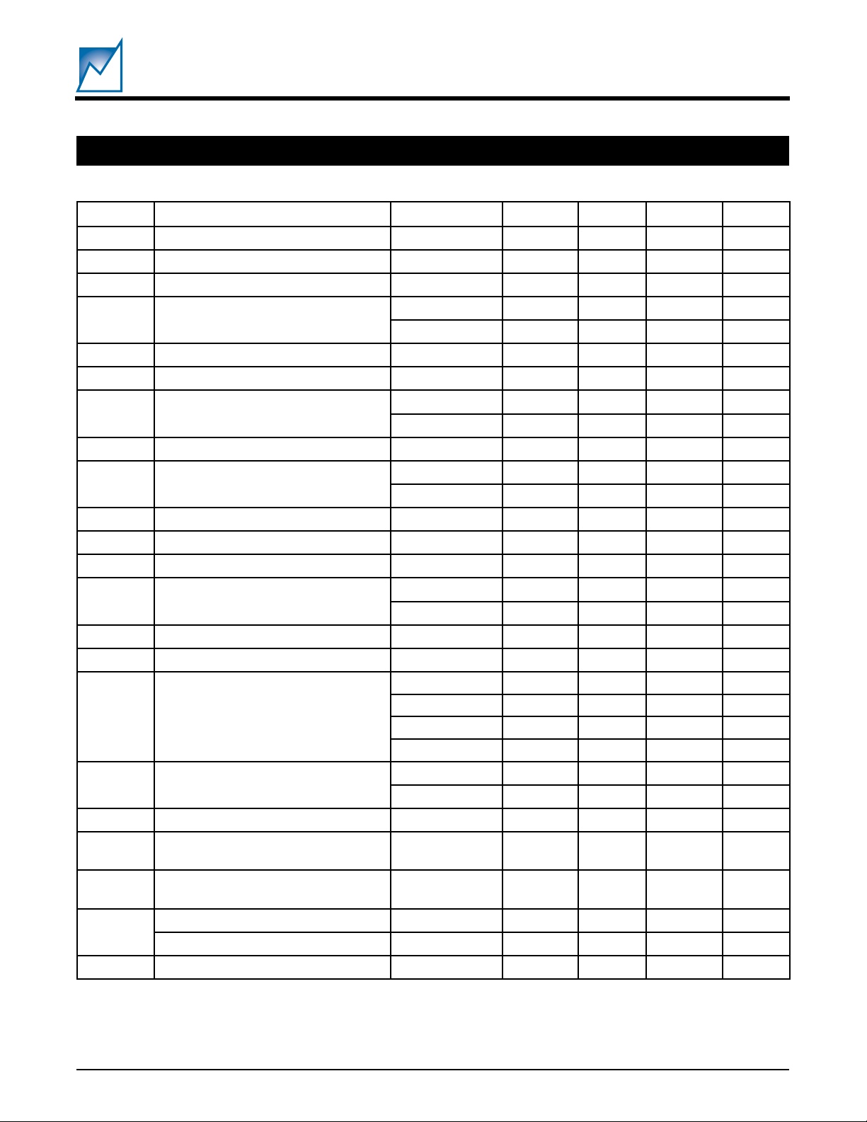
DC OPERATING CHARACTERISTICS
(Over Recommended Operating Conditions; Voltages are relative to VSS, except VGT)
lobmySretemaraPsnoitidnoC.niM.pyT.xaMstinU
V
DD
FERV0.5tuptuoecnereferV5I
I
5DAOL
FERV5.2tuptuoecnereferV5.2
I
5.2DAOL
I
DD
V
VU
V
TSYHVU
V
VO
V
TSYHVO
V
ETAGV
I
ETAGV
V
ESNES
I
ESNES
V
BC
V
BCQ
V
STNE
V
V
V
V
V
(1) TA = 25°C.
TSYHSTNE
HI
LI
LO
TG
egatlovylppuSI
tnerructuptuoecnereferV5I
I
I
tnerructuptuoecnereferV5.2I
tnerrucylppusrewoPdelbanetuptuO2 01Am
I
dlohserhtegatloV-rednU
I
siseretsyhegatloV-rednUI
I
dlohserhtegatloV-revO
I
siseretsyhegatloV-revOI
egatlovtuptuoETAGV V
tuptuotnerrucETAGV001Aµ
I
dlohserhtESNESNIARD
I
tuptuotnerrucESNESNIARDV
dlohserhtrekaerbtiucriCI
tiucricpirTkciuQelbammargorP
dlohserhtrekaerb
I
dlohserhtST/NE
I
siseretsyhST/NEI
,B/AGPNE:egatlovhgihtupnI
#TESER,EDOM
,B/AGPNE:egatlovwoltupnI
#TESER,EDOM
#TLUAF:egatlovwoltuptuOI
#3/#2/#1GP:egatlovwoltuptuOI
dlohserhtetaG7.08.10.3V
Am3=112131V
DD
Am3=57.400.552.5V
DD
Am3=1– 1Am
DD
Am3=)1(574.2005.2525.2V
DD
Am3=524.2005.2575.2V
DD
Am3=2.0– 1Am
DD
Am3=)1(574.2005.2525.2V
DD
Am3=524.2005.2575.2V
DD
Am3=01Vm
DD
Am3=)1(574.2005.2525.2V
DD
Am3=524.2005.2575.2V
DD
Am3=01Vm
DD
Am3=)1(574.2005.2525.2V
DD
Am3=524.2005.2575.2V
DD
V=
ESNES
DD
)1(9 0111Aµ
SS
Am3=040506Vm
002Vm
001Vm
06Vm
ffO —
Am3=)1(574.2005.2525.2V
DD
Am3=524.2005.2575.2V
DD
Am3=01Vm
DD
2FERV0.5V
1.0– 8.0V
Am2=0 4.0V
LO
Am2=0 4.0V
KNIS
SMH4803A
Preliminary
DD
V
2051 Elect Table 2.2
SUMMIT MICROELECTRONICS, Inc.
2051 4.4 3/15/01
5
Page 6

FUNCTIONAL DESCRIPTION
SMH4803A
Preliminary
GENERAL OPERATION
The SMH4803A is an integrated power controller for hot
swappable add-in cards. The device operates from a wide
supply range and generates the signals necessary to drive
isolated output DC/DC converters. As a typical add-in
board is inserted into the powered backplane physical
connections must first be made with the chassis to discharge any electrostatic voltage potentials. The board
then contacts the long pins on the backplane that provide
power and ground. As soon as power is applied the device
starts up, but does not immediately apply power to the
output load. Under-voltage and over-voltage circuits
inside the controller check to see that the input voltage is
within a user-specified range, and pin detection signals
determine whether the card is seated properly.
These requirements must be met for a Pin Detect Delay
period of t
, after which time the hot-swap controller
PDD
enables VGATE to turn on the external power MOSFET
switch. The VGATE output is current limited to I
VGATE
allowing the slew rate to be easily modified using external
passive components. During the controlled turn-on period
the VDS of the MOSFET is monitored by the drain sense
input. When drain sense drops below 2.5V, and VGATE
gets above VDD – VGT, the power good outputs can begin
turning on the DC/DC controllers. Power Good Enable
inputs may be used to activate or deactivate specific
output loads.
Steady state operation is maintained as long as all conditions are normal. Any of the following events may cause
the device to disable the DC/DC controllers by shutting
down the power MOSFET: an under-voltage or overvoltage condition on the host power supply; an overcurrent event detected on the CBSENSE input; a failure of
the power MOSFET sensed via the DRAIN SENSE pin;
the pin detect signals becoming invalid; or the master
enable (EN/TS) falling below 2.5V. The SMH4803A may
be configured so that after any of these events occur the
VGATE output shuts off and either latches into an off state
or recycles power after a cooling down period, t
Powering V
DD
CYC
.
The SMH4803A contains a shunt regulator on the VDD pin
that prevents the voltage from exceeding 12V. It is
necessary to use a dropper resistor (RD) between the host
power supply and the VDD pin in order to limit current into
the device and prevent possible damage. The dropper
resistor allows the device to operate across a wide range
of system supply voltages, and also helps protect the
device against common-mode power surges. Refer to the
Applications Section for help on calculating the RD resistance value.
6
2051 4.4 3/15/01
System Enables
There are several enabling inputs, which allow a host
system to control the SMH4803A. The Pin Detect pins
(PD1# & PD2#) are two active low enables that are
generally used to indicate that the add-in circuit card is
properly seated. This is typically done by clamping the
inputs to VSS through the implementation of an injector
switch, or alternatively through the use of a staggered pins
at the card-cage interface. Two shorter pins arrayed at
opposite ends of the connector force the card to be fully
seated (not canted) before both pin detects are enabled.
Care must be taken not to exceed the maximum voltage
rating of these pins during the insertion process. Refer to
details in the Applications Section for proper circuit implementation.
The EN/TS input provides an active high comparator input
that may be used as a master enable or temperature
sense input. These inputs must be held low for a period of
t
before a power-up sequence may be initiated.
PDD
,
Under-/Over-Voltage Sensing
The Under-Voltage (UV) and Over-Voltage (OV) inputs
provide a set of comparators that act in conjunction with an
external resistive divider ladder to sense when the host
supply voltage exceeds the user defined limits. If the input
to the UV pin rises above 2.5V, or the input to the OV pin
falls below 2.5V for a period of t
quence may be initiated. The t
, the power-up se-
PDD
filter helps prevent
PDD
spurious start-up sequences while the card is being inserted. If UV falls below 2.5V or OV rises above 2.5V, the
PG and VGATE outputs will be shut down immediately.
Under-/Over-Voltage Filtering
The SMH4803A may also be configured so that an out of
tolerance condition on UV/OV will not shut off the output
immediately. Instead, a filter delay may be inserted so that
only sustained under-voltage or over-voltage conditions
will shut off the output. When the UV/OV filter option is
enabled an out of tolerance condition on UV/OV for longer
than the filter delay time, t
, activates the FAULT#
UOFLTR
output, and the VGATE and PG outputs will be latched in
the off state. To initiate another power-up sequence the
FAULT# output must first be reset. Refer to the appropriate section on resetting the FAULT# output. The Under/Over-Voltage Filtering feature is disabled in the default
configuration of the device.
Under-Voltage Hysteresis
The Under-Voltage comparator input may be configured
with a programmable level of hysteresis. The compare
SUMMIT MICROELECTRONICS, Inc.
Page 7

SMH4803A
Preliminary
level may be set in steps (up to 15) of 62.5mV below 2.5V.
The default under-voltage hysteresis level is set to
62.5mV.
Soft Start Slew Rate Control
Once all of the preconditions for powering up the DC/DC
controllers have been met, the SMH4803A provides a
means to soft start the external power FET. It is important
to limit in-rush current to prevent damage to the add-in
card or disruptions to the host power supply. For example,
charging the filter capacitance (normally required at the
input of the DC/DC controllers) too quickly may generate
very high current. The VGATE output of the SMH4803A
is current limited to I
, allowing the slew rate to be
VGATE
easily modified using external passive components. The
slew rate may be found by dividing I
by the gate-to-
VGATE
drain capacitance placed on the external FET. A complete
design example is given in the Applications Section.
Load Control — Sequencing the Secondary Supplies
Once power has been ramped to the DC/DC controllers,
two conditions must be met before the PGn# outputs can
be enabled: the Drain Sense voltage must be below 2.5V,
and the VGATE voltage must be greater than VDD –VGT.
The Drain Sense input helps ensure that the power MOSFET is not absorbing too much steady state power from
operating at a high VDS. This sensor remains active at all
times (except during the current regulation period). The
VGATE sensor makes sure that the power MOSFET is
operating well into its saturation region before allowing the
loads to be switched on. Once VGATE reaches VDD –V
GT
this sensor is latched.
Once the external MOSFET is properly switched on the
PGn# outputs may be enabled (if ENPGA and ENPGB are
both high). Output PG1# is activated first, followed by
PG2# after a delay of t
, and PG3# after another t
PGD
PGD
delay. The delays built into the SMH4803A allow timed
sequencing of power to the loads. The delay times are
factory programmed from 50µs to 160ms.
PG2# and PG3# can be disabled by bringing ENPGA low.
Likewise PG#3 is disabled when ENPGB is low. This
cascaded control is useful for enabling supplies that have
dependencies based on the other voltages in the system.
Circuit Breaker Operation
The SMH4803A provides a number of circuit breaker
functions to protect against over current conditions. A
sustained over-current event could damage the host supply and/or the load circuitry. The board’s load current
passes through a series resistor (RS) connected between
the MOSFET source (which is tied to CBSENSE) and VSS.
The breaker trips whenever the voltage drop across RS is
greater than 50mV for more than t
(a factory program-
CBD
mable filter delay ranging from 10µs to 500µs).
Quick-Trip
TM
Circuit Breaker
Additionally, the SMH4803A provides a Quick-Trip feature
that will cause the circuit breaker to trip immediately if the
voltage drop across R
exceeds V
S
. The Quick-Trip
QCB
level may be factory set to 60mV, 100mV (default),
200mV, or the feature may be disabled.
Current Regulation
The current regulation mode is an optional feature that
provides a means to regulate current through the MOSFET for a programmable period of time. If enabled the
device will start the internal timer when the voltage at
CBSENSE exceeds 50mV. Also, it attempts to limit the
voltage at CBSENSE to 60mV by regulating the VGATE
output. The circuit breaker will trip if the over-current
condition remains after the time-out. However, if CBSENSE drops below 50mV before the timer ends, the
timer is reset and VGATE resumes normal operation. If
the Quick-Trip level is exceeded then the device will
bypass the current regulation timer and shut down immediately. The Current Regulation feature is disabled in the
default configuration.
Non-Volatile Fault Latch
The SMH4803A also provides an optional nonvolatile fault
latch (NVFL) circuit breaker feature. The nonvolatile fault
latch essentially provides a programmable fuse on the
circuit breaker. When enabled the nonvolatile fault latch
will be set whenever the circuit breaker trips. Once set, it
cannot be reset by cycling power or through the use of the
RESET# pin.
N
OTE
UNTIL
: THE
IT IS
DEVICE REMAINS PERMANENTLY DISABLED
REPROGRAMMED AT THE FACTORY
.
The PGn# outputs have a 12V withstand capability, so
high voltages must not be connected to these pins. Bipolar
transistors or opto-isolators can be used to boost the
withstand voltage to that of the host supply. See Figures
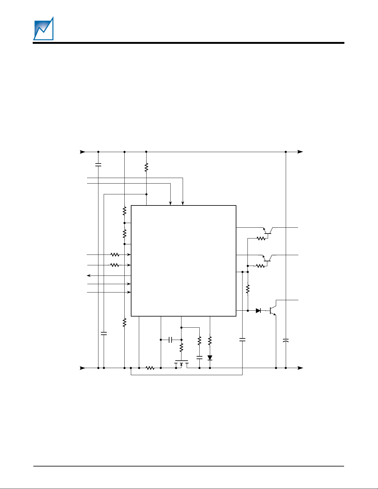
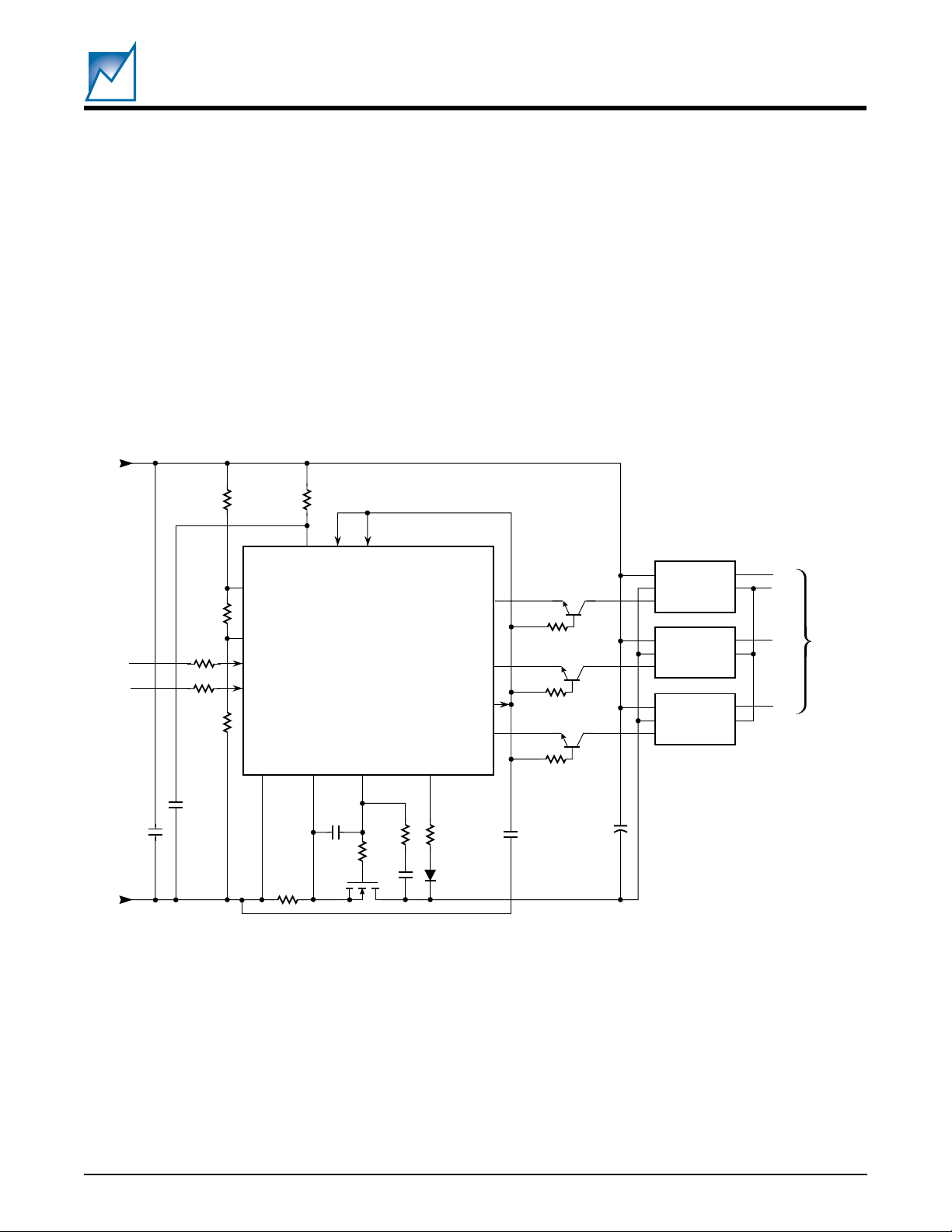
10 and 11 for connections.
SUMMIT MICROELECTRONICS, Inc.
2051 4.4 3/15/01
As long as the NVFL is set the FAULT# output will be
driven active. The Non-Volatile Fault Latch feature is
disabled in the default configuration.
7
Page 8
SMH4803A
Preliminary
V
DD
11 ≤ VDD ≤ 13
<t
PUVF
UV
OV
PD1#/
PD2#
VGATE
DRAIN
SENSE
CBSENSE
PG1#
5V
2.5V
50mV
REF
REF
t
PDD
VDD – V
t
GT
PGD
2.5V
<t
CBD
REF
V
DD
ENPGA
PG2#
ENPGB
PG3#
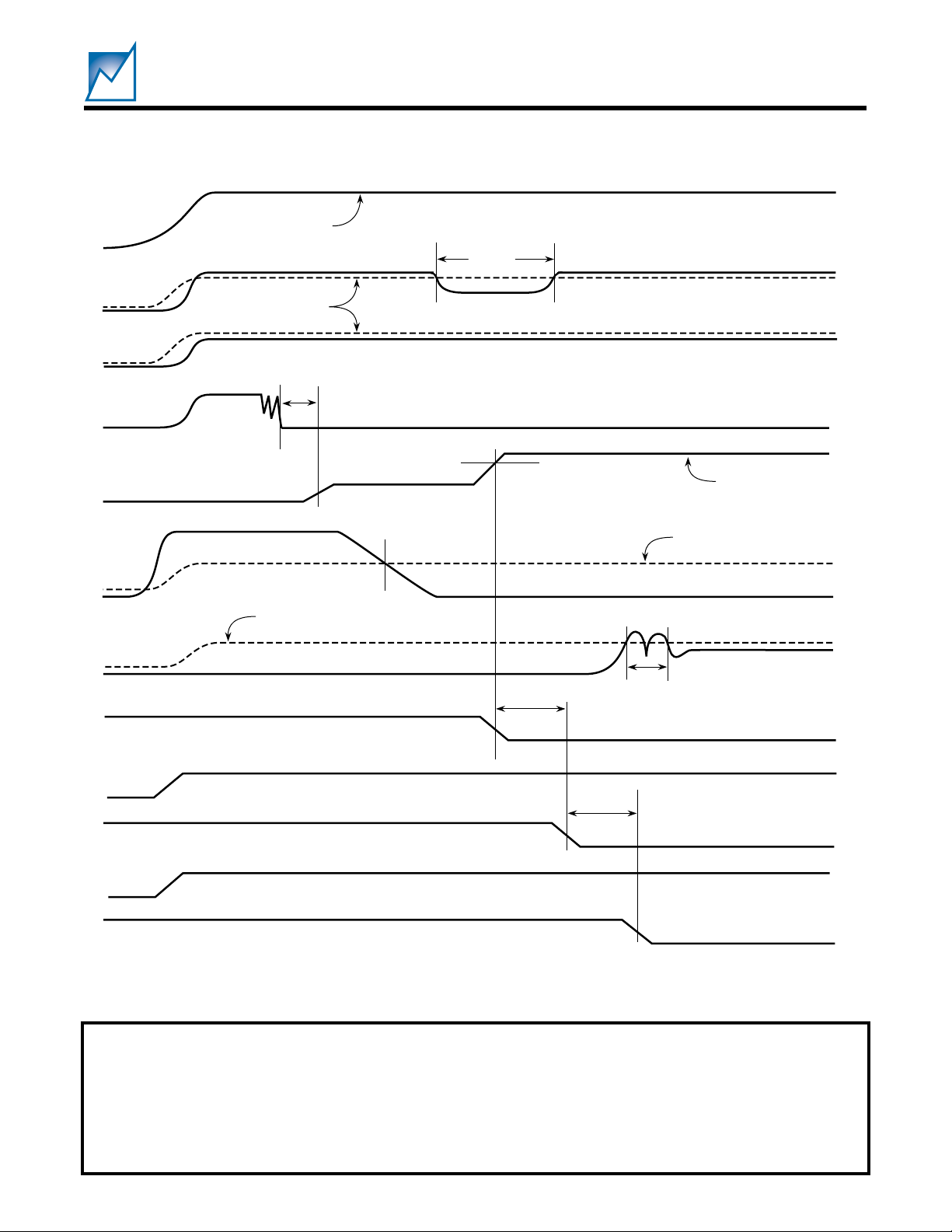
Figure 1. Complete Power On Timing Sequence
TIMING RELATIONSHIPS
Figure 1 illustrates some of the power on sequences,
including the UV and OV differentials to their reference,
and Power Good cascading.
8
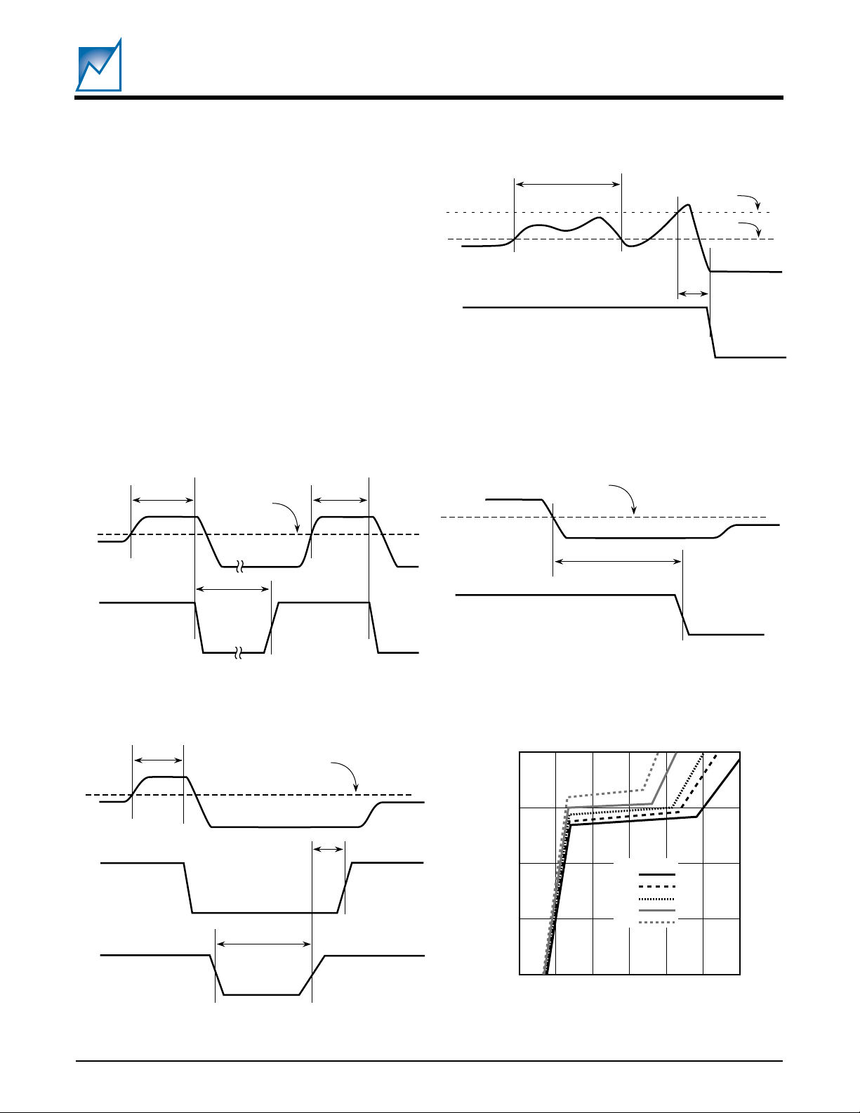
Figures 2, 3, and 4 indicate the affect on the VGATE
signal caused by different Circuit Breaker inputs. In
Figure 2 RESET# and MODE are high; in Figure 3
MODE is low. Figure 4 shows the Quick Trip mode.
2051 4.4 3/15/01
t
PGD
2051 Fig01 1.1
SUMMIT MICROELECTRONICS, Inc.
Page 9
SMH4803A
Preliminary
Resetting FAULT#
When the circuit breaker trips the VGATE output is turned
off and FAULT# is driven low. There are two methods to
reset the circuit breaker which are selectable with the
MODE pin. When MODE is held high or left floating the
circuit breaker is in the duty-cycle mode, and the breaker
resets automatically after a time of t
. When the MODE
CYC
pin is held low the circuit breaker can be reset by bringing
RESET# low. T
after bringing RESET# back high again
PDD
the VGATE output will attempt to restart the MOSFET slew
control circuitry. In either case, cycling power to the board
will also reset the circuit breaker. If the over current
condition still exists after the MOSFET switches back on
the circuit breaker will re-trip.
CBSENSE
T
CBD
50mV
T
CBD
<T
CBD
CBSENSE
VGATE
V
QCB
50mV
Figure 4. Circuit Breaker Timing — Quick Trip
2.5V
OV / UV
t
UOFLTR
T
FSTSHTDN
2051 Fig04 1.0
T
CYC
VGATE
2051 Fig02 1.0
Figure 2. Circuit Breaker Cycle Mode, RESET# High
CBSENSE
VGATE
RESET#
T
CBD
50mV
T
RST
T
PDD
2051 Fig03 1.0
FAULT#
Figure 5. Under-/Over-Voltage Filter Timing
13
12
(V)
DD
V
11
10
9
2
0
4
IDD (mA)
Temp, ºC
–40
0
25
85
125
68
2051 Fig05 2.0
10
12
2051 Fig06
Figure 3. Circuit Breaker Timing — Reset Mode
SUMMIT MICROELECTRONICS, Inc.
Figure 6. Effect of Temperature on Current Con-
2051 4.4 3/15/01
sumption Over Voltage Range
9
Page 10
PROGRAMMABLE FEATURES
SMH4803A
Preliminary
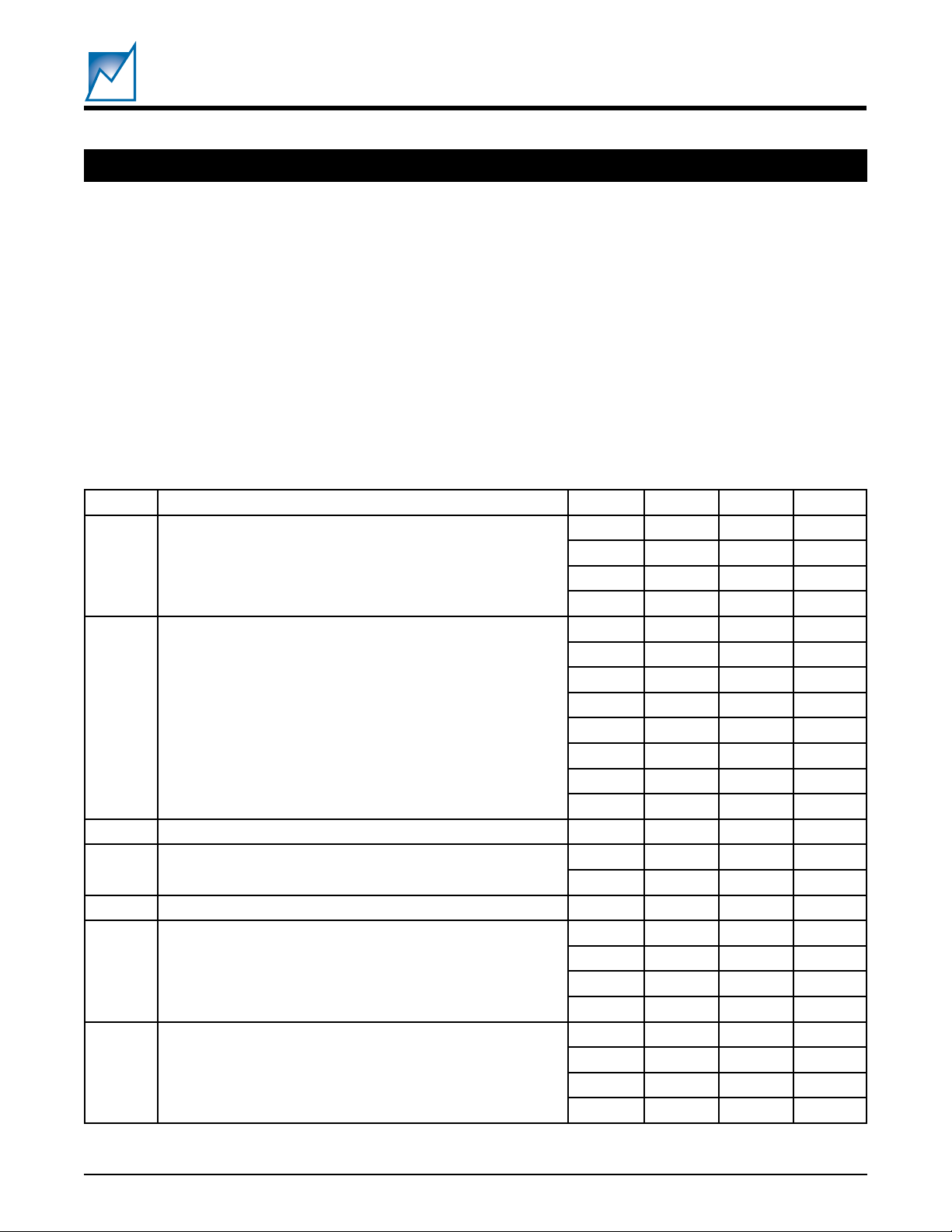
The SMH4803A has programmable time and voltage
functions that can be fine-tuned for a wide variety of
applications. Because of this a manufacturer can use a
common part type across a wide range of boards that are
used on a common host but have different electrical loads,
power-on timing requirements, host voltage monitoring
needs,
etc
. This ability shifts the focus of design away
from designing a new power interface for each board to
concentrating on the value added back-end logic. Because the programming is done at final test all combinations (all 128 possibilities) are readily available as off the
shelf stock items.
Pin Detect
The Pin Detect function can be enabled or disabled.
lobmySnoitpircseD.niM.pyT.xaMstinU
t
DBC
t
DGP
t
NDTHSTSF
t
CYC
t
TSR
t
FVUP
t
DDP
Note: * Denotes default configuration setting
htdiweslup#TESER002sn
)retlif(yaleDrekaerBtiucriCVm05
yaleDdooGrewoPelbammargorP
)3GPot2GP,2GPot1GP(
emitelcyCedomelcycrekaerbtiucriC
retlifegatloV-rednUelbammargorP
yaleDtceteDniPelbammargorP
Circuit Breaker Delay
The circuit breaker delay defines the period of time the
voltage drop across RS is greater than 50mV but less than
V
before the VGATE output will be shut down. This is
QCB
effectively a filter to prevent spurious shutdowns of
VGATE.
Power Good Delay
The PG delay timer that controls the delay from PG1# to
PG2#, and PG2# to PG3# being asserted.
Quick-Trip Circuit Breaker Threshold
This is the threshold voltage drop across R
that is placed
S
between VSS and CBSENSE.
004sµ
051sµ
*05sµ
5sµ
05sµ
052sµ
005sµ
5.1sm
*5sm
02sm
08sm
061sm
ffoETAGVottluafmorfyalednwoDtuhStsaF 002sn
*5.2s
5s
*ffO —
5sm
08sm
061sm
5.0sm
5sm
*08sm
061sm
2051 Prog Table 1.1
10
2051 4.4 3/15/01
SUMMIT MICROELECTRONICS, Inc.
Page 11

APPLICATIONS
SMH4803A
Preliminary
Operating at High Voltages
The breakdown voltage of the external active and passive
components limits the maximum operating voltage of the
SMH4803A hot-swap controller. Components that must
be able to withstand the full supply voltage are: the input
and output decoupling capacitors, the protection diode in
series with the DRAIN SENSE pin, the power MOSFET
switch and the capacitor connected between its drain and
gate, the high-voltage transistors connected to the power
good outputs, and the dropper resistor connected to the
controller’s VDD pin.
Over-Voltage and Under-Voltage Resistors
In the following examples, the three resistors, R1, R2, and
R3, connected to the OV and UV inputs, must be capable
of withstanding the maximum supply voltage of several
hundred volts. The trip voltage of the UV and OV inputs is
2.5V relative to V
. As the input impedance of UV and OV
SS
is very high, large value resistors can be used in the
resistive divider. The divider resistors should be high
stability, 1% metal-film resistors to keep the under-voltage
and over-voltage trip points accurate.
Telecom Design Example
A hot-swap telecom application may use a 48V power
supply with a –25% to +50% tolerance (
i.e.
, the 48V supply
can vary from 36V to 72V). The formulae for calculating
R1, R2, and R3 follow.
First a peak current, ID
, must be specified for the
MAX
resistive network. The value of the current is arbitrary, but
it can't be too high (self-heating in R3 will become a
problem), or too low (the value of R3 becomes very large,
and leakage currents can reduce the accuracy of the OV
and UV trip points). The value of ID
should be ≥200µA
MAX
for the best accuracy at the OV and UV trip points. A value
of 250µA for ID
will be used to illustrate the following
MAX
calculations.
With VOV (2.5V) being the over-voltage trip point, R1 is
calculated by the formula:
Next the minimum current that flows through the resistive
divider, ID
, is calculated from the ratio of minimum and
MIN
maximum supply voltage levels:
MIN
VS
MAX
.
×
ID VS
MAX MIN
=
ID
Substituting:
µ
72V
−
MIN UV
ID
MIN
×
µ
.
:
MIN
.
250 A 36V
==
ID 125 A
MIN
Now the value of R3 is calculated from ID
VS V
=
R3
VUV is the under-voltage trip point, also 2.5V. Substituting:
R3 268k
µ
125 A
.
−
36V 2.5V
==Ω
The closest standard 1% resistor value is 267kΩ
Then R2 is calculated:
V
+=
R1 R2
()
ID
UV
MIN
,
or
V
UV
=−
R2 R1
ID
MIN
.
Substituting:
2.5V
=−Ω=Ω−Ω=Ω
R2 10k 20k 10k 10k
µ
125 A
.
V
OV
=
R1
ID
MAX
.
Substituting:
2.5V
==Ω
R1 10k
SUMMIT MICROELECTRONICS, Inc.
µ
250 A
An Excel spread sheet is available on Summit's website
(
www.summitmicro.com
) to simplify the resistor value
calculations and tolerance analysis for R1, R2, and R3.
Dropper Resistor Selection
The SMH4803A is powered from the high-voltage supply
via a dropper resistor, RD. The dropper resistor must
.
provide the SMH4803A (and its loads) with sufficient
operating current under minimum supply voltage condi-
2051 4.4 3/15/01
11
Page 12

SMH4803A
Preliminary
tions, but must not allow the maximum supply current to be
exceeded under maximum supply voltage conditions.
The dropper resistor value is calculated from:
R
where VS
V
is the upper limit of the SMH4803A supply voltage,
DDMAX
MIN DD
=
D
II
DD LOAD
is the lowest operating supply voltage,
MIN
MAX
+
,
−
VS V
IDD is minimum current required for the SMH4803A to
operate, and I
is any additional load current from the
LOAD
2.5V and 5V outputs and between VDD and VSS.
The min/max current limits are easily met using the drop-
per resistor, except in circumstances where the input
voltage may swing over a very wide range (
e.g.
, input
varies between 20V and 100V). In these circumstances it
may be necessary to add an 11V zener diode between
VDD and VSS to handle the wide current range. The zener
voltage should be below the nominal regulation voltage of
the SMH4803A so that it becomes the primary regulator.
MOSFET VDS(ON) Threshold
The drain sense input on the SMH4803A monitors the
voltage at the drain of the external power MOSFET switch
with respect to VSS. When the MOSFET’s VDS is below the
user-defined threshold the MOSFET switch is considered
to be ON. The VDS(ON)
THRESHOLD
is adjusted using the
resistor, RT, in series with the drain sense protection
diode. This protection, or blocking, diode prevents high
voltage breakdown of the drain sense input when the
MOSFET switch is OFF. A low leakage MMBD1401 diode
offers protection up to 100V. For high voltage applications
(up to 500V) the Central Semiconductor CMR1F-10M
diode should be used. The VDS(ON)
THRESHOLD
is calcu-
lated from:
The voltage drop across the MOSFET switch and sense
resistor, V
VIRR
, is calculated from:
DSS
=+
DSS D S ON
()
,
where ID is the MOSFET drain current, RS is the circuit
breaker sense resistor, and RON is the MOSFET on
resistance.
VON V I R V
() ( )
where V
DS SENSE SENSE T DIODE
DIODE
THRESHOLD
is the forward voltage drop of the protection
diode. The VDS(ON)
due to the temperature dependence of V
The calculation below gives the VDS(ON)
=−×−
THRESHOLD
varies over temperature
DIODE
THRESHOLD
and I
SENSE
under
the worst case condition of 85°C ambient. Using a 68kΩ
resistor for RT gives:
VON 2.5V15A68k 0.5V1V
() ( )
DS
12
THRESHOLD
=− ×Ω−=
µ
2051 4.4 3/15/01
,
.
.
SUMMIT MICROELECTRONICS, Inc.
Page 13
SMH4803A
Preliminary
–48V
0V
10nF
100V
10kΩ
10kΩ
100nF
50V
R1
R3
R2
UV
OV
PD1#
PD2#
FAULT#
RESET#
MODE
SS
V
20mΩ
6.8kΩ
DD
V
R
S
R
D
2.5V
A
ENPG
B
ENPG
REF
SMH4803A
GATE
*10Ω
V
1kΩ
10nF
100V
CBSENSE
100nF
EN/TS
PG3#
PG2#
5V
REF
PG1#
DRAIN SENSE
R
T
68kΩ
MMBD1401
MMBTA06LT1
100kΩ
MMBTA06LT1
100kΩ
47kΩ
MMBTA06LT1
1N4148
100nF
50V
0V
100µF
100V
–48V
2051 Fig07
Figure 7. Changing Polarity of Power Good Output PG1#
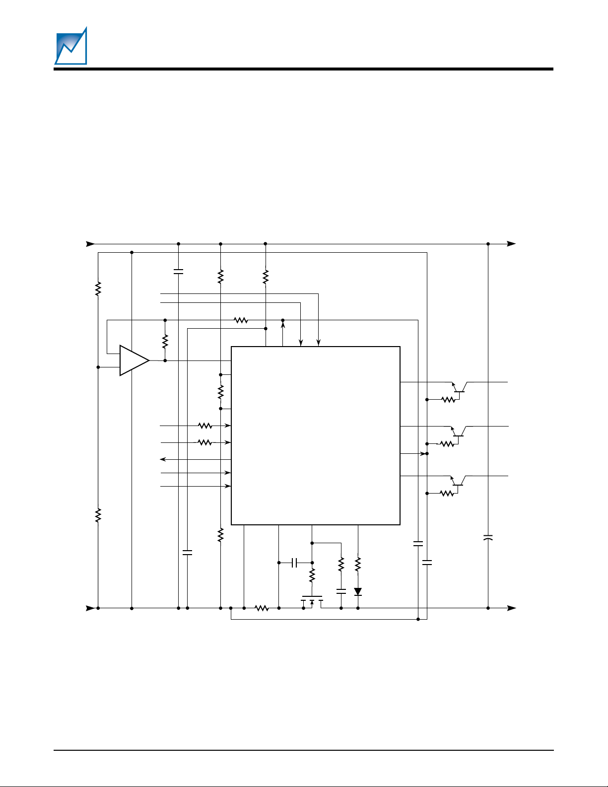
Note: Figures 7 through 11 — the *10Ω resistor must be located as close as possible to the MOSFET
SUMMIT MICROELECTRONICS, Inc.
2051 4.4 3/15/01
13
Page 14
SMH4803A
Preliminary
–48V
0V
NTC
50kΩ
@T
50kΩ
MAX
+
–
1MΩ
LMV331
10nF
100V
10kΩ
10kΩ
100nF
50V
R1
R3
R2
1kΩ
EN/TS
UV
OV
PD1#
PD2#
FAULT#
RESET#
MODE
SS
V
R
S
20mΩ
R
D
6.8kΩ
DD
REF
V
2.5V
SMH4803A
CBSENSE
100nF
*10Ω
A
ENPG
B
ENPG
GATE
V
1kΩ
10nF
100V
PG3#
PG2#
5V
REF
PG1#
DRAIN SENSE
100nF
50V
R
T
68kΩ
MMBD1401
0V
MMBTA06LT1
100kΩ
MMBTA06LT1
100kΩ
MMBTA06LT1
100kΩ
100µF
100V
100nF
50V
–48V
2051 Fig08
14
Figure 8. Overtemperature Shutdown
2051 4.4 3/15/01
SUMMIT MICROELECTRONICS, Inc.
Page 15
SMH4803A
Preliminary
EN1
EN2
EN3
EN4
–48V
0V
0V
10kΩ
10nF
100V
1MΩ
+
–
+
–
LMV
339
+
–
+
–
10kΩ
10kΩ
100nF
50V
R3
1kΩ
EN/TS
UV
R2
OV
PD1#
PD2#
FAULT#
RESET#
MODE
R1
SS
V
R
S
20mΩ
R
D
6.8kΩ
DD
REF
V
2.5V
SMH4803A
CBSENSE
100nF
*10Ω
A
ENPG
B
ENPG
GATE
V
1kΩ
10nF
100V
PG3#
PG2#
5V
REF
PG1#
DRAIN SENSE
100nF
50V
R
T
68kΩ
MMBD1401
MMBTA06LT1
100kΩ
MMBTA06LT1
100kΩ
MMBTA06LT1
100kΩ
100nF
50V
100µF
100V
–48V
2051 Fig09
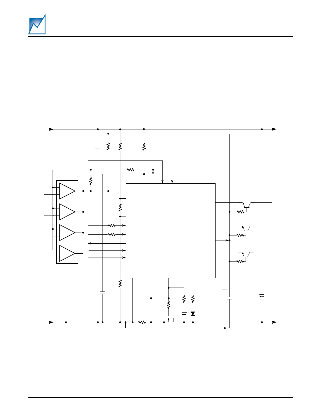
Figure 9. Expanding Input Monitoring Capability
Note: Figures 7 through 11 — the *10Ω resistor must be located as close as possible to the MOSFET
SUMMIT MICROELECTRONICS, Inc.
2051 4.4 3/15/01
15
Page 16
–48V
0V
10nF
100V
10kΩ
10kΩ
100nF
50V
R2
R1
R3
EN/TS
UV
OV
PD1#
PD2#
V
R
6.8kΩ
SS
R
D
S
DD
V
CBSENSE
100nF
A
B
ENPG
ENPG
SMH4803A
GATE
V
1kΩ
*10Ω
10nF
100V
PG3#
PG2#
5V
REF
PG1#
DRAIN SENSE
68kΩ
MMBD1401
MMBTA06LT1
100kΩ
MMBTA06LT1
100kΩ
MMBTA06LT1
100kΩ
100nF
50V
100µF
100V
DC / DC
Converters
+VIN
–VIN
ON/OFF
+VIN
–VIN
ON/OFF
+VIN
–VIN
ON/OFF
SMH4803A
Preliminary
+VOUT
–VOUT
+VOUT
–VOUT
+VOUT
–VOUT
2051 Fig10
V3
0V
V2
V1
ISOLATED
DC
OUTPUTS
16
Figure 10. Typical Application Sequencing Three DC/DC Converters
2051 4.4 3/15/01
SUMMIT MICROELECTRONICS, Inc.
Page 17
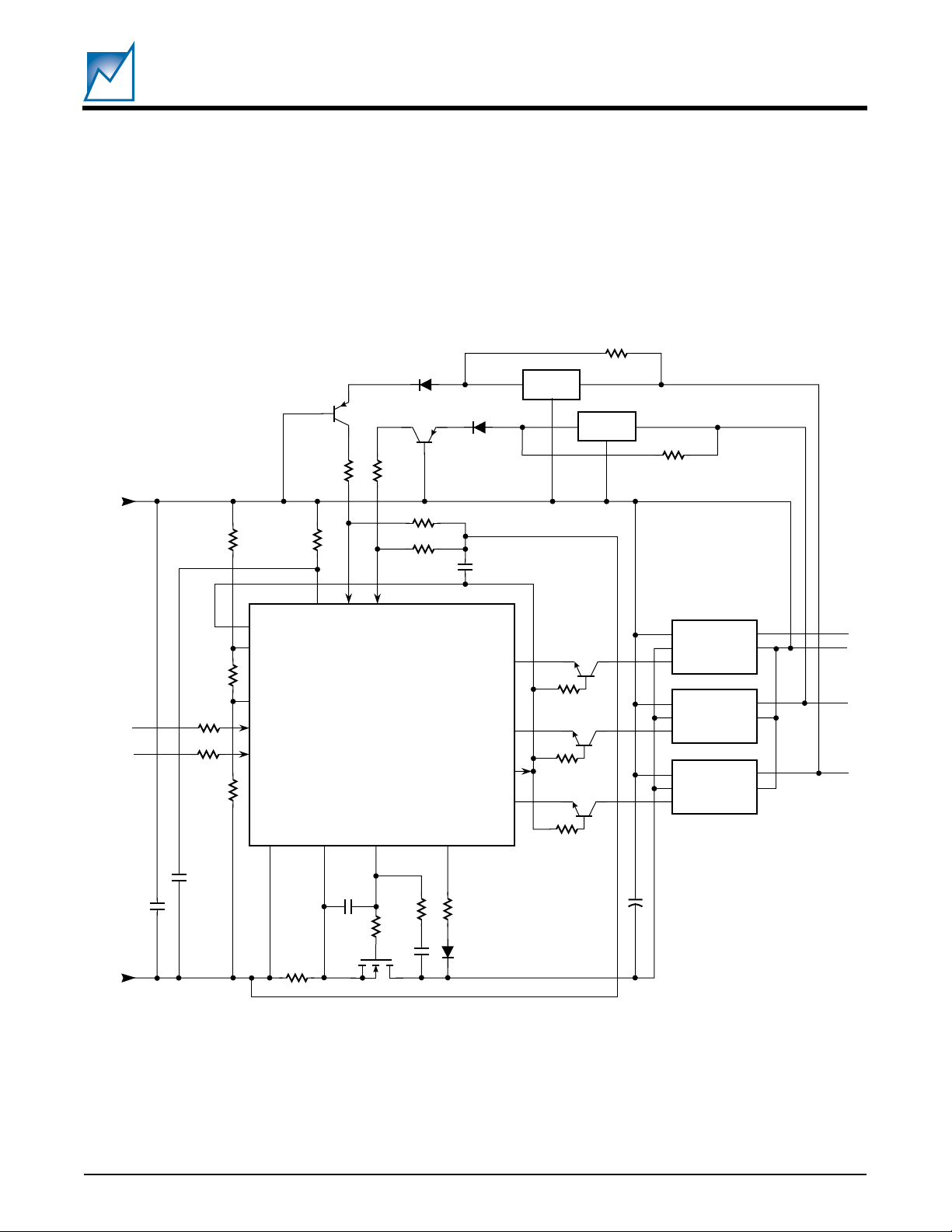
MMBTA56LT1
RESET1#
1N4148
MMBTA56LT1
1N4148
RESET2#
SMH4803A
Preliminary
RESET
RESET
–48V
0V
10nF
100V
10kΩ
10kΩ
100nF
50V
R3
R2
R1
EN/TS
UV
OV
PD1#
PD2#
R
6.8kΩ
SS
V
R
D
S
33kΩ
DD
V
CBSENSE
33kΩ
4.7kΩ
4.7kΩ
A
B
ENPG
ENPG
SMH4803A
GATE
V
100nF
1kΩ
*10Ω
10nF
100V
100nF
50V
PG3#
PG2#
5V
REF
PG1#
DRAIN SENSE
68kΩ
MMBD1401
100kΩ
100kΩ
100kΩ
Converters
+VIN
–VIN
ON/OFF
+VIN
–VIN
ON/OFF
+VIN
–VIN
ON/OFF
100µF
100V
DC / DC
+VOUT
–VOUT
+VOUT
–VOUT
+VOUT
–VOUT
2051 Fig11
V3
0V
V2
V1
Figure 11. Sequencing Converters with Common I/O Ground and Voltage Feedback
Note: Figures 7 through 11 — the *10Ω resistor must be located as close as possible to the MOSFET
SUMMIT MICROELECTRONICS, Inc.
2051 4.4 3/15/01
17
Page 18
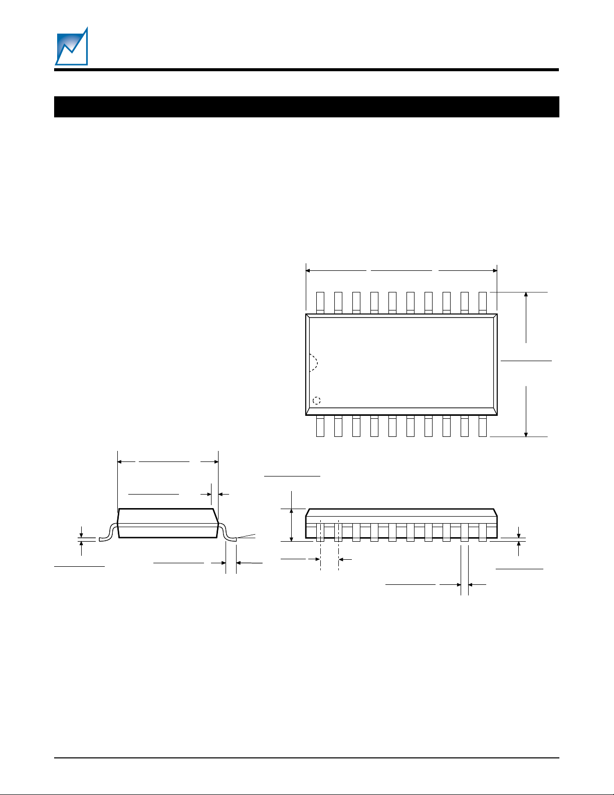
PACKAGE
20 PIN SOIC PACKAGE
SMH4803A
Preliminary
0.496 - 0.512
(12.60 - 13.00)
0.009 - 0.013
(0.23 - 0.32)
Ref. JEDEC MS-013
0.291 - 0.299
(7.40 - 7.60)
0.010 - 0.029
(0.25 - 0.75)
×45º
0.016 - 0.050
0.016 - 0.050
(0.40 - 1.27)
0 to 8
0 to 8
typ
typ
0.093 - 0.104
(2.35 - 2.65)
0.05
(1.27)
0.013 - 0.020
(0.33 - 0.51)
0.394 - 0.419
(10.00 - 10.65)
0.004 - 0.012
(0.10 - 0.30)
20Pin SOIC
18
2051 4.4 3/15/01
SUMMIT MICROELECTRONICS, Inc.
Page 19

ORDERING INFORMATION
SMH4803A
Preliminary
Base Part Number
SMH4803A
S
Package
S = SOIC
2051 T ree 2.0
NOTICE
SUMMIT Microelectronics, Inc. reserves the right to make changes to the products contained in this publication in
order to improve design, performance or reliability. SUMMIT Microelectronics, Inc. assumes no responsibility for
the use of any circuits described herein, conveys no license under any patent or other right, and makes no
representation that the circuits are free of patent infringement. Charts and schedules contained herein reflect
representative operating parameters, and may vary depending upon a user’s specific application. While the
information in this publication has been carefully checked, SUMMIT Microelectronics, Inc. shall not be liable for any
damages arising as a result of any error or omission.
SUMMIT Microelectronics, Inc. does not recommend the use of any of its products in life support or aviation applications
where the failure or malfunction of the product can reasonably be expected to cause any failure of either system or to
significantly affect their safety or effectiveness. Products are not authorized for use in such applications unless
SUMMIT Microelectronics, Inc. receives written assurances, to its satisfaction, that: (a) the risk of injury or damage has
been minimized; (b) the user assumes all such risks; and (c) potential liability of SUMMIT Microelectronics, Inc. is
adequately protected under the circumstances.
This document supersedes all previous versions.
© Copyright 2000 SUMMIT Microelectronics, Inc.
SUMMIT MICROELECTRONICS, Inc.
2051 4.4 3/15/01
19
 Loading...