

Page 1
r
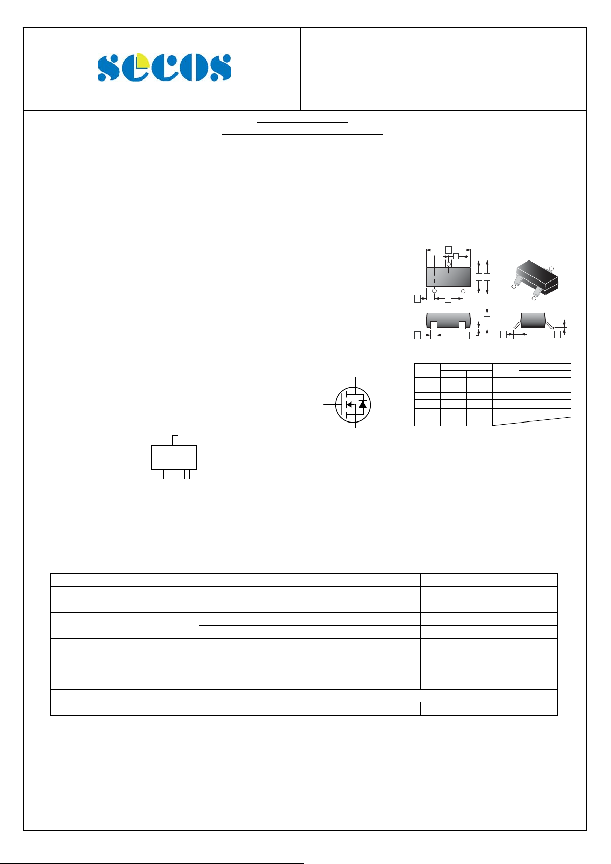
SMG2328
Elektronische Bauelemente
N-Channel Enhancement Mode Power MOSFET
RoHS Compliant Product
A Suffix of “-C” specifies halogen & lead-free
DESCRIPTION
The SMG2328 utilized advanced processing techniques to achieve the lowest
possible on-resistance, extremely efficient and cost-effectiveness device.
The SMG2328 is universally used for all commercial-industrial applications.
FEATURES
Simple drive requirement
Small package outline
Super high density cell design for extremely
low R
DS(ON)
DEVICE MARKING:
Drain
Gate
D
Source
2328
G S
MAXIMUM RATINGS (T
PARAMETER SYMBOL RATING UNIT
Drain – Source Voltage V
Gate – Source Voltage V
Continuous Drain Current 3
Pulsed Drain Current
Total Power Dissipation PD 1.38 W
Linear Derating Factor 0.01 W / °C
Operating Junction & Storage Temperature Range TJ, T
Thermal Resistance Junction-ambient 3 (Max.) R
1.2
= 25°C unless otherwise specified)
A
100 V
DSS
±20 V
GSS
T
=25°C ID 1.5 A
A
TA=70°C ID 1.2 A
I
6 A
DM
-55~150 °C
STG
THERMAL DATA
90 °C / W
θJA
100V, 250mΩ, 1.5A
A
L
3
Top View
1
K E
F
REF.
Millimeter
Min. Max. Min. Max.
A 2.70 3.10 G 0.10 REF.
B 2.25 3.00 H 0.40 REF.
C 1.30 1.70 J 0.10 0.20
D 1.00 1.40 K 0.45 0.55
E 1.70 2.30 L 0.85 1.15
F 0.35 0.50
SC-59
C B
2
D
G
1
2
H J
REF.
Millimete
3
http://www.SeCoSGmbH.com/ Any changes of specification will not be informed individually.
01-Jun-2010 Rev. A Page 1 of 4
Page 2
Elektronische Bauelemente
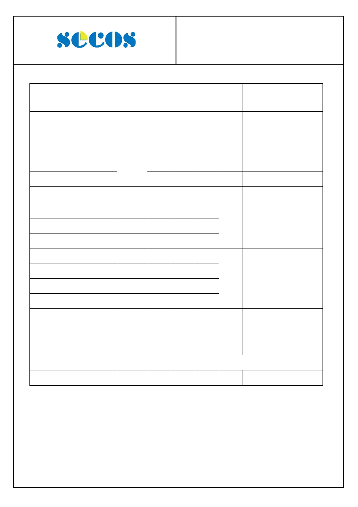
ELECTRICAL CHARACTERISTICS (T
PARAMETER SYMBOL MIN TYP MAX UNIT TEST CONDITION
N-Channel Enhancement Mode Power MOSFET
= 25°C unless otherwise specified)
J
SMG2328
100V, 250mΩ, 1.5A
Drain-Source Breakdown Voltage BV
Gate Threshold Voltage V
100 - - V VGS=0V, ID =250μA
DSS
1 - 2.5 V VDS= V
GS(th)
GS, ID
=250μA
Forward Transconductance gfs - 4 - S VDS=15V, ID =1.5A
Gate-Source Leakage Current I
Drain-Source Leakage
Current(T
=25°C)
J
Drain-Source Leakage
Current(T
=55°C)
J
Drain-Source On-State Resistance R
Total Gate Charge 2 Q
Gate-Source Chagre Qgs - 4.4 -
- - ±100 nA VGS=±20V
GSS
- - 1 μA V
I
DSS
- - 10 μA V
- - 250 mΩ VGS=10V, ID=1.5A
DS(ON)
- 11.1 -
g
nC V
=80V, VGS=0V
DS
=80V, VGS=0V
DS
=80V, ID =1.5A, VGS=5V
DS
Gate-Drain (“Miller”) Change Qgd - 3 -
Turn -on Delay Ti me 2 T
Rise Time Tr - 9.4 -
Turn-off Delay Time T
- 9 -
d(ON)
- 26.8 -
d(OFF)
nS
V
=30V, VGS=10V
DD
=1A, RL=30Ω, RG=6Ω
I
D
Fall Time Tf - 2.6 -
Input Capacitance C
Output Capacitance C
Reverse Transfer Capacitance C
- 975 -
ISS
- 38 -
OSS
- 27 -
RSS
SOURCE-DRAIN DIODE
Forward On Voltage 2 V
- - 1.2 V IS=1.0A, VGS=0V
SD
Notes:
1. Pulse width limited by Max. junction temperature.
2. Pulse width ≦ 300 μs, duty cycle ≦ 2%.
3. Surface mounted on 1 in
2
copper pad of FR4 board;270 °C / W when mounted on Min. copper pad.
pF
V
=25V
DS
=0V
V
GS
f=1MHz
http://www.SeCoSGmbH.com/ Any changes of specification will not be informed individually.
01-Jun-2010 Rev. A Page 2 of 4
Page 3
Elektronische Bauelemente
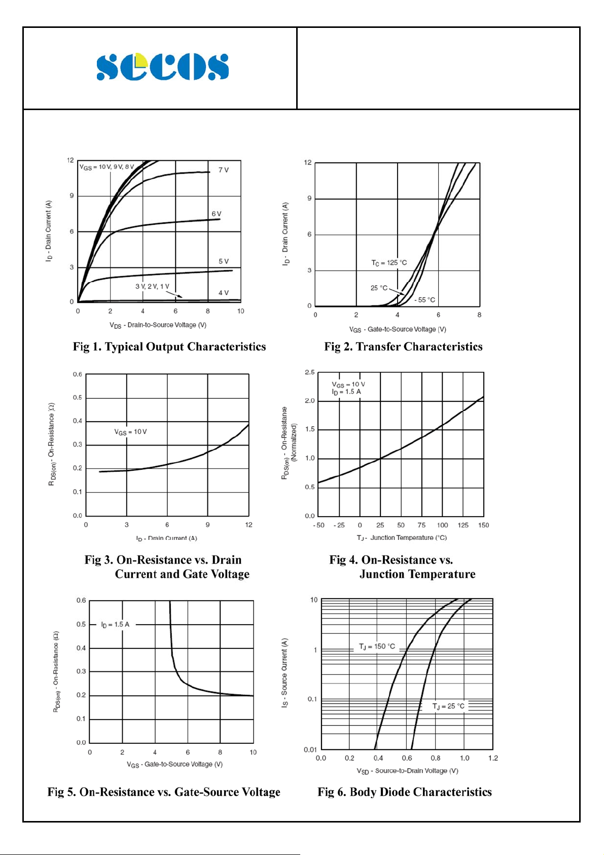
CHARACTERISTIC CURVES
SMG2328
N-Channel Enhancement Mode Power MOSFET
100V, 250mΩ, 1.5A
http://www.SeCoSGmbH.com/ Any changes of specification will not be informed individually.
01-Jun-2010 Rev. A Page 3 of 4
Page 4
Elektronische Bauelemente
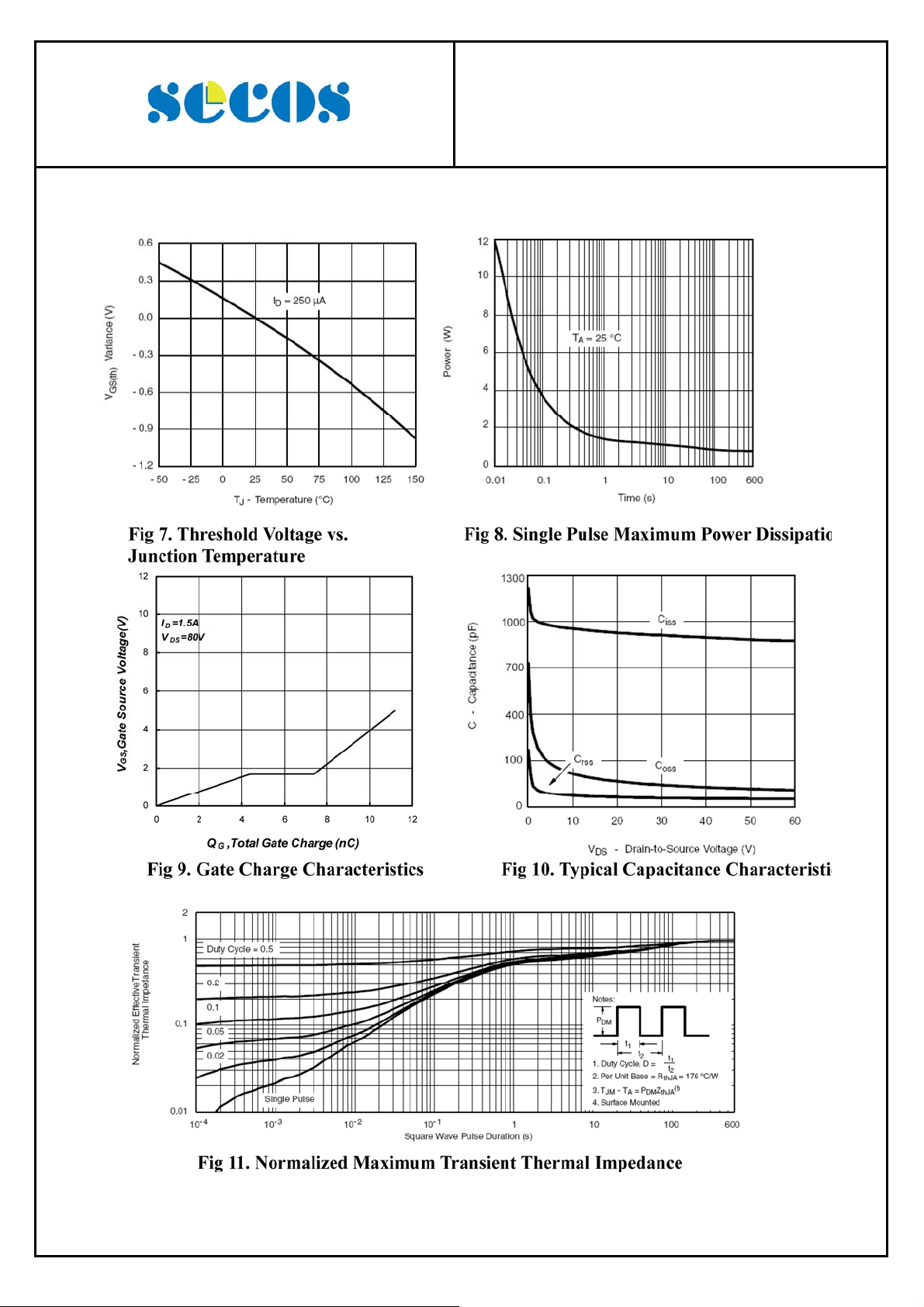
CHARACTERISTIC CURVES
SMG2328
N-Channel Enhancement Mode Power MOSFET
100V, 250mΩ, 1.5A
http://www.SeCoSGmbH.com/ Any changes of specification will not be informed individually.
01-Jun-2010 Rev. A Page 4 of 4
 Loading...