

Page 1
TC74HC123AP/AF/AFN
TOSHIBA CMOS Digital Integrated Circuit Silicon Monolithic
TC74HC123AP,TC74HC123AF,TC74HC123AFN
Dual Retriggerable Monostable Multivibrator
The TC74HC123A is a high speed CMOS MONOSTABLE
MULTIVIBRATOR fabricated with silicon gate C
technology.
It achieves the high speed operation similar to equivalent
LSTTL while maintaining the CMOS low power dissipation.
There are two trigger inputs,
input (positive edge). These inputs are valid for a slow rise/fall
time signal (tr = tf = 1 s) as they are schmitt trigger inputs. This
device may also be triggered by using
edge).
After triggering, the output stays in a MONOSTABLE state for
a time period determined by the external resistor and capacitor
(Rx, Cx ). A low level at the
MONOSTABLE state, if a new trigger is applied, it extends the
MONOSTABLE period (retrigger mode).
Limits for Cx and Rx are:
External capacitor, Cx: No limit
External resistor, Rx: V
V
All inputs are equipped with protection circuits against static
discharge or transient excess voltage.
A input (negative edge), and B
CLR
input breaks this state. In the
CLR
= 2.0 V more than 5 kΩ
CC
≥ 3.0 V more than 1 kΩ
CC
2
MOS
input (positive
Features (Note)
Note: xxxFN (JEDEC SOP) is not avail abl e in
Japan.
TC74HC123AP
TC74HC123AF
• High speed: t
• Low power dissipation
Standby state: I
Active state: I
• High noise immunity: V
• Output drive capability: 10 LSTTL loads
• Symmetrical output impedance: |I
• Balanced propagation delays: t
• Wide operating voltage range: V
• Pin and function compatible with 74LS123
Note: In the case of using only one circuit,
= 25 ns (typ.) at VCC = 5 V
pd
= 4 µA (max) at Ta = 25°C
CC
= 700 µA (max) at Ta = 25°C
CC
= V
NIH
tied to GND, Rx/Cx
the other inputs should be tied to V
・Cx・Q・
= 28% VCC (min)
NIL
| = IOL = 4 mA (min)
OH
∼
t
−
pLH
pHL
(opr) = 2 to 6 V
CC
should be tied to OPEN,
Q
CLR
or GND.
CC
TC74HC123AFN
should be
Weight
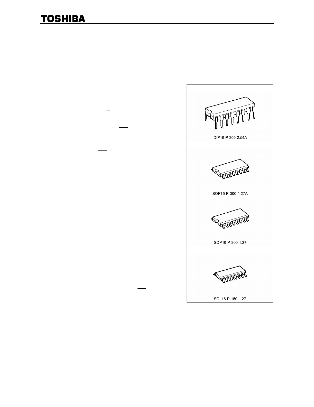
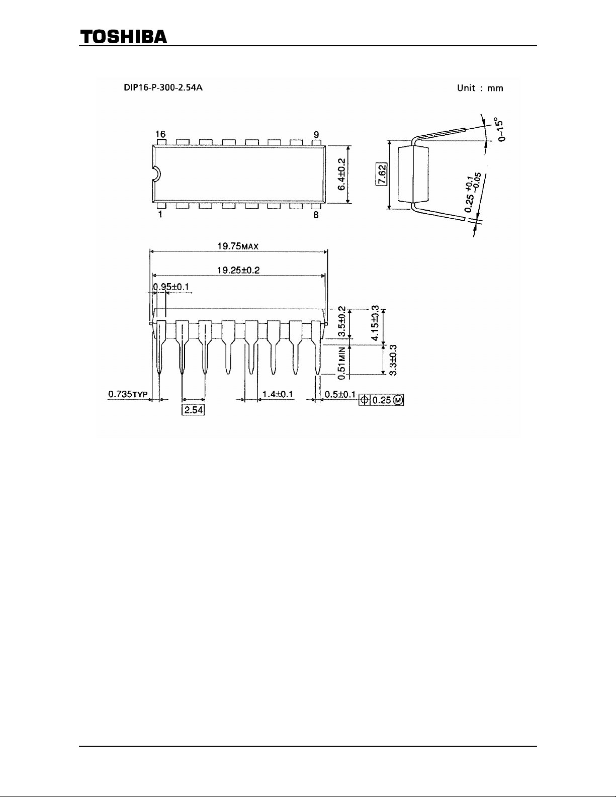
DIP16-P-300-2.54A : 1.00 g (typ.)
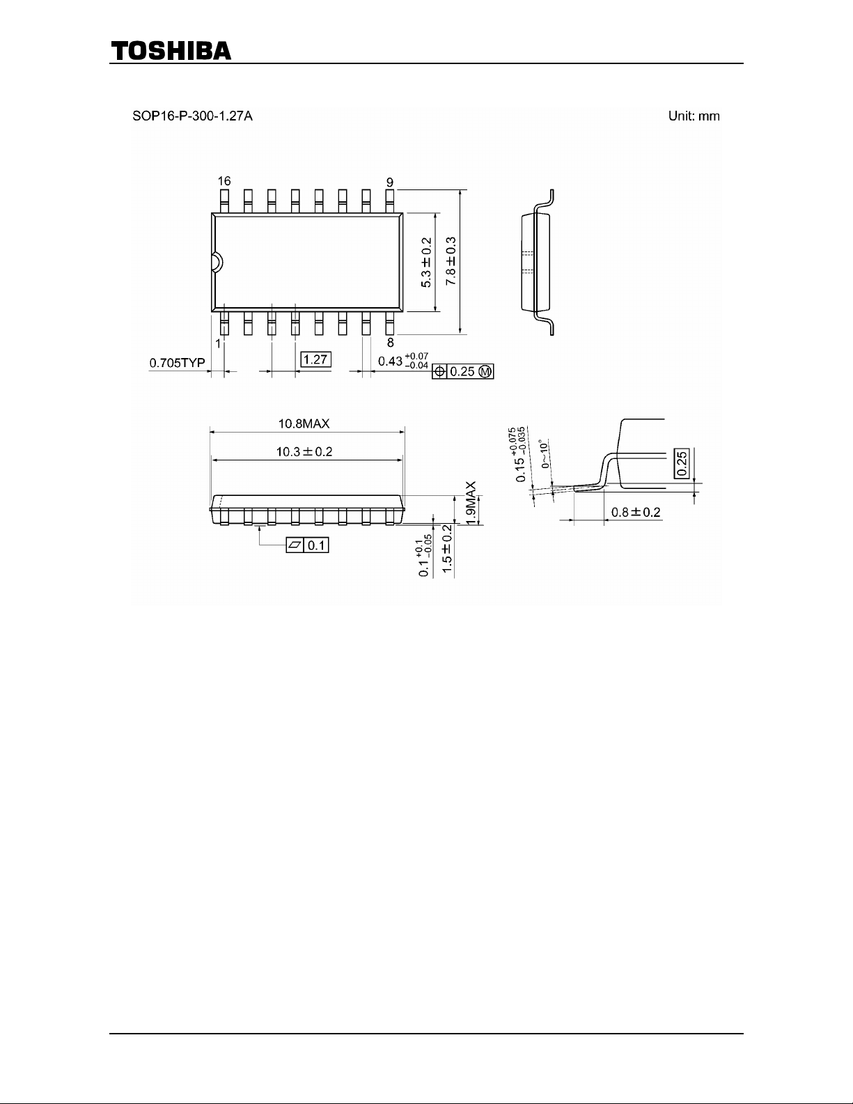
SOP16-P-300-1.27A : 0.18 g (typ.)
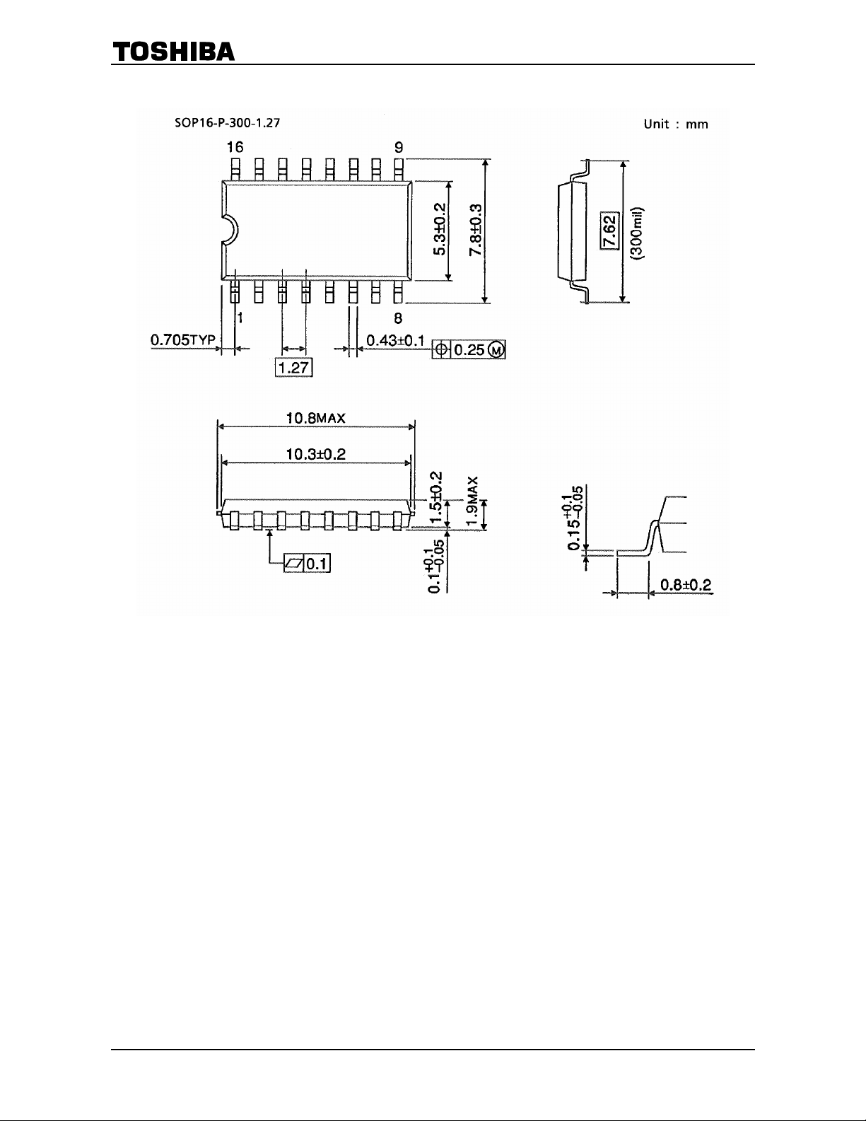
SOP16-P-300-1.27 : 0.18 g (typ.)
SOL16-P-150-1.2 7 : 0.13 g (typ.)
1
2006-06-01
Page 2
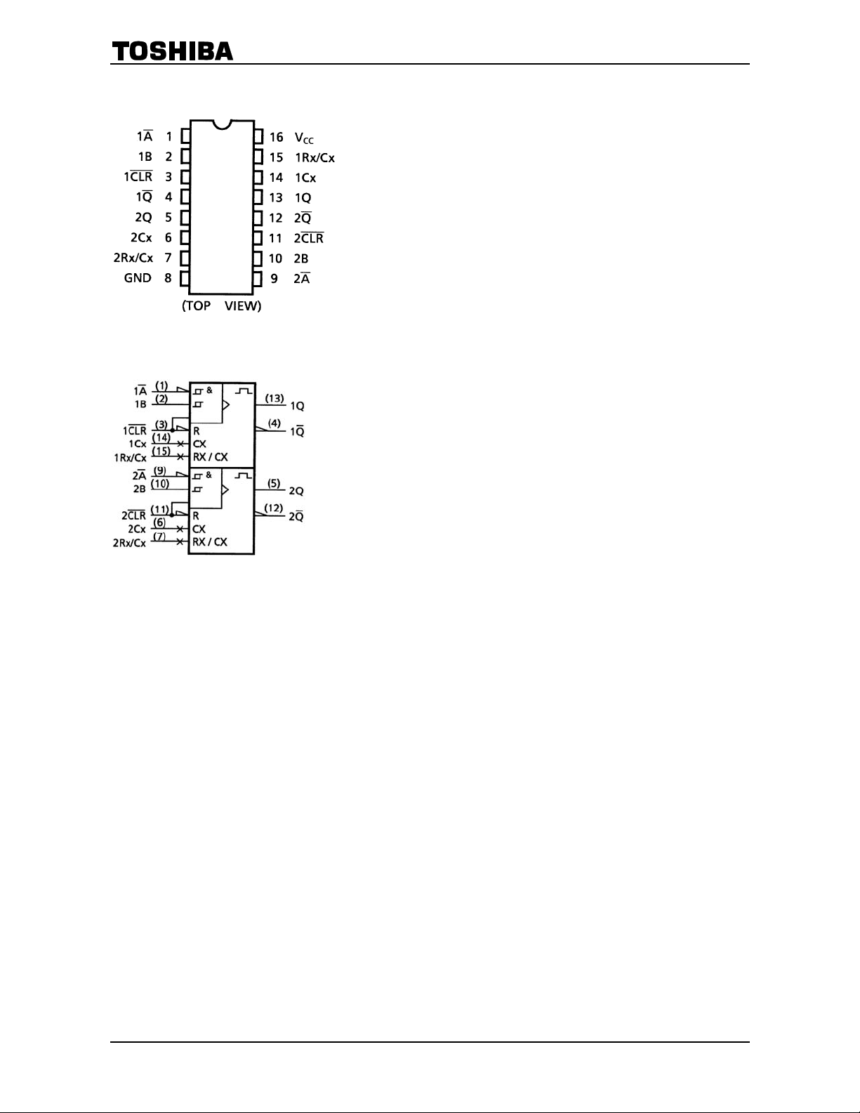
Pin Assignment
IEC Logic Symbol
TC74HC123AP/AF/AFN
2
2006-06-01
Page 3
TC74HC123AP/AF/AFN
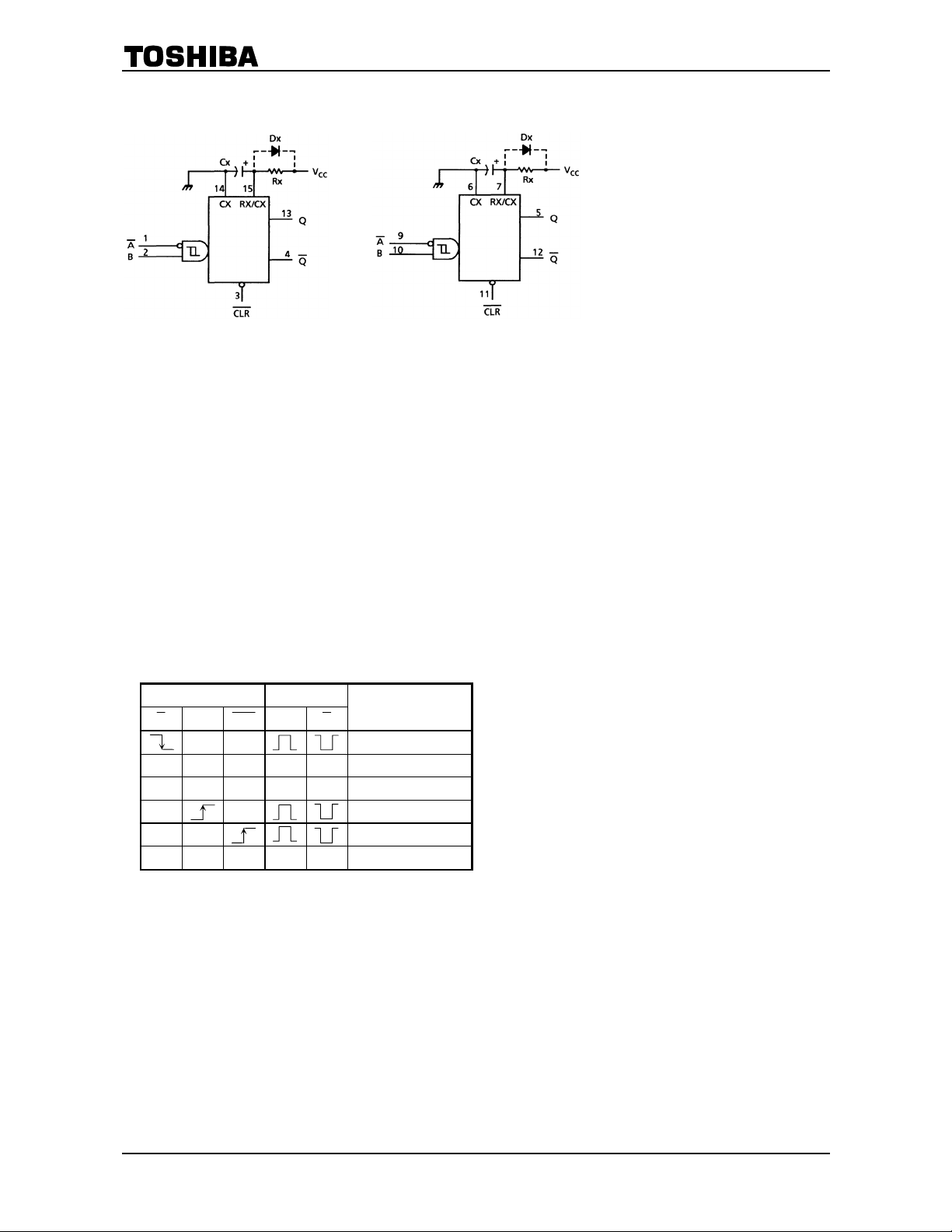
Block Diagram (Note 1)(Note 2)
Note 1: Cx, Rx, Dx are external
capacitor, resistor, and diode, respectively.
Note 2: External clamping diode, Dx;
The external capacitor is charged to V
If the supply voltage is turned off, Cx is discharges mainly through the inter nal (par asi t i c) diode. If Cx is
sufficiently large and V
current or latch-up. If the capacitance of the supply voltage filter i s large enough an d V
in rush current is automatically limited and damage to the IC is avoided.
The maximum value of forward current through the parasi t ic diode is
In the case of a large Cx, the limit of fall time of the supply voltage is determined as follows:
≥ (VCC − 0.7) Cx/20 mA
t
f
(tf is the time between the supply voltage turn off and the supply voltage reac hin g 0.4 V
In the event a system does not satisfy the above condition, an external clamping diode (D x) is needed to
protec t the IC f rom in rush current.
drops rapidly, there will be some possibility of damaging the IC through in rush
CC
Truth Tabl e
level in the wait state, i.e. when no trigger is applied.
CC
CC
±20 mA.
drops slowly, the
.)
CC
Inputs Outputs
B
A
H H Output Enable
X L H L H Inhibit
H X H L H Inhibit
L H Output Enable
L H Output Enable
X X L L H Inhibit
X: Don’t care
Q Q
CLR
Function
3
2006-06-01
Page 4
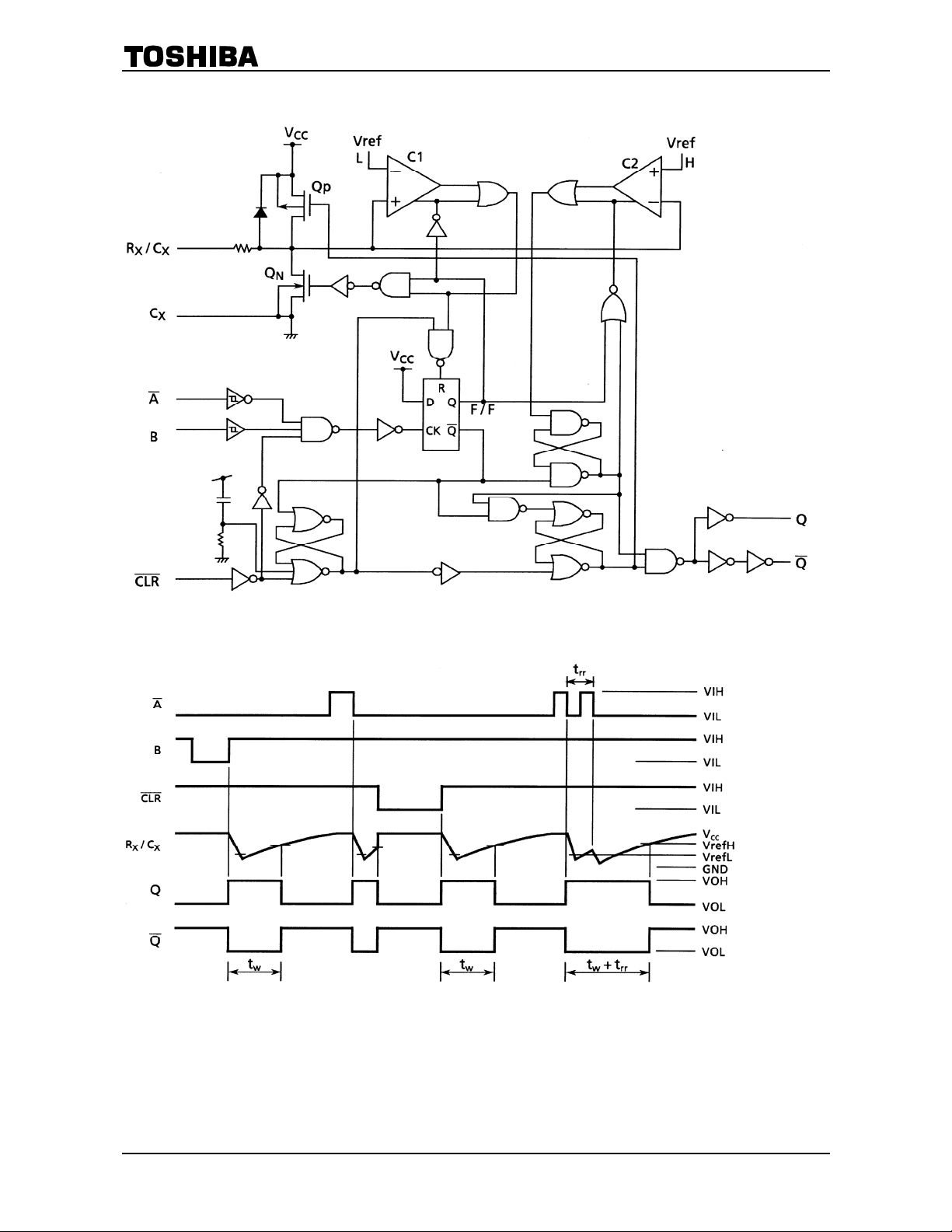
System Diagram
TC74HC123AP/AF/AFN
Timing Chart
4
2006-06-01
Page 5
Functional Description
(1) Stand-by state
The external capacitor (Cx) is fully charged to V
triggering, the Q
comparators that relate to the timing of the output pulse, and two reference voltage supplies turn off.
The total supply current is only leakage current.
(2) Trigger operation
Trigger operation is effective in any of the following three cases. First, the condition where the
input is low, and the B input has a rising signal; second, where the B input is high, and the
has a falling signal; and third, where the
input has a rising signal.
After a trigger becomes effective, comparators C1 and C2 start operating, and Q
external capacitor discharges through Q
voltage level falls to the internal reference voltage Vref L, the output of C1 becomes low. The flip-flop
is then reset and Q
After Q
constant of external capacitor Cx and resistor Rx.
Upon triggering, output Q becomes high, following some delay time of the internal F/F and gates. It
stays high even if the voltage of Rx/Cx changes from falling to rising. When Rx/Cx reaches the
internal reference voltage Vref H, the output of C2 becomes low, the output Q goes low and C2 stops
its operation. That means, after triggering, when the voltage level of the Rx/Cx node reaches Vref H,
the IC returns to its MONOSTABLE state.
With large values of Cx and Rx, and ignoring the discharge time of the capacitor and internal
delays of the IC, the width of the output pulse, tw (OUT), is as follows:
Retrigger operation
(3)
When a new trigger is applied to either input
effective only if the IC is charging Cx. The voltage level of the Rx/Cx node then falls to Vref L level
again. Therefore the Q output stays high if the next trigger comes in before the time period set by Cx
and Rx.
If the new trigger is very close to previous trigger, such as an occurrence during the discharge cycle,
it will have no effect.
The minimum time for a trigger to be effective 2nd trigger, trr (Min.), depends on V
Reset operation
(4)
In normal operation, the
the Q output is held low and the trigger control F/F is reset. Also, Q
rapidly to V
This means if
turns off, the voltage at the Rx/Cx node starts rising at a rate determined by the time
N
tw (OUT)
= 1.0 Cx Rx
.
CC
TC74HC123AP/AF/AFN
in the stand-by state. That means, before
CC
and QN transistors which are connected to the Rx/Cx node are in the off state. Two
P
input
A
input is low and the B input is high, and the
A
. The voltage level at the Rx/Cx node drops. If the Rx/Cx
N
turns off. At that moment C1 stops but C2 continues operating.
N
or B while in the MONOSTABLE state, it is
A
input is held high. If
CLR
is set low, the IC goes into a wait state.
CLR
is low, a trigger has no effect because
CLR
turns on and Cx is charged
P
is turned on. The
N
and Cx.
CC
CLR
A
5
2006-06-01
Page 6
TC74HC123AP/AF/AFN
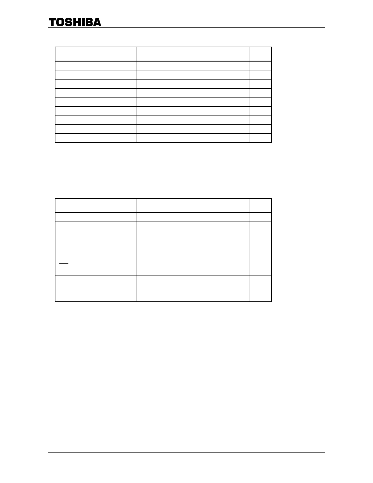
Absolute Maximum Ratings (Note 1)
Characteristics Symbol Rating Unit
Supply voltage range VCC −0.5 to 7 V
DC input voltage VIN −0.5 to VCC + 0.5 V
DC output voltage V
Input diode current IIK ±20 mA
Output diode current IOK ±20 mA
DC output current I
DC VCC/ground current ICC ±50 mA
Power dissipation PD 500 (DIP) (Note 2)/180 (SOP) mW
Storage temperature T
Note 1: Exceeding any of the absolute m aximum ratings, even briefly, lead to deterioration in IC performance or
even destruction.
Note 2: 500 mW in the range of Ta
applied until 300 mW.
Recommended Operati ng Co nditions (Note 1)
−0.5 to VCC + 0.5 V
OUT
±25 mA
OUT
−65 to 150 °C
stg
= −40 to 65°C. From Ta = 65 to 85°C a derating factor of −10 mW/°C shall be
Characteristics Symbol Rating Unit
Supply voltage VCC 2 to 6 V
Input voltage VIN 0 to V
Output voltage V
Operating temperature T
Input rise and fall time
CLR only)
(
External capacitor Cx No limitation (Note 2) F
External resistor Rx
0 to V
OUT
opr
0 to 1000 (V
t
, tf
r
0 to 500 (V
0 to 400 (V
≥5 k (V
≥1 k (V
CC
CC
−40 to 85 °C
= 2.0 V)
CC
= 4.5 V)
CC
= 6.0 V)
CC
= 2.0 V) (Note 2)
CC
≥ 3.0 V) (Note 2)
CC
V
V
ns
Ω
Note 1: The recommended operating condit i ons ar e required to ensure the normal operation of the device.
Unused inputs must be tied to either VCC or GND.
Note 2: The maximum allowable valu es of Cx and Rx are a functi on of leak age of c apaci t or Cx, the leakag e of
TC74HC123A, and leakage due to board layout and surface resistance.
Susceptibility to externally induced noise signals may occur for Rx
> 1 MΩ.
6
2006-06-01
Page 7
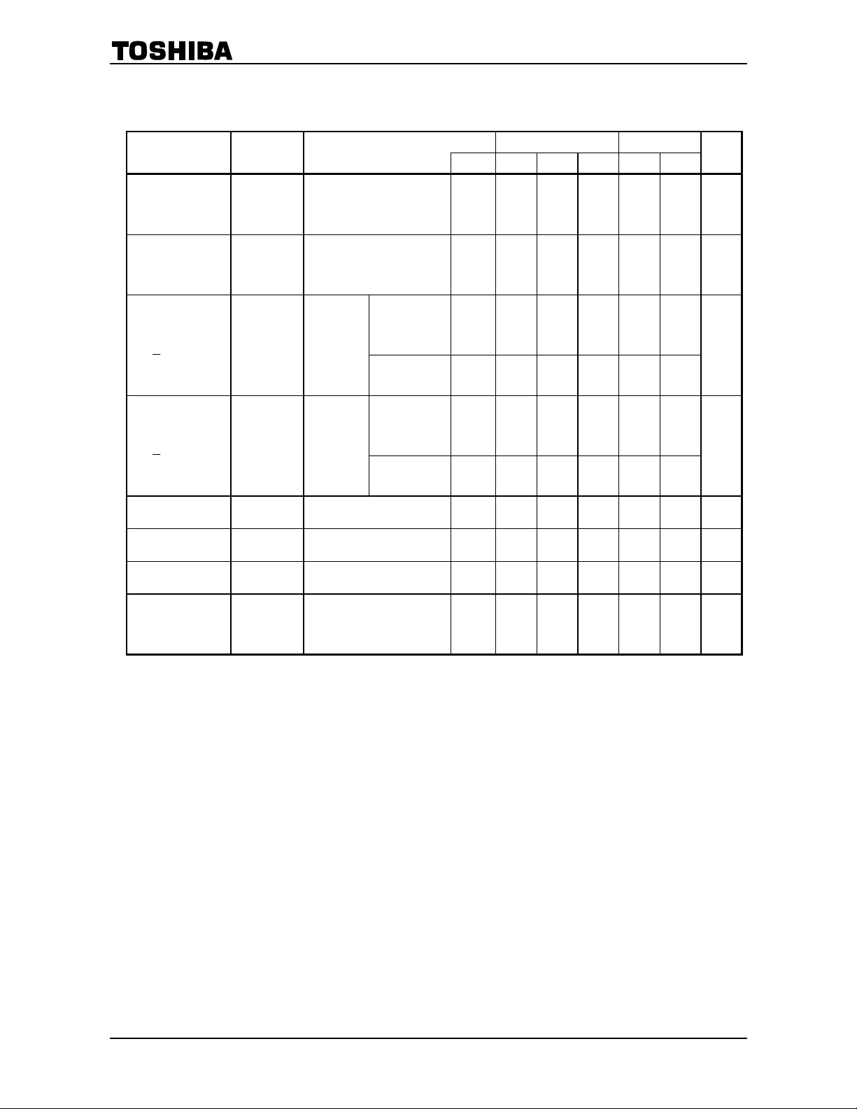
Electrical Characteristics
DC Characteristics
TC74HC123AP/AF/AFN
Characteristics Symbol
High-level input
voltage
Low-level input
voltage
High-level output
voltage
)
(Q,
Q
Low-level output
voltage
)
(Q,
Q
Input leakage
current
Rx/Cx terminal
off-state current
Quiescent supply
current
Active-state supply
current
(Note)
V
V
V
V
I
I
OH
OL
I
IN
I
IN
CC
CC
IH
IL
Test Condition Ta = 25°C Ta = −40 to 85°C
V
⎯
⎯
or V
or V
= 0.5 V
IOH = −20 µA
IL
IOH = −4 mA
= −5.2 mA
I
OH
IOL = 20 µA
IL
IOL = 4 mA
I
= 5.2 mA
OL
CC
V
IN
= V
IH
V
IN
= V
IH
VIN = VCC or GND 6.0 ⎯ ⎯ ±0.1 ⎯ ±1.0 µA
VIN = VCC or GND 6.0 ⎯ ⎯ ±0.1 ⎯ ±1.0 µA
VIN = VCC or GND 6.0 ⎯ ⎯ 4.0 ⎯ 40.0 µA
VIN = VCC or GND
Rx/Cx
CC
2.0
4.5
6.0
2.0
4.5
6.0
2.0
4.5
6.0
4.5
6.0
2.0
4.5
6.0
4.5
6.0
2.0
4.5
6.0
(V)
Min Typ. Max Min Max
1.50
3.15
4.20
⎯
⎯
⎯
1.9
4.4
5.9
4.18
5.68
⎯
⎯
⎯
⎯
⎯
⎯
⎯
⎯
⎯
⎯
⎯
⎯
⎯
⎯
2.0
4.5
6.0
4.31
5.80
0.0
0.0
0.0
0.17
0.18
45
400
0.7
⎯
⎯
⎯
0.50
1.35
1.80
⎯
⎯
⎯
⎯
⎯
0.1
0.1
0.1
0.26
0.26
200
500
1.0
1.50
3.15
4.20
⎯
⎯
⎯
1.9
4.4
5.9
4.13
5.63
⎯
⎯
⎯
⎯
⎯
⎯
⎯
⎯
⎯
⎯
⎯
0.50
1.35
1.80
⎯
⎯
⎯
⎯
⎯
0.1
0.1
0.1
0.33
0.33
260
650
1.3
Unit
V
V
V
V
µA
µA
mA
Note: Per circuit
7
2006-06-01
Page 8
TC74HC123AP/AF/AFN
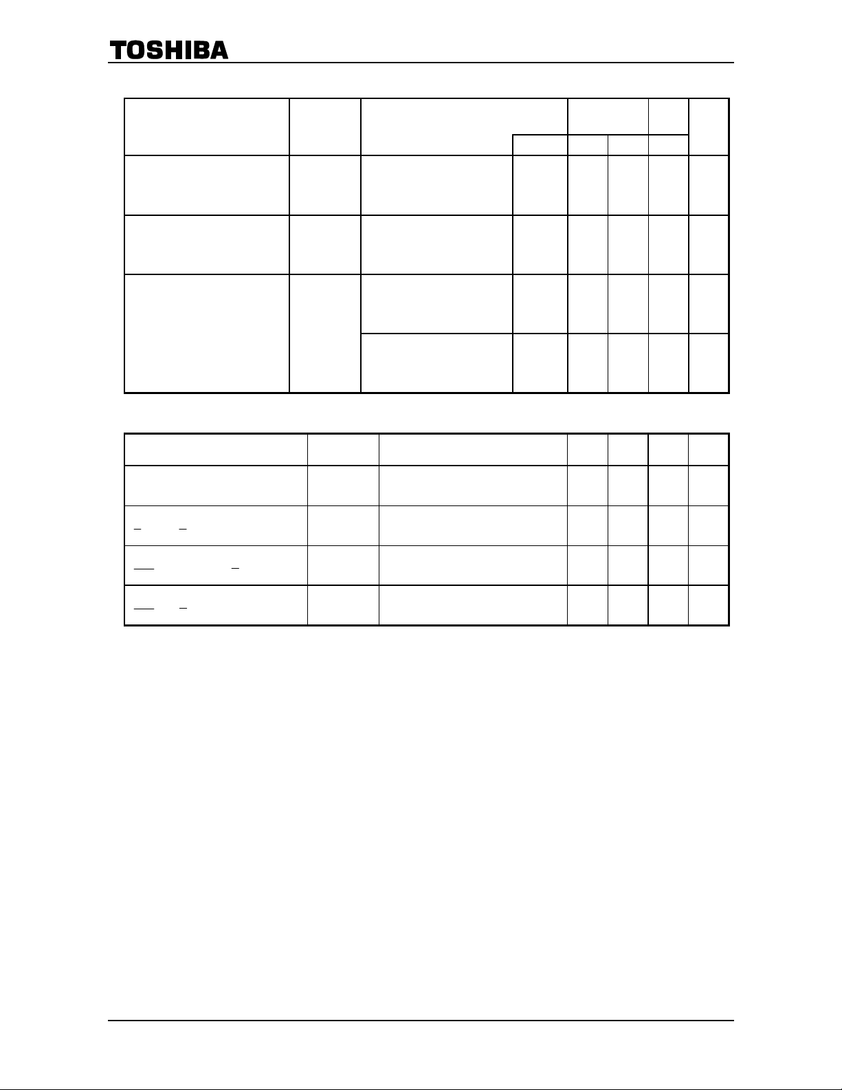
Timing Requirements (input: t
Characteristics Symbol
Minimum pulse width
Minimum clear width t
Minimum retrigger time trr
AC Characteristics
Characteristics Symbol Test Condition Min Typ. Max Unit
Output transition time
Propagation delay time
(
, B-Q, Q)
A
Propagation delay time
CLR TRIGGER-Q, Q)
(
Propagation delay time
(
CLR -Q, Q)
(CL = 15 pF, VCC = 5 V, Ta = 25°C, input: tr = tf = 6 ns)
= tf = 6 ns)
r
t
W (L)
t
W (H)
W (L)
t
TLH
t
THL
t
pLH
t
pHL
t
pLH
t
pHL
t
pLH
t
pHL
Rx = 1 kΩ
= 100 pF
Cx
Rx
= 1 kΩ
= 0.01 µF
Cx
Ta
Test Condition Ta = 25°C
V
⎯
⎯
(V) Typ. Limit Limit
CC
2.0
4.5
6.0
2.0
4.5
6.0
2.0
4.5
6.0
2.0
4.5
6.0
⎯
⎯
⎯
⎯
⎯
⎯
325
108
78
5.0
1.4
1.2
−40 to
85°C
75
15
13
75
15
13
⎯
⎯
⎯
⎯
⎯
⎯
⎯ ⎯ 4 8 ns
⎯
⎯
⎯
⎯ 25 36 ns
⎯ 26 41 ns
⎯ 16 27 ns
=
Unit
95
19
ns
16
95
19
ns
16
⎯
ns
⎯
⎯
⎯
⎯ ⎯ µs
8
2006-06-01
Page 9
TC74HC123AP/AF/AFN
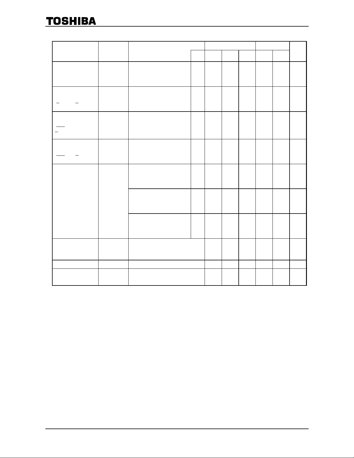
AC Characteristics (C
Characteristics Symbol
Output transition time
Propagation delay
time
, B-Q, Q)
(
A
Propagation delay
time
(
CLR TRIGGER-Q,
Q)
Propagation delay
time
CLR -Q, Q)
(
Output pulse width tw
Output pulse width
error between circuits
(in same package )
Input capacitance CIN ⎯ ⎯ 5 10 ⎯ 10 pF
Power dissipation
capacitance
= 50 pF, input: tr = tf = 6 ns)
L
Test Condition Ta = 25° C Ta = −40 to 85°C
t
∆tw
TLH
t
THL
t
pLH
t
pHL
t
pLH
t
pHL
t
pLH
t
pHL
C
OUT
OUT
PD
(Note)
Cx = 28 pF
= 6 kΩ (V
Rx
Rx
= 2 kΩ (V
Cx = 0.01 µF
Rx
= 10 kΩ
Cx = 0.1 µF
Rx
= 10 kΩ
⎯
⎯
⎯
⎯
= 2 V)
CC
= 4.5 V, 6 V)
CC
95
19
16
265
53
45
295
59
50
200
40
34
500
425
130
115
115
1.2
1.1
1.1
Unit
ns
ns
ns
ns
ns
µs
ms
V
CC
Min Typ. Max Min Max
(V)
2.0
4.5
6.0
2.0
4.5
6.0
2.0
4.5
6.0
2.0
4.5
6.0
2.0
4.5
6.0
2.0
4.5
6.0
2.0
0.9
4.5
0.9
6.0
0.9
⎯ ⎯ ±1 ⎯ ⎯ ⎯ %
⎯ ⎯ 162 ⎯ ⎯ ⎯ pF
⎯
⎯
⎯
⎯
⎯
⎯
⎯
⎯
⎯
⎯
⎯
⎯
⎯
⎯
⎯
90
95
95
30
102
29
22
102
31
23
68
20
16
700
250
210
110
105
105
1.0
1.0
1.0
75
⎯
15
13
42
36
47
40
32
27
⎯
⎯
⎯
⎯
⎯
⎯
⎯
⎯
⎯
⎯
⎯
⎯
⎯
⎯
90
95
95
0.9
0.9
0.9
2500
8
7
210
235
160
2000
400
340
130
115
115
1.2
1.1
1.1
Note: CPD is defined as the value of the internal equivalent capacitance which is c alculated from the operating
current consumption without load.
Average operating current can be obtained by the equation:
(opr) = C
I
CC
PD・VCC・fIN
+ ICC’・duty/100 + ICC/2 (per circuit)
(ICC’: active supply current)
(duty. %)
9
2006-06-01
Page 10

Output Pulse Width Constant K – Supply Voltage (typical)
t
– Cx Characteristics (typ.) trr – VCC Characteristics (typ.)
WOUT
TC74HC123AP/AF/AFN
10
2006-06-01
Page 11
Package Dimensions
TC74HC123AP/AF/AFN
Weight: 1.00 g (typ.)
11
2006-06-01
Page 12
Package Dimensions
TC74HC123AP/AF/AFN
Weight: 0.18 g (typ.)
12
2006-06-01
Page 13
Package Dimensions
TC74HC123AP/AF/AFN
Weight: 0.18 g (typ.)
13
2006-06-01
Page 14
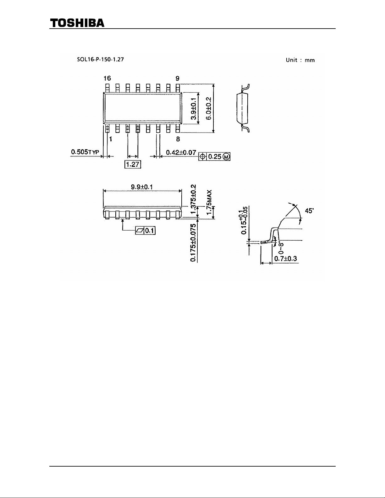
Package Dimensions (Note)
TC74HC123AP/AF/AFN
Note: Thi s pack age is not availabl e in Japan.
Weight: 0.13 g (typ.)
14
2006-06-01
Page 15
Note: Lead (Pb)-Free Packages
DIP16-P-300-2.54A SOP16-P-300-1.27A SOL16-P-150-1.27
TC74HC123AP/AF/AFN
RESTRICTIONS ON PRODUCT USE
• The information contained herein is subject to change without notic e. 021023_D
• TOSHIBA is continually working to improve the quality and reliability of its products. Nevertheless, semiconductor
devices in general can malfunction or fail due to their inherent electrical sensitivity and vulnerability to physical
stress. It is the responsibility of the buyer, when utilizing TOSHIBA products, to comply with the standards of
safety in making a safe design for the entire system, and to avoid situatio ns in which a malfunction or failure of
such TOSHIBA products could cause loss of human life, bodily injury or damage to propert y.
In developing your designs , please ensure t hat TOSHIBA products are used wit hin specifi ed operating ranges as
set forth in the most recent TOSHIBA products specifications. Also, please keep in mind the precautions and
conditions set forth in the “Handling Guide for Semiconductor Devices,” or “TOSHIBA Semiconductor Reliability
Handbook” etc.
• The TOSHIBA products listed in this document are intended for usage in general electronics applications
(computer, personal equipment, office equipment, measuring equipment, indust rial robotics , domestic applianc es,
etc.). These TOSHIBA products are neither intended nor warranted for usage in equipment that requires
extraordinarily high quality and/or reliability or a malfunction or failure of which may cause loss of human life or
bodily injury (“Unintended Usage”). Unintended Usage include atomic energy control instruments, airplane or
spaceship instruments, transportation instruments, traffic signal instruments, combustion control instruments,
medical instruments, all types of safety devices, etc. Unintended Usage of TOSHIBA products listed in this
document shall be made at the customer’s own risk.
• The products desc ribed in this document shall not b e used or embedded to any downstream products of which
manufacture, use and/or sale are prohibited under any applicable law s and regulations.
• The information contained herein is presented only as a guide for the applications of our products. No
responsibility is assumed by TOSHIBA for any infringements of patents or other rights of the third parties which
may res ult from its use. No l icense is granted by implic ation or ot herwis e under any patent or patent ri ghts of
TOSHIBA or others.
021023_A
021023_B
060106_Q
021023_C
060116EBA
• The products described in this document are subject to the forei gn exchang e and for eign tr ade laws . 021023_E
15
2006-06-01
 Loading...