

Page 1

October 1987
Revised March 2002
CD4017BC • CD4022BC
Decade Counter/Divider with 10 Decoded Outputs •
Divide-by-8 Counter/Divider with 8 Decoded Outputs
CD4017BC • CD4022BC Decade Counter/Divider with 10 Decoded Outputs • Divide-by-8 Counter/Divider with 8
Decoded Outputs
General Description
The CD4017BC is a 5 -sta ge divi d e- by-1 0 John son co unt er
with 10 decoded outputs and a carry out bit.
The CD4022BC is a 4- stage divide-by-8 Johnso n counter
with 8 decoded outputs and a carry-out bit.
These counters are clea red to t heir zero cou nt by a lo gical
“1” on their reset line. These counters are advanced on the
positive edge of the clock signal when the clock enable signal is in the logical “0” state.
The configuration of the CD4017BC and CD4022BC permits medium speed operatio n and assures a hazard free
counting sequence. The 10/8 decoded outputs are normally in the logical “0” st ate and go to the l ogical “1” state
only at their respective time slot. Each decoded output
remains high for 1 full clock cycle. The carry-out signal
completes a full cycle for every 10/8 clo ck inp ut cy cles a nd
is used as a ripple carry signal to any succeeding stages.
Features
■ Wide supply voltage range: 3.0V to 15V
■ High noise immunity: 0.45 V
■ Low power Fan out of 2 driving 74L
TTL compatibility: or 1 driving 74LS
■ Medium speed operation: 5.0 MHz (typ.)
with 10V V
■ Low power: 10 µW (typ.)
■ Fully static operation
DD
DD
(typ.)
Applications
• Automotive
• Instrumentation
• Medical electronics
• Alarm systems
• Industrial electronics
• Remote metering
Ordering Code:
Order Number Package Number Package Description
CD4017BCM M16A 16-Lead Small Outline Integrated Circuit (SOIC), JEDEC MS-012, 0.150" Narrow
CD4017BCSJ M16D 16-Lead Small Outline Package (SOP), EIAJ TYPE II, 5.3mm Wide
CD4017BCN N16E 16-Lead Plastic Dual-In-Line Package (PDIP), JEDEC MS-001, 0.300" Wide
CD4022BCM M16A 16-Lead Small Outline Integrated Circuit (SOIC), JEDEC MS-012, 0.150" Narrow
CD4022BCN N16E 16-Lead Plastic Dual-In-Line Package (PDIP), JEDEC MS-001, 0.300" Wide
Devices also availab l e in Tape and Reel. Specify by appending th e s uffix let t er “X” to the ordering code.
Connection Diagrams
Pin Assignments for DIP, SOIC and SOP
CD4017B
Top View
© 2002 Fairchild Semiconductor Corporation DS005950 www.fairchildsemi.com
Pin Assignments for DIP and SOIC
CD4022B
Top View
Page 2
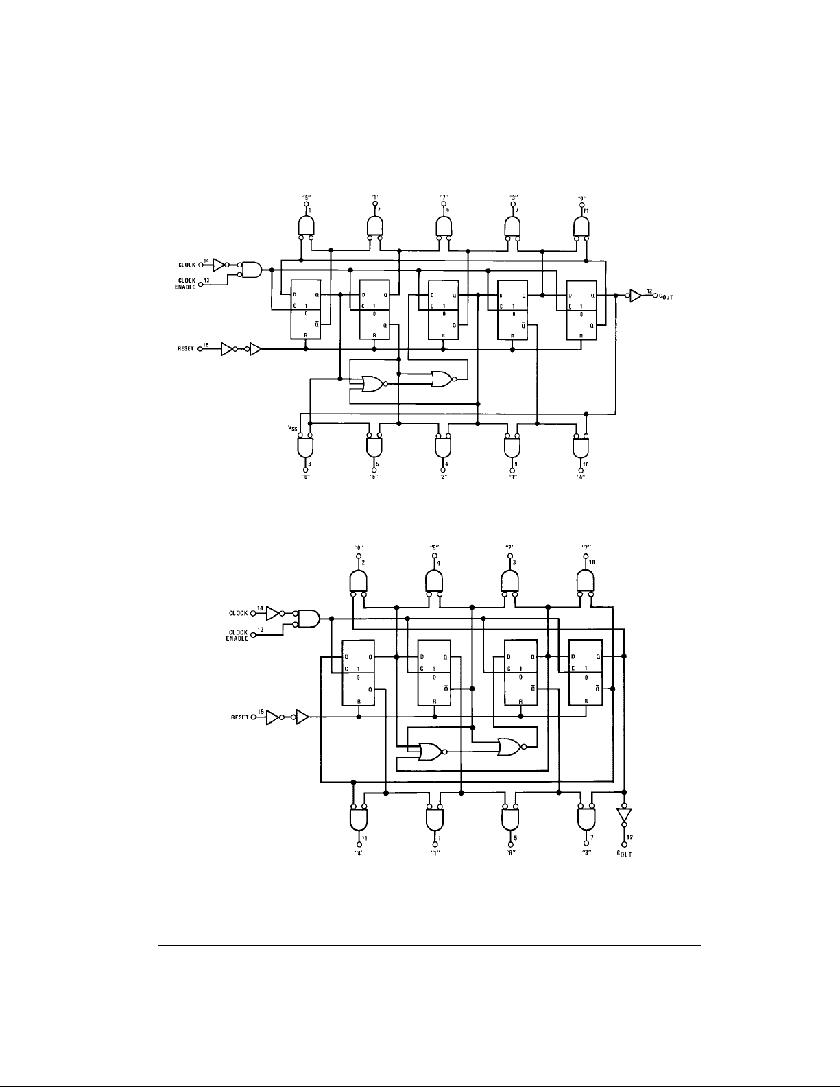
Logic Diagrams
CD4017BC • CD4022BC
Ter minal N o . 8 = GND
Ter minal N o . 16 = V
DD
CD4017B
CD4022B
Ter minal N o . 16 = V
Ter minal N o . 8 = GND
DD
www.fairchildsemi.com 2
Page 3
Absolute Maximum Ratings(Note 1)
(Note 2)
DC Supply Voltage (VDD) −0.5 VDC to +18 V
Input Voltage (VIN) −0.5 VDC to VDD +0.5 V
Storage Temperature (TS) −65°C to +150°C
Power Dissipation (P
Dual-In-Line 700 mW
Small Outline 500 mW
Lead Temperature (T
(Soldering, 10 seconds) 260
)
D
)
L
Recommended Operating
Conditions
DC Supply Voltage (V
DC
Input Voltage (VIN) 0 to VDD V
DC
Operating Temperature Range (TA) −55°C to +125°C
Note 1: “Absolute Maximum Ratings” are those values bey ond which the
safety of the device ca nnot be guaranteed, they are not meant to imply that
the devices should be operated at these limits. The table of “Recom-
mended Operating Conditions” and “Electrical Characteristics” provides
conditions for actual device operation.
= 0V unless otherw is e s pecified.
Note 2: V
°C
SS
(Note 2)
) +3 VDC to +15 V
DD
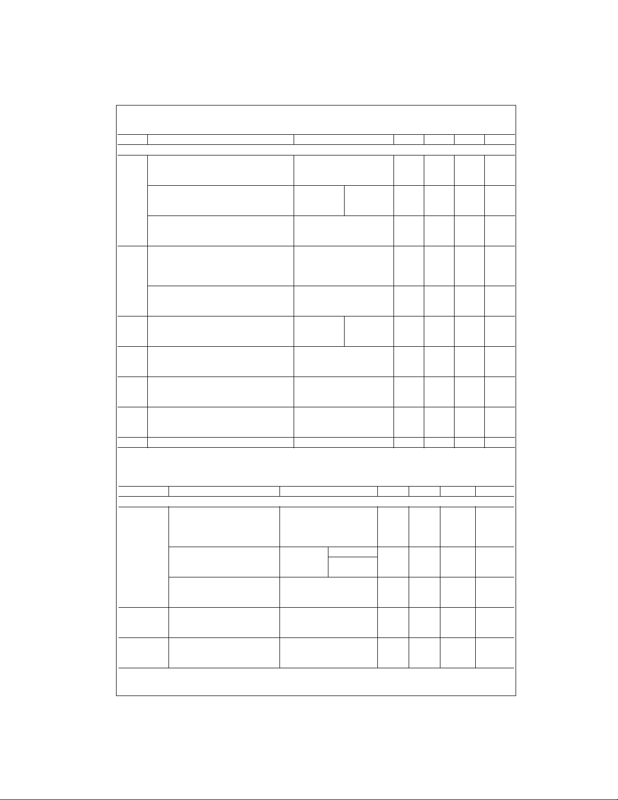
DC Electrical Characteristics (Note 2)
Symbol Parameter Conditions
I
Quiescent Device VDD = 5V 5 0.3 5 150
DD
V
LOW Level |IO| < 1.0 µA
OL
Output Voltage VDD = 5V 0.05 0 0.05 0.05
V
HIGH Level |IO| < 1.0 µA
OH
Output Voltage V
LOW Level |IO| < 1.0 µA
V
IL
Input Voltage VDD = 5V, VO = 0.5V or 4.5V 1.5 1.5 1.5
V
HIGH Level |IO| < 1.0 µA
IH
Input Voltage V
I
LOW Level Output VDD = 5V, VO = 0.4V 0.64 0.51 0.88 0.36
OL
I
HIGH Level Output VDD = 5V, VO = 4.6V −0.25 −0.2 −0.36 −0.14
OH
I
Input Current VDD = 15V, VIN = 0V −0.1 −10−5−0.1 −1.0
IN
Note 3: IOL and IOH are tested one output at a ti m e.
= 10V 10 0.5 10 300
DD
VDD = 15V 20 1.0 20 600
VDD = 15V 0.05 0 0.05 0.05
= 5V 4.95 4.95 5 4.95
DD
V
= 15V 14.95 14.95 15 14.95
DD
= 10V, VO = 1.0V or 9.0V 3.0 3.0 3.0
DD
= 15V, VO = 1.5V or 13.5V 4.0 4.0 4.0
V
DD
= 5V, VO = 0.5V or 4.5V 3.5 3.5 3.5
DD
= 10V, VO = 1.0V or 9.0V 7.0 7.0 7.0
DD
V
= 15V, VO = 1.5V or 13.5V 11.0 11.0 11.0
DD
= 10V, VO = 0.5V 1.6 1.3 2.25 0.9
DD
V
= 15V, VO = 1.5V 4.2 3.4 8.8 2.4
DD
= 10V, VO = 9.5V −0.62 −0.5 −0.9 −0.35
DD
VDD = 15V, VO = 13.5V −1.8 −1.5 −3.5 −1.1
VDD = 15V, VIN = 15V 0.1 10−50.1 1.0
−55°C +25°+125°C
Min Max Min Typ Max Min Max
CD4017BC • CD4022BC
DC
DC
Units
µACurrent V
VVDD = 10V 0.05 0 0.05 0.05
VVDD = 10V 9.95 9.95 10 9.95
VV
VV
mAC ur rent (Note 3) V
mAC ur rent (Note 3) V
µA
3 www.fairchildsemi.com
Page 4
AC Electrical Characteristics (Note 4)
T
= 25°C, CL= 50 pF, RL= 200k, t
A
Symbol Parameter Conditions Min Typ Max Units
CLOCK OPERATION
t
Propagation Delay Time Carry Out Line VDD = 5V 415 800
PHL, tPLH
Carry Out Line VDD = 5V
CD4017BC • CD4022BC
Decode Out Lines VDD = 5V 500 1000
t
, t
Transition Time Carry Out and Decode Out Lines
TLH
THL
t
TLH
t
THL
f
Maximum Clock Frequency VDD = 5V Measured with 1.0 2
CL
tWL, tWHMinimum Clock Pulse Width VDD = 5V 125 250
t
, t
Clock Rise and Fall Time VDD = 5V 20
rCL
fCL
t
Minimum Clock Inhibit Data Setup Time VDD = 5V 120 240
SU
C
Average Input Capacitance 57.5pF
IN
Note 4: AC Parameters are gu aranteed by DC correlated testing.
rCL
and t
= 20 ns, unless otherwise specified
fCL
= 10V 160 320
DD
= 15V 130 250
V
DD
240 480
C
= 15 pF
= 15V 70 140
V
DD
= 10V 200 400
DD
= 15V 160 320
V
DD
L
VDD = 5V 200 360
= 10V 100 180
DD
VDD = 15V 80 130
VDD = 5V 100 200
VDD = 15V 40 80
VDD = 15V Output Line 3.0 6
VDD = 15V 35 70
VDD = 15V 5
VDD = 15V 32 65
nsV
nsVDD = 10V 85 170
nsV
nsV
nsVDD = 10V 50 100
MHzVDD = 10V Respect to Carry 2.5 5
nsVDD = 10V 45 90
µsVDD = 10V 15
nsVDD = 10V 40 80
AC Electrical Characteristics (Note 4)
T
= 25°C, CL = 50 pF, RL = 200k, t
A
Symbol Parameter Conditions Min Typ Max Units
RESET OPERATION
t
PHL, tPLH
Propagation Delay Time
Carry Out Line VDD = 5V 415 800
Carry Out Line VDD = 5V 240 480
Decode Out Lines VDD = 5V 500 1000
t
W
t
REM
Minimum Reset VDD = 5V 200 400
Minimum Reset VDD = 5V 75 150
www.fairchildsemi.com 4
rCL
and t
= 20 ns, unless otherwise specified
fCL
VDD = 15V 130 250
VDD = 15V 70 140
VDD = 15V 160 320
VDD = 15V 55 110
VDD = 15V 25 50
nsVDD = 10V 160 320
nsVDD = 10V CL = 15 pF 85 170
nsVDD = 10V 200 400
nsPulse Width VDD = 10V 70 140
nsRemoval Time VDD = 10V 30 60
Page 5
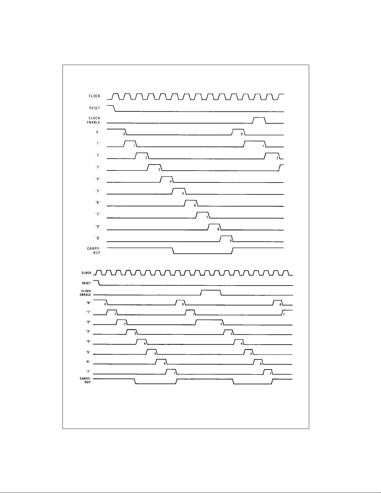
Timing Diagrams
CD4017BC • CD4022BC
CD4017B
CD4022B
5 www.fairchildsemi.com
Page 6
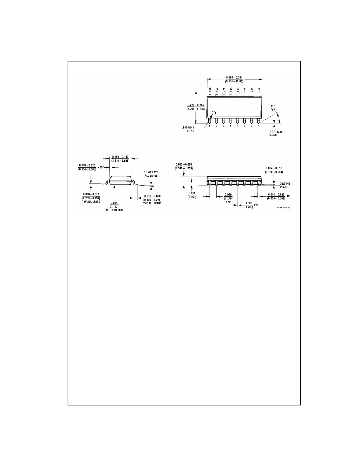
Physical Dimensions inches (millimeters) unless otherwise noted
CD4017BC • CD4022BC
16-Lead Small Outline Integrated Circuit (SOIC), JEDEC MS-012, 0.150" Narrow
Package Number M16A
www.fairchildsemi.com 6
Page 7
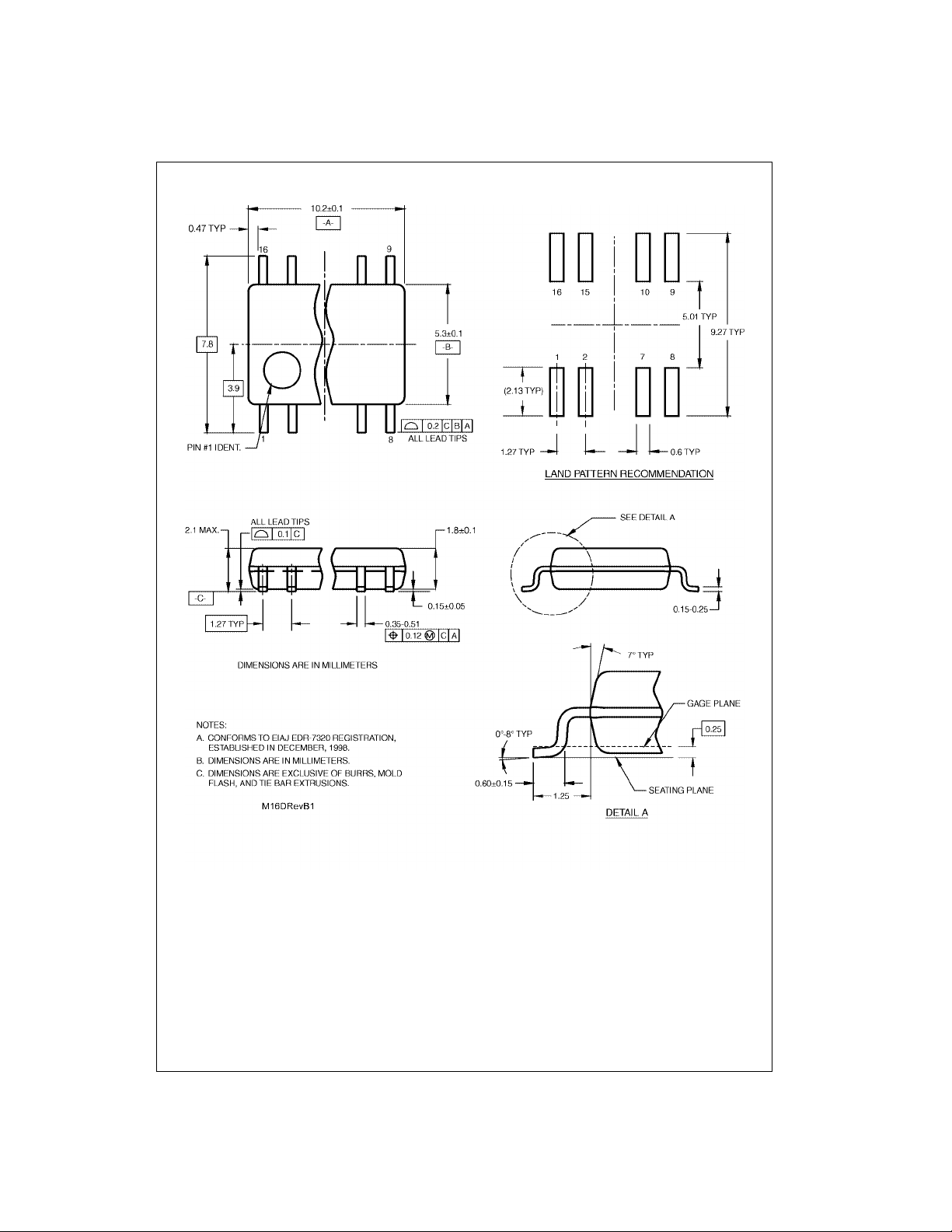
Physical Dimensions inches (millimeters) unless otherwise noted (Continued)
CD4017BC • CD4022BC
16-Lead Small Outline Package (SOP), EIAJ TYPE II, 5.3mm Wide
Package Number M16D
7 www.fairchildsemi.com
Page 8
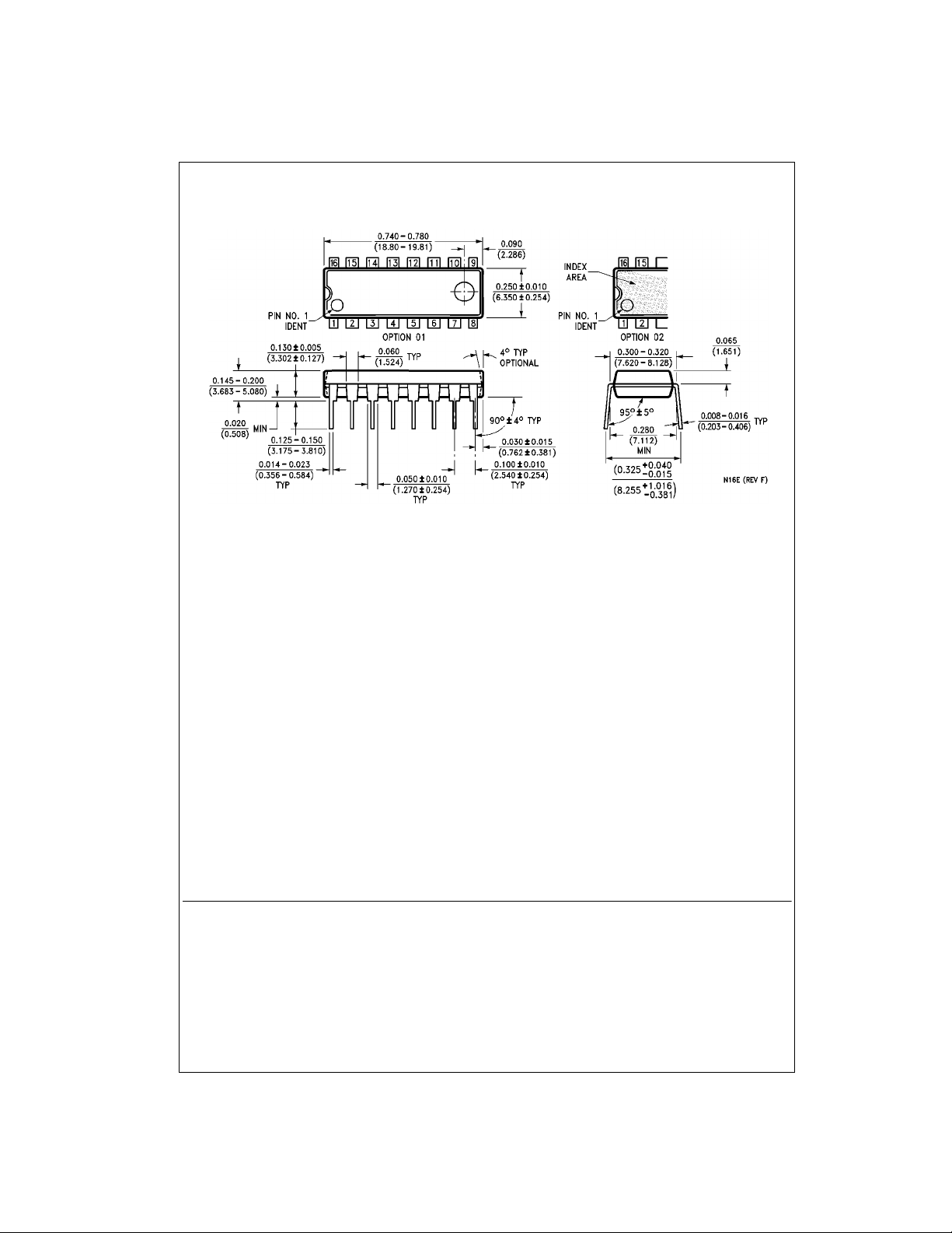
Physical Dimensions inches (millimeters) unless otherwise noted (Continued)
Decoded Outputs
16-Lead Plastic Dual-In-Line Package (PDIP), JEDEC MS-001, 0.300" Wide
Fairchild does not assume any responsibility for use of any circuitr y described, no circuit patent licenses are implied a nd
Fairchild reserves the right at any time without notice to change said circuitry and specifications.
LIFE SUPPORT POLICY
FAIRCHILD’S PRODUCTS ARE NOT AUTHORIZED FOR USE AS CRITICAL COMPONENTS IN LIFE SUPPORT
DEVICES OR SYSTEMS WITHOUT THE EXPRESS WRITTEN APPROVAL OF THE PRESIDENT OF FAIRCHILD
SEMICONDUCTOR CORPORATION. As used herein:
1. Life support devices or systems are device s or syste ms
which, (a) are intended for surgical implant into the
body, or (b) support or sustain life, and (c) whose failure
to perform when properly used in accordance with
instructions for use provided in the labeling, can be rea-
CD4017BC • CD4022BC Decade Counter/Divider with 10 Decoded Outputs • Divide-by-8 Counter/Divider with 8
sonably expected to result in a significant inju ry to the
user.
Package Number N16E
2. A critical component in any compon ent of a l ife supp ort
device or system whose failu re to perform can be reasonably expected to cause the failure of the li fe su pp ort
device or system, or to affect its safety or effectiveness.
www.fairchildsemi.com
www.fairchildsemi.com 8
 Loading...