

Page 1
SUMMIT
MICROELECTRONICS, Inc.
SMD1108
8-Channel Auto-MonitorTM ADC
In System Programmable Analog (ISPA
FEATURES
!!
! Programmable 8 Channel 10-Bit A to D con-
!!
verter
""
" Programmable Sequencing of Analog
""
Switches in Auto-Monitor Mode
""
" Resolution of 10 bits
""
""
" Differential Non-Linearity of ±1LSB
""
""
" Top 4 Channels Programmable, Nonvolatile
""
Upper/Lower IRQ Limits
""
" Bottom 4 Channels Tied to Matching Pro-
""
grammable, Nonvolatile Comparators
""
" 4 Companion Over-current Comparators
""
!!
! Internal Temperature Sensor
!!
Preliminary
TM
) Device
!!
!
Programmable LED Driver Outputs
!!
!!
!
Programmable, Nonvolatile Combinatorial Reset
!!
logic
!!
!
Nonvolatile Status Capture Register
!!
!!
! Two Programmable, Nonvolatile Watchdog
!!
Timers
!!
! 1K-Bit Nonvolatile Memory
!!
!!
! Industry Standard 2-Wire Interface
!!
""
" Nonvolatile Configuration Registers
""
""
" ADC Conversion Results
""
""
" Memory Array
""
""
" Mechanism for System Level Presence Detect
""
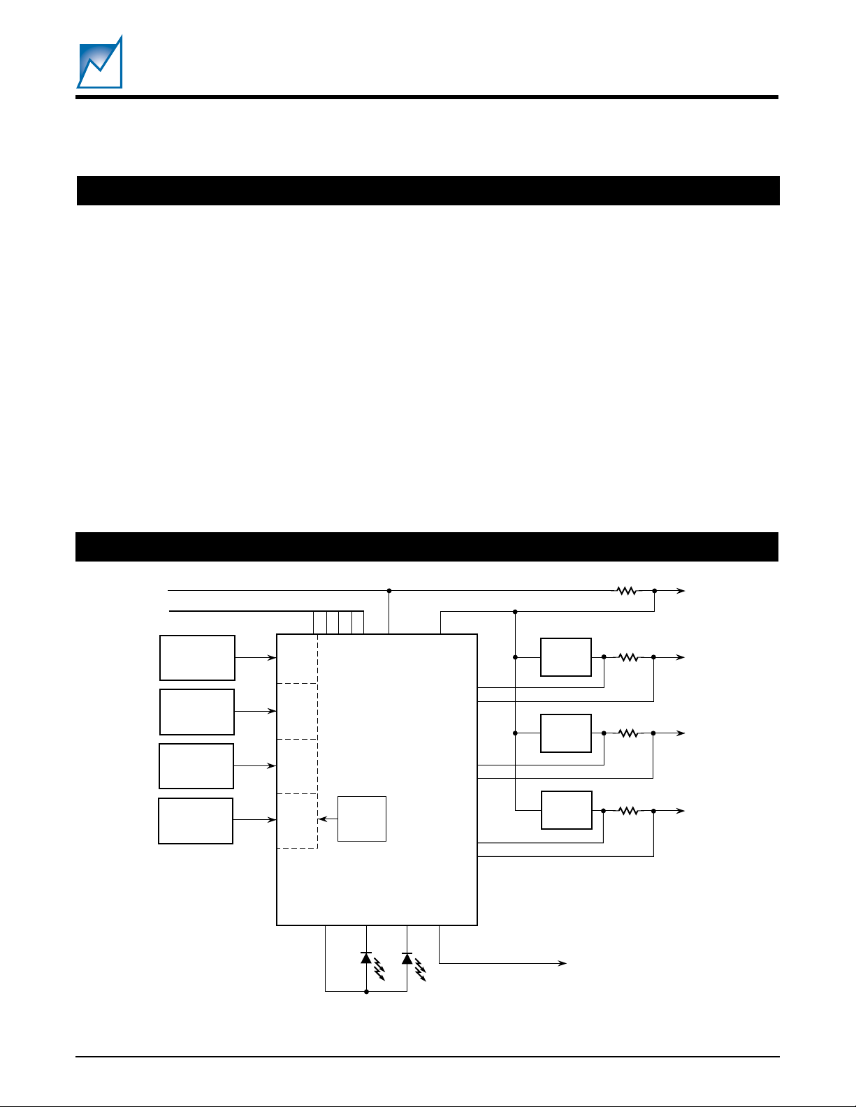
SIMPLIFIED APPLICATION DRAWING
5V
2
I
C
EXT. TEMP .
SENSOR
CURRENT
SENSOR
CH0
CH1
SMD1108
AIRFLOW
SENSOR
ENVIRON-
MENTAL
MONITOR
CH2
CH3
Internal
Temp.
Sensor
AUXVCC
SMBALERT
/CH4
CC0
V
RDY#
V
V
V
CC1
CC2
CC3
OC0
/CH5
OC1
/CH6
OC2
/CH7
OC3
RST#
OC0OC0OC0OC0
LDO
LDO
LDO
5V
3.3V
2.5V
1.8V
RESET#
2052 SAD
©SUMMIT MICROELECTRONICS, Inc., 2001 • 300 Orchard City Dr., Suite 131 • Campbell, CA 95008 • Phone 408-378-6461 • FAX 408-378-6586 • www.summitmicro.com
Characteristics subject to change without notice
2052 2.0 10/05/01
1
Page 2
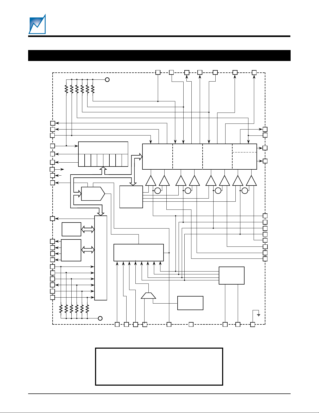
FUNCTIONAL BLOCK DIAGRAM
SMD1108
Preliminary
DLYD_RST#
RST#
MR#
AUTOMON
LIM_IRQ#
SMB
ALERT
V
REFIN
V
REFOUT
RDY#
AUXV
GPO-0
GPO-1
GPO-2
GPO-3
A0
A1
A2
SDA
SCL
CE#
OV_IRQ#
12
13
V
CC
All Resistors
are 100k
Ω
WD_EN# LDO#
WLDI
WDO#
48
3
1
2
IRQ_RST#
7
OC_IRQ#
14
15
5
9
11
4
Programmable Combi-
natorial Logic
Hi
Hi
Lo
0
0
Hi
Lo
1
2
1
Lo
Nonvolatile
Programmable
Hi
Lo
3
3
2
Combinatorial
Reset Logic
Reset Timer
Nonvolatile
Programmable
Watchdog
Timer
Logic
Programmable
Combinatorial
Interrupt
Logic
Nonvolatile
Status
Register
23
HEALTHY#
UV_OVRD
16
24
FAULT#
10
FAULT_IRQ#
29
20
6
10-Bit
ADC
42
CC
Memory
Array
28
27
26
25
43
44
Four
General
Purpose
Outputs
Serial Interface
Reference
Select
& Trim
Logic
Programmable
NV-OU
Octal Analog
Switch
–
+
50
mV
45
NV-OU
–
+
–
+
50
mV
NV-OU
–
+
–
+
+
50
mV
Control &
Distribution
NV-OU
–
Power
–
–
+
+
50
mV
41
V
/CH4
CC0
40
V
/CH5
CC1
39
V
/CH6
CC2
38
/CH7
V
CC3
34
OC3
35
OC2
36
OC1
37
OC0
46
47
22
All Resistors
are 100k
Ω
Temperature
Sensor
V
CC
33
CH0
32
CH1
31
CH2
30
CH3
19
AGND
21
Reserved
17
PGND
18
DGND
8
GND
2052 BD 1.1
RECOMMENDED OPERATING CONDITIONS
Temperature –40ºC to 85ºC.
Voltage 2.7V to 5.5V
2
2052 2.0 10/05/01
SUMMIT MICROELECTRONICS, Inc.
Page 3
INTRODUCTION
SMD1108
Preliminary
The SMD1108 is a versatile, programmable 8-channel,
10-bit Data Acquisition System that is designed to operate
autonomously, relieving the system host and logic board
of the environmental monitoring tasks.
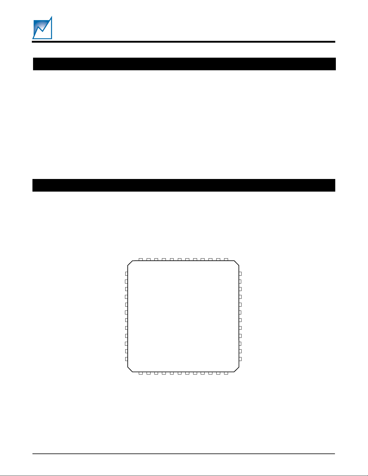
PIN CONFIGURATION
48-Pin TQFP
WLDI
SCL
SDAA2A1A0AUXV
Programming of configuration, control and calibration
values by the user can be simplified with the interface
adapter and Windows GUI software obtainable from
Summit Microelectronics.
CC
/CH4
/CH5
/CH6
/CH7
CC0
CC1
CC2
V
CC3
V
V
V
OC0
LDO#
WDO#
WD_EN#
SMB
ALERT
MR#
RDY#
IRQ_RST#
GND
AUTOMON
FAULT_IRQ#
LIM_IRQ#
OC_IRQ#
4847464544434241403938
1
2
3
4
5
6
7
8
9
10
11
12
1314151617181920212223
RST#
PGND
DGND
AGND
OV_IRQ#
UV_OVRD
V
DLYD_RST#
CE#
REFOUT
Reserved
37
OC1
36
OC2
35
34
OC3
CH0
33
CH1
32
CH2
31
CH3
30
V
29
GPO-0
28
GPO-1
27
GPO-2
26
GPO-3
25
24
FAUALT#
2052 PCon 1.0
HEALTHY#
REFIN
SUMMIT MICROELECTRONICS, Inc.
2052 2.0 10/05/01
3
Page 4
ABSOLUTE MAXIMUM RATINGS
SMD1108
Preliminary
Temperature Under Bias ...................... –55°C to 125°C
Storage Temperature ........................... –65°C to 150°C
Lead Solder Temperature (10s) ......................... 300 °C
Output Short Circuit Current ........................ # 100mA
Terminal Voltage with Respect to GND (AGND,
DGND & PGND tied):
Digital Inputs:IRQ_RST#, WD_EN#, MR#, WLDI, SCL,
Digital Outputs: ................. LDO#, WDO#, SMB
HEALTHY#, FAULT_IRQ#, LIM_IRQ#,
OC_IRQ#, RST#, OV_IRQ#, DLYD_RST#,
FAULT#, RDY#, GPO-0, GPO-1, GPO-2, and
GPO-3 ............................................. –2V to 7V
Analog Inputs: V
V
CC3
CC0
/CH7, CH0, CH1, CH2, CH3, OC1, OC2,
OC3, AUXVCC, and V
CE#, A0, A1, A2, and AUTOMON .... –2V to 7V
#
Output shorted for no more than one second, no more
than one output shorted at a time.
DC OPERATING CHARACTERISTICS
(Over Recommended Operating Conditions; Voltages are relative to GND)
lobmySretemaraPsnoitidnoC )1etoN( .niM.pyT.xaMstinU
I
CC
I
BS
I
IL
I
OL
V
1LO
V
2LO
V
HO
V
LI
V
HI
tuOtnerrucegakaeltupV
stupnIgolanA
V
V
V
V
I
Note 1: Unless otherwise specified VCC is the highest of the four V
V
NIFER
1NI
2NI
3NI
ORV
FER
hguorhtVCC3HC/3
V
TUOFER
tnerruCylppuSnepostuptuollA13Am
tnerruCybdnatS
tnerrucegakaeltupnIV
egatlovwoltuptuO
egatlovwoltuptuO
egatlovhgihtuptuO
NI
TUO
I
LO
I
LO
V
CC
V
CC
V
CC
V
CC
VotV0=
CC
VotV0=
CC
Am5=4.0
Am1=4.0
I,V5=
LO
I,V5.4<
LO
I,V5=
LO
I,V5.4<
LO
,eldiCDA,nepostuptuollA
ssecorpniyromemon
Am1.2=4.0
Am1=2.0
Am004–= 4.2
Am001–=V
CC
egatlovwoltupnI1.0– 3.0 × V
egatlovhgihtupnI2V
egatlovtupni15V
VnoegatlovtupnI
7hguorht
3COhguorht
tnerruc
0HC/0
CC
4slennahcnoegatlovtupnI
0COnoegatlovtupnI
V
TUOFER
V
TUOFER
V5.2=1
V840.2=1
/CHX inputs.
CCX
05.5V
02× V
0V
/CH4, V
2.0–
ALERT
/CH5, V
CC1
IN .............. –2V to 7V
REF
CC2
/CH6,
1.01Am
2Aµ
01Aµ
CC
1+V
CC
NIFER
CC
2052 Elect Table 1.0
#,
V
V
V
V
V
V
Am
4
2052 2.0 10/05/01
SUMMIT MICROELECTRONICS, Inc.
Page 5

PIN DESCRIPTIONS
V
/CH4 – V
CC0
These 4 inputs are used as the voltage monitor inputs and
the voltage supply for the SMD1108. Internally they are
diode ORed and the input with the highest voltage potential will be the default supply voltage. For proper device
operation at least one of the inputs must be at 2.7V or
higher. V
CC0
programmable comparators. The under-voltage and
over-voltage threshold voltage of each comparator is
programmable.
V
(29)
REFIN
A reference voltage for the ADC. The user can select
either the VREFIN as the ADC reference or use the default
internal reference voltage.
V
REFOUT
(20)
The internally generated reference voltage. It is programmable and can supply either 2.048V or 2.500V.
AGND, DGND, PGND, GND (19, 18, 17, 8)
These are the analog, digital, package, and common
ground inputs, respectively. They should all be tied to the
same ground plane.
/CH7 (38, 39, 40, 41)
CC3
/CH4 to V
/CH7 are also inputs to four
CC3
SMD1108
Preliminary
SDA (46)
Serial data input/output pin. It should be tied to V
through a 10kΩ pull-up resistor.
SCL (47)
Serial clock input pin. It should be tied to VCC through a
10kΩ pull-up resistor.
CH0 to CH3 (33, 32, 31, 30)
The analog channel inputs. These inputs are monitored
solely through the use of the ADC.
OC0 to OC3 (37, 36, 35, 34)
Over-current sense inputs. They are paired with VCC0/
CH4 to VCC3/CH7, respectively, and have a fixed 50mV
offset with respect to their corresponding channel input.
MR# (5)
An active low manual reset input. When MR# is driven low
the reset output will immediately be driven low. MR# is not
maskable and will always generate a reset sequence. The
duration of the RST# pulse will be equal to the length of the
MR# input pulse plus the programmed reset time-out
period value.
CC
AUXVCC (42)
AUXVCC should be isolated from the system power
supplies and tied to ground through capacitor C
normal device operation C
will be charged by the
B/U
. During
B/U
system supplies through the SMD1108. If system power
is lost the charge on C
will be used to store the status
B/U
of the monitor inputs. A 10µF tantalum capacitor should
be used for C
B/U
.
In the system environment AUXVcc could also be connected to the front of the card (along with SDA and SCL
and GND) so that power could be applied to the SMD1108
to read the contents of the NV status registers.
A0, A1 and A2 (43, 44, 45)
Address inputs. When addressing the SMD1108 either as
a memory or an analog channel (or configuration register)
the address inputs distinguish which one of eight possible
devices sharing the common bus is being addressed.
CE# (22)
A control mechanism for the 2-wire interface. The true
state polarity is programmable. When driven true the
interface is active and communications channels are
open. When it is driven false all communications via the
bus are disabled.
WD_EN# (3)
The enable input for both the Watchdog and the Longdog.
It must be driven low to enable the operation of their
timers. This can provide a convenient mechanism during
“debug of code” or during a “power-on configuration”
sequence.
WLDI (48)
The Watchdog timer interrupt input. A low to high
transition on WDI will reset the Watchdog and Longdog
timers. If the timer is not reset within the programmed
period of time the SMD1108 will activate the WDO# output
first and then the LDO# output.
RST# (15)
An active low open drain output. It will be driven low by
the combination of VCC0/CH4 to VCC3/CH7 being at
levels below their programmed settings and/or MR# being
driven low. RST# will stay low for the duration of the fault
condition or the MR# low input and remain low for the
duration of t
after the removal of the fault condition
PURST
or MR# returning high.
SUMMIT MICROELECTRONICS, Inc.
2052 2.0 10/05/01
5
Page 6

SMD1108
Preliminary
DLYD_RESET# (14)
An active low open drain output. During normal system
operation it will be driven low by the combination of VCC0/
CH4 to VCC3/CH7 being at levels below their programmed settings. During the power-on sequence it will
be delayed to allow the system to power-up in a controlled
sequenced order. See Table 19 for the delay values.
SMB
ALERT
# (4)
An active low open drain output. It will be driven low
whenever one or more of the four auto-monitor inputs
exceeds its limits. Once the SMB
# output is driven
ALERT
low the SMD1108 will respond to the industry standard
SMB protocol and identify itself as the generator of the
alert.
LIM_IRQ# (11)
An active low open drain output that is programmable to be
driven low whenever any one of the selected auto-monitor
inputs exceeds the programmed high or low value.
FAULT# (24)
An open drain output that can be programmed to drive the
output low whenever a selected source is out of limits
(FAULT#). Conversely it can be programmed to drive the
output low (FAULT) whenever the selected sources are
within limits.
HEALTHY# (23)
An open drain output that can be programmed to drive the
output low whenever a selected source is out of limits
(HEALTHY). Conversely it can be programmed to drive
the output low whenever the selected sources are within
limits (HEALTHY#).
WDO# (2)
Watchdog Timer Output is an active low open drain output
that can be wire-ORed with any number of open drain
outputs. Whenever the programmed time-out period of
the Watchdog timer is exceeded this output will be driven
low.
RDY# (6)
An active low status output indicating the ADC has no
conversion ongoing and the SMD1108 can be accessed
via the serial interface without risk of disturbing a conversion.
GPO-0 to GPO-3 (28, 27, 26, 25)
General purpose outputs that can be accessed via the
two-wire serial interface. The register controlling these
outputs is located in the GFS register section. The GPx
outputs are open drain and will be active when a “1” is
written to the corresponding bit position in GFS Register
0x98. The SMD1108 will power-up with the GPx bits
cleared; therefore, the outputs will not be actively driven.
AUTOMON (9)
This input must be high to enable the Auto Monitor
function.
OV_IRQ# (13)
This is an active low open drain output that is driven low
when the selected over-voltage conditions are true.
OC_IRQ# (12)
This is an active low open drain output that is driven low
when the selected over-current conditions are true.
IRQ_RST# (7)
The IRQ# outputs are latched. Strobing this signal low will
reset the IRQ# outputs. They can also be cleared by
accessing Register 99 (see Table 29).
UV_OVRD (16)
Forcing this input high will disable Under-Voltage reset
conditions.
FAULT_IRQ# (10)
This is an active low open drain output that is driven low
when the selected fault conditions are true.
LDO# (1)
Longdog Timer Output is an active low open drain output
that can be wire-ORed with any number of open drain
outputs. Whenever the programmed time-out period of
the Longdog timer is exceeded this output will be driven
low.
6
2052 2.0 10/05/01
SUMMIT MICROELECTRONICS, Inc.
Page 7

DEVICE OPERATION
SMD1108
Preliminary
THE ADC AND THE ANALOG SWITCH
10-bit ADC
The 10-bit ADC is a self-clocking SAR implementation. In
the manual mode of conversion the sample and hold
operation will begin after the SMD1108 has received the
request for conversion and the channel address. See
Table 1.
8 Analog Channels
The eight analog channels can be separated into two
function blocks: the bottom four channels (V
V
/CH7) are primarily supply voltage monitors; the top
CC3
CC0
/CH4 to
four channels (CH0 to CH3) are primarily environmental
monitors. All eight channels can be switched to the 10-bit
ADC and have their inputs converted on-command. CH0
to CH3 may be placed in the Auto-Monitor mode.
V
/CH4 to V
CC0
/CH7 provide four inputs to the analog
CC3
switch that controls the analog inputs to the ADC converter. Although these channels cannot be placed in the
Auto-Monitor mode, the host can request a direct conversion.
Because these channels are designed to operate as
supply voltage monitors they are each tied into a programmable comparator. The comparator threshold voltage is
programmable and the polarity of the threshold is programmable. This allows very precise monitoring of underor over-voltage conditions. Paired with each of these
.Cº52@oitaresioNotlangiS.nomBd07
DHT.nimBd08–
cinomrahkaeP
redrodn2.nimBd08–
noitaludomretni
noitrotsid
redrodr3.nimBd08–
52@emitnoisrevnoC º .C.monsµ08
ycaruccACD
noituloseRstib01
gnissimonhcihwrofnoitulosermuminiM
deetnaraugerasedoc
stib01
ycaruccaevitaleRBSL½±
LNDBSL1±
rorreelacsllufevitisoPBSL2±
V
rorretesfforalopnU
V
V5=
CC
CC
CC
V6.3otV7.2=
V7.2otV8.1=
BSL2±V
2052 Table01
Table 1. Typical ADC Performance
channels is an over-current input (OC0 to OC3) that is
offset from its partner comparator by 50mV.
TIMER FUNCTIONS
WATCHDOG and LONGDOG
The SMD1108 has two programmable Watchdog timers
each with its own output (WDO# and LDO#) and a common reset input (WLDI). Both are independently programmable and both can be placed in an idle mode. See
Register 8C.
RST#
This reset output is intended to be used to drive the
backend logic. It is an active low open drain output that is
driven low whenever V
CC0
, V
CC1
, V
CC2
or V
is below its
CC3
programmed threshold and/or MR# is being driven low. It
will stay low for the duration of the fault condition or the
MR# low input and remain low for the duration of t
PURST
(the programmed reset pulse width) after removal of the
fault condition or MR# returning high. It will also be driven
low whenever an over-current condition is detected. See
Register 8C.
DLYD_RST#
This output is activated by the same set of conditions as
RST#. However, during a power-up operation it will not be
immediately asserted. As soon as power to one of the
V
/CH4 to V
CC0
/CH7 inputs is detected a time-out
CC3
sequence will be started. The time-out period is programmable and should be equal to or greater than the worst
case power-on skew between all the supplies being monitored. If all of the supplies have not reached their threshold
before the time-out period, DLYD_RST# will be asserted.
DLYD_RST# can then be used to disable a voltage
sequencer such as the SMH4803A or SMH4804. See
Register 8D.
OUTPUTS
FAULT and HEALTHY
Two programmable outputs (active high or active low) that
will respond to programmed source activators. See Registers 8F and 90 through 95.
IRQs
The interrupt outputs are active low open drain outputs
that are driven low whenever one of the corresponding
monitor inputs senses an excursion beyond its programmed value. See Registers 88, 89, and 98 through 9F.
SUMMIT MICROELECTRONICS, Inc.
2052 2.0 10/05/01
7
Page 8
SMD1108
Preliminary
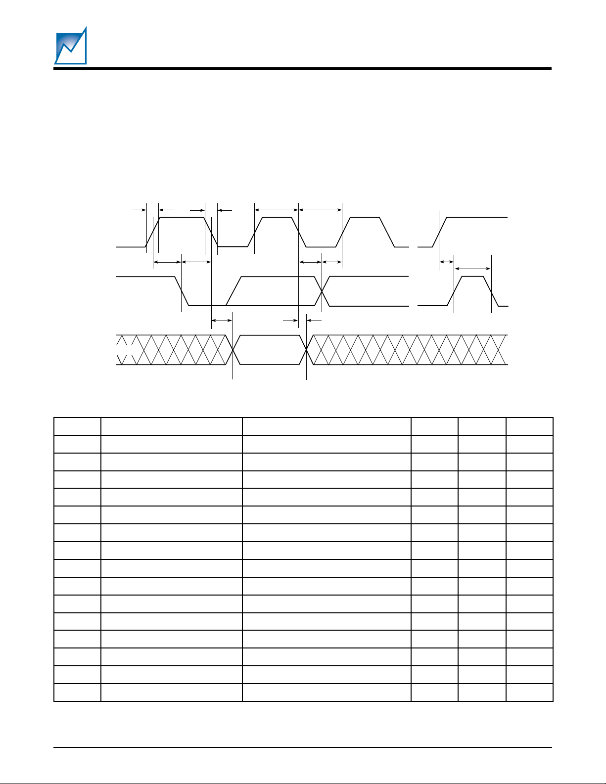
SERIAL INTERFACE
The SMD1108 has an industry standard 2-wire serial
interface. It supports four (4) device-type addresses:
1010 for reading and writing the memory array; 1001 for
reading and writing the nonvolatile limit registers and
t
t
SCL
t
SDA In
SDA Out
R
SU:SDA
t
F
t
HD:SDA
t
AA
HIGH
t
HD:DAT
Figure 1. Memory Timing
initiating ADC conversions; 1011 for access to the configuration registers, and 0001 that is used for responses to the
SMB
ALERT
protocol
In order to facilitate host system presence detection
techniques the SMD1108 provides A0, A1 and A2 address
inputs.
t
LOW
t
SU:DAT
t
DH
t
SU:STO
t
BUF
2052 Fig01 1.0
lobmySretemaraPsnoitidnoC.niM.xaMstinU
f
LCS
t
WOL
t
HGIH
t
FUB
t
ATS:US
t
ATS:DH
t
OTS:US
t
AA
t
HD
t
R
t
F
t
TAD:US
t
TAD:DH
ycneuqerfkcolcLCS 0001zHk
doirepwolkcolC 7.4sµ
doirephgihkcolC 0.4sµ
)1(emiteerfsuBnoissimsnartwenerofeB7.4sµ
emitputesnoitidnoctratS 7.4sµ
emitdlohnoitidnoctratS 0.4sµ
emitputesnoitidnocpotS 7.4sµ
tuptuodilavotegdekcolC)nelcyc(ADSdilavotwolLCS3.05.3sµ
)1(emitdlohtuOataDegnahcADSot)1+nelcyc(wolLCS3.0sµ
)1(emitesirADSdnaLCS 0001sn
)1(emitllafADSdnaLCS 003sn
)1(emitputesnIataD 052sn
)1(emitdlohnIataD 0sn
IT)1(ADSdnaLCSretlifesioNnoisserppusesioN001sn
t
RW
Note (1) These values are guaranteed by design.
emitelcycetirW 5sm
2052 Table02 1.0
Table 2. Memory Timing
8
2052 2.0 10/05/01
SUMMIT MICROELECTRONICS, Inc.
Page 9

MEMORY AND REGISTER OPERATION
SMD1108
Preliminary
The SMD1108 incorporates a memory that is configured
as a 128 x 8 array. Concatenated with the memory array
are the sixteen registers that hold the upper and lower
limits for ADC comparison tables. Additional registers
provide space for configuration usage. Another space is
provided for individual channel conversion initiations and
reading the conversion data.
All Read and Write operations to memory are handled via
an industry standard two-wire interface. The bus was
designed for two-way, two-line serial communication
between different integrated circuits. The two lines are a
serial data line (SDA), and a serial clock line (SCL). The
SDA line must be connected to a positive supply by a pullup resistor, located somewhere on the bus
Input Data Protocol
The protocol defines any device that sends data onto the
bus as a transmitter and any device that receives data as
a receiver. The device controlling data transmission is
called the Master and the controlled device is called the
Slave. In all cases the SMD1108 will be a Slave device
since it never initiates any data transfers.
One data bit is transferred during each clock pulse. The
data on the SDA line must remain stable during clock high
time, because changes on the data line while SCL is high
will be interpreted as a Start or a Stop condition.
START and STOP Conditions
When both the data and clock lines are high the bus is said
to be not busy. A high-to-low transition on the data line,
while the clock is high, is defined as the Start condition.
A low-to-high transition on the data line, while the clock
is high, is defined as the Stop condition.
Acknowledge (ACK)
Acknowledge is a software convention used to indicate
successful data transfers. The transmitting device, either
the Master or the Slave, will release the bus after
transmitting eight bits. During the ninth clock cycle the
receiver will pull the SDA line low to Acknowledge that it
received the eight bits of data.
The SMD1108 will respond with an Acknowledge after
recognition of a Start condition and its Slave address byte.
If both the device and a Write operation are selected, the
SMD1108 will respond with an Acknowledge after the
receipt of each subsequent 8-Bit word. In the Read mode
the SMD1108 transmits eight bits of data, then releases
the SDA line, and monitors the line for an Acknowledge
signal. If an Acknowledge is detected, and no STOP
condition is generated by the master, the SMD1108 will
continue to transmit data. If the Master leaves the SDA
line high (NACK) the SMD1108 will terminate further data
transmissions and await a Stop condition before returning
to the standby power mode.
Device Addressing
Following a start condition the Master must output the
address of the Slave it is accessing. The most significant
four bits of the Slave address are the device type identifier
(DTI). For the SMD1108 the default memory DTI is
1010
. The next three bits in the serial data stream are
BIN
the device’s bus address. The bus address is assigned by
biasing the A0, A1 and A2 pins into any one of eight unique
addresses. The last bit of the data stream defines the
operation to be performed: when set to 1 a Read operation
is selected; when set to 0 a Write operation is selected.
MEMORY WRITE OPERATIONS
The SMD1108 allows two types of Write operations: byte
Write and page Write. A byte Write operation writes a
single byte during the nonvolatile write period (tWR). The
page write operation allows up to 16 bytes in the same
page to be written during tWR.
Byte Write
After the Slave address is sent (to identify the Slave
device, and a Read or Write operation), a second byte is
transmitted which contains the 8-Bit address of any one
of the 128 words in the array. Upon receipt of the word
address the SMD1108 responds with an Acknowledge.
After receiving the next byte of data it again responds with
an Acknowledge. The Master then terminates the transfer
by generating a Stop condition, at which time the
SMD1108 begins an internal write cycle. While the
internal write cycle is in progress the SMD1108 inputs are
disabled, and the device will not respond to any requests
from the master.
Page Write
The SMD1108 is capable of a 16-byte page Write operation. It is initiated in the same manner as the byte Write
operation, but instead of terminating the Write cycle after
the first data word, the Master can transmit up to 15 more
bytes of data. After the receipt of each byte the SMD1108
will respond with an Acknowledge.
SUMMIT MICROELECTRONICS, Inc.
2052 2.0 10/05/01
9
Page 10

SMD1108
Preliminary
The SMD1108 automatically increments the address for
subsequent data words. After the receipt of each word the
low order address bits are internally incremented by one.
The high order bits of the address byte remain constant.
Should the Master transmit more than 16 bytes, prior to
generating the Stop condition, the address counter will
rollover, and the previously written data will be overwritten. As with the byte Write operation all inputs are
disabled during the internal write cycle. Refer to Figure
2 for the address, Acknowledge, and data transfer sequence.
Acknowledge Polling
When the SMD1108 is performing an internal Write
operation it will ignore any new Start conditions. Since the
device will only return an acknowledge after it accepts the
Start, the part can be continuously queried until an
acknowledge is issued, indicating that the internal Write
cycle is complete. See the flow diagram (Figure 3) for the
proper sequence of operations for polling.
READ OPERATIONS
Read operations are initiated with the R/W bit of the
identification field set to 1. There are two different Read
options: (1) Current Address Byte Read; or (2) Random
Address Byte Read
Current Address Read
The SMD1108 contains an internal address counter which
maintains the address of the last word accessed, incre-
S
T
Master
SDA
Slave
A
R
T
R
A2A1A
0
A7A6A5A4A3A2A1A
/
W
A
C
K
Typical Write Operation
Write Cycle
In Progress
Issue Start
Issue Slave
Address and
R/W = 0
ACK
Returned
Next
Operation
a Write?
Issue
Address
Proceed
With
Write
D7D6D5D4D3D2D1D
0
A
C
K
Issue Stop
No
Yes
No
Yes
Issue Stop
Await
Next
Command
Figure 3. Polling Sequence
D7D
0
6
A
C
K
D1D
0
2052 Fig03
S
T
O
P
A
C
K
10
Master
SDA
Slave
S
T
A
R
T
R
A2A1A
0
D7D6D5D4D3D2D1D
/
W
A
C
K
Typical Read Operation
A
C
K
D7D6D5D4D3D2D1D
0
Figure 2. Address, Acknowledge and Data Transfer Sequence
2052 2.0 10/05/01
S
N
T
A
C
K
D7D
0
6
SUMMIT MICROELECTRONICS, Inc.
A
C
K
D1D
0
2052 Fig02 2.0
O
P
Page 11

SMD1108
Preliminary
mented by one. If the last address accessed (either a
Read or Write) was to address location n, the next Read
operation would access data from address location n+1
and increment the current address pointer. When the
SMD1108 receives the Slave address field with the R/W
bit set to 1 it issues an acknowledge and transmits the 8Bit word stored at address location n+1. The current
address byte Read operation only accesses a single byte
of data. The Master issues a NACK and generates a Stop
condition. At this point, the SMD1108 discontinues data
transmission.
Random Address Read
Random address Read operations allow the Master to
access any memory location in a random fashion. This
operation involves a two-step process. First, the Master
issues a Write command which includes the Start condition and the Slave address field (with the R/W bit set to
Write) followed by the address of the word it is to read.
This procedure sets the internal address counter of the
SMD1108 to the desired address. After the word address
Acknowledge is received by the master, the master
immediately reissues a Start condition followed by another Slave address field with the R/W bit set to Read. The
SMD1108 will respond with an Acknowledge and then
transmit the 8 data bits stored at the addressed location.
At this point, the Master issues a NACK and generates a
Stop condition. The SMD1108 discontinues data transmission and reverts to its standby power mode.
Sequential READ
Sequential Reads can be initiated as either a current
address Read or random access Read. The first word is
transmitted as with the other byte Read modes (current
address byte Read or random address byte Read).
However, the Master now responds with an Acknowl-
edge, indicating that it requires additional data from the
SMD1108. The SMD1108 continues to output data for
each Acknowledge received. The Master terminates the
sequential Read operation with NACK and issues a Stop.
During a sequential Read operation the internal address
counter is automatically incremented with each Acknowledge signal. For Read operations all address bits are
incremented, allowing the entire array to be read using a
single Read command. After a count of the last memory
address the address counter will rollover and the memory
will continue to output data.
SMB
ALERT
The function of the SMB
output is similar to a
ALERT
standard interrupt. Whenever one of the selected channels exceeds its limits the SMB
pin will be driven low.
ALERT
This action begins an exchange of information across the
2-wire interface that establishes the source of the interrupt.
As shown in Figure 4 the SMB
signal is driven low
ALERT
and the host responds with the Alert Response Address
[0001 1001]. The SMD1108 will issue an Acknowledge
and then output its address, starting with the device type
identifier for the PSF registers [1001]. Following this the
SMD1108 outputs its bus address reflecting the biasing
of the A0, A1 and A2 pins. If the response to any bus
address option is selected and the pins are not biased the
read back will be [111]. The last bit is undefined.
At this point the Host should not issue an ACK, but
immediately generate a Stop condition. The SMD1108
will continue driving the SMB
output low until the
ALERT
Host responds back by generating a Start condition
followed by the SMD1108 address. The SMD1108 will
generate an ACK and release the SMB
ALERT
pin.
SMB
ALERT
SCL
HOST
SDA
SMD1108
SUMMIT MICROELECTRONICS, Inc.
Alert Response Address
01010
00
R
A
C
K
0
1
Figure 4. SMB
2052 2.0 10/05/01
1
0
Device Address
Sequence
ALERT
S
S
T
T
A
O
R
P
T
XA2A1A
0
Device Address
0
1
0
1
2052 Fig04 1.0
XA2A1A
0
A
C
K
11
Page 12

REGISTERS
SMD1108
Preliminary
REGISTER READ/WRITE
The registers are read and written using the same 2-wire
bus as the memory. The Configuration Registers and the
GFS Registers are written as shown in Figure 5. Reads
of the registers must be executed like a random Read
operation. That is, a dummy write must be issued in order
to set the address pointer for the following Read.
A2A
0
1
1
1
S
T
A
R
T
C
Register Address
0
1
W
K
80 thru 9F
A
A
A
Configuration
C
K
Register Data
2052 Fig05 1.0
A
C
K
Figure 5. Writing to the Configuration Registers
The Limits Registers for channels 0 through 3 are located
at the top of the ADC address space and utilize the 1001
DTI. Unlike the configuration registers that are limited to
single byte Writes or Reads, the ADC limit registers can
be written in page mode. The example In Figure 6 shows
two byte Writes to configure the CH0 Lower Limit.
Register Address
A2A
0
1
0
1
S
T
A
R
T
A2A
0
1
0
1
S
T
A
R
T
C
0
1
W
K
A
A
C
0
1
W
K
A
A
F0:
1
1
1
0
1
1
Register Address
F1:
1
0
1
1
A
C
K
0
0
0
A
C
K
0
0
1
x
D7D
x
x
D5D
6
x
x
D3D
4
2052 Fig06 1.0
A
C
D9D
K
x
8
A
C
D1D
K
2
0
Even though the ADC cannot be written, performing
commanded conversions (non-auto-monitor mode) requires a dummy Write operation to select the proper
channel and indicate the type of conversion process that
is being requested. The sequence would be: address the
device using 1001 as the DTI followed by the bus address
and a write bit. The next byte contains the conversion
process requested and the channel or channel group to be
converted.
Single Channel Conversion
S
The single channel Read allows the host to perform
T
O
manual conversions on a single channel. The state of bits
P
CH2, CH1 and CH0 selects one-of-eight channels. Reading DTI 1001 will return the converted data. If the host
continues clocking SCL without an interim Stop command
the SMD1108 will continue conversions on the selected
channel and output the data as clocked. See the timing
sequence diagrams in Figure 7.
Multi-Channel Conversion: 4
Command 001 will configure the channel conversion such
that the MUX will switch channels 0 through 3 sequentially.
Multi-Channel Conversion: 8
Command 011 will configure the channel conversion such
that the MUX will switch channels 0 through 7 sequentially.
S
T
O
Differential Conversion
P
In order to provide a very accurate current sense the
SMD1108 can perform a differential conversion on a
selected CHx/OCx input combination. This is limited to
channels 4 through 7 and their corresponding OC inputs.
The measurement provides the differential voltage between the input channels (V
S
over-current sense inputs (OC0 to OC3). The result is
T
that differential noise is rejected and an accurate voltage
O
P
drop across the sense resistor is measured.
/CH4 to V
CC0
/CH7) and the
CC3
Figure 6. Writing to the Limits Registers
76543210
DMC2HC1HC0HC
000 2HC1HC0HCedomdaerlennahcelgniS
001 x 1edomdaersuounitnoC
xx
011 x 2edomdaersuounitnoC
100 1 1HC0HCnoisrevnoclaitnereffiD
Table 3. Command/Address Byte
12
2052 2.0 10/05/01
tiB
noitcnuF
2052 Table03 1.0
SUMMIT MICROELECTRONICS, Inc.
Page 13

SMD1108
Preliminary
C
C
C
C
C
S
T
A
R
T
S
T
A
R
T
S
T
A
R
T
1100
1100
1100
In a continuous read mode the SMD1108 will clock data out as shown above repeating the channel address for each
conversion that takes place. For the mult-channel conversions the channel numbers increment, e.g., n to n+1.
A
M
H
H
M
M
C
2
2
1
1
0
K
W
Channel
CMD
Address
Bits
C
C
A
R
C
K
A
R
C
K
C
H
H
2
1
Channel
Address
Echoed
C
C
H
H
2
1
H
0
C
H
0
A
C
H
0
9
9
S
C
K
A
D7D
D8D
C
K
A
D8D
D7D
C
K
Dummy write sets the channel address
T
O
P
N
A
S
C
D1D
D3D
D5D
2
4
6
D1D
D3D
D5D
2
4
6
T
K
0
O
P
A
C
0
K
Read back of converted data includes
the channel address that is being
converted followed by the data.
optional ACK or NACK/STOP
C
C
C
A
D5D
D7D
H
2
D8D
H
H
C
9
1
0
6
K
D3D
4
D1D
2
2052 Fig07 1.0
A
S
C
0
T
K
O
P
Figure 7. Continuous Read
DDA-MBSMBSLnoitcnuF
0Fxxxxx 10RA9D8Dtimilwol0#lennahC
1F7D6D5D4D3D2D1D0Dtimilwol0#lennahC
2Fxxxxx 20RA9D8Dtimilhgih0#lennahC
3F7D6D5D4D3D2D1D0Dtimilhgih0#lennahC
4Fxxxxx 11RA9D8Dtimilwol1#lennahC
5F7D6D5D4D3D2D1D0Dtimilwol1#lennahC
6Fxxxxx 21RA9D8Dtimilhgih1#lennahC
7F7D6D5D4D3D2D1D0Dtimilhgih1#lennahC
8Fxxxxx 12RA9D8Dtimilwol2#lennahC
9F7D6D5D4D3D2D1D0Dtimilwol2#lennahC
AFxxxxx 22RA9D8Dtimilhgih2#lennahC
BF7D6D5D4D3D2D1D0Dtimilhgih2#lennahC
CFxxxxx 13RA9D8Dtimilwol3#lennahC
DF7D6D5D4D3D2D1D0Dtimilwol3#lennahC
EF xxxxx 23RA9D8Dtimilhgih3#lennahC
FF7D6D5D4D3D2D1D0Dtimilhgih3#lennahC
Note: ARxx is the Alert Region limit. See Environmental Automonitor Blocks description in the Applications Information section.
Table 4. ADC Registers Located at the Top of 1001 Address Space
2052 Table04
SUMMIT MICROELECTRONICS, Inc.
2052 2.0 10/05/01
13
Page 14

REGISTER PARTITIONING
SMD1108
Preliminary
The registers have been divided into two main functional
blocks. The Configuration registers (from 0x80 through
0x95) are the primary setup registers that define the
SMD1108 for its specific application. These registers can
#.geRemaN.geRepyT.geR
08
18
28
38
48
58
noitarugifnoclennahC
68
78
88
98
A8noitarugifnocsserddA
B8V
FER
noitarugifnoc
noitarugifnoC
sretsigeR
C81sremiT
D82sremiT
E8pirtkciuQ
F8noitarugifnoctluaF/yhtlaeH
09noitarugifnocnipyhtlaeH
19noitarugifnocnipyhtlaeH
29noitarugifnocniptluaF
39noitarugifnocniptluaF
49ksamtluaF
59ksamtluaF
69devreseR
79devreseR
89retsigerOPG
99tesererawtfoS
A9retsigersutatS
retsigeRSFG
B9retsigersutatS
C9devreseR
D9devreseR
E9hctaltluaF
F9hctaltluaF
2052 Table05 1.0
retsigeRSFG
Table 5. Register Address Map
be (1) left open for both Read and Write operations, (2)
locked for Write but open for Read, or (3) totally blocked
for both .
The balance of the registers (the GSF registers) will
frequently be used during system operation, so the lock
combinations are more flexible. They can be (1) locked
for Read and Writes, (2) open for Read and Write but
excluding the configuration registers, (3) Read all registers but Write GSF only, or (4) Read and Write all
registers.
The organization, bit patterns and functions of the registers are illustrated in Tables 6 through 33.
Registers 80 through 83 set the under-voltage threshold
for the selected channel: CH4 through CH7. The register
value is determined by subtracting 0.9V from the desired
threshold, dividing the result by 0.02 and converting that to
a hexadecimal value.
The formula is (UV
– 0.9) / 0.02 = Decimal value (convert
TH
to hexadecimal).
For example, if the UV threshold is to be 4.6V:
(4.6 – 0.9) / 0.02 = 185
DEC
= B9
HEX
14
2052 2.0 10/05/01
SUMMIT MICROELECTRONICS, Inc.
Page 15

76543210 noitcnuF
SMD1108
Preliminary
7VU6VU5VU4VU3VU2VU1VU0VUVrofegatlovdlohserhtVU
Table 6. Register 80 V
/CH4 UV Threshold
CC0
76543210 noitcnuF
7VU6VU5VU4VU3VU2VU1VU0VUVrofegatlovdlohserhtVU
Table 7. Register 81 V
/CH5 UV Threshold
CC1
76543210 noitcnuF
7VU6VU5VU4VU3VU2VU1VU0VUVrofegatlovdlohserhtVU
Table 8. Register 82 V
/CH6 UV Threshold
CC2
76543210 noitcnuF
7VU6VU5VU4VU3VU2VU1VU0VUVrofegatlovdlohserhtVU
Table 9. Register 83 V
Registers 84 through 87 set the over-voltage threshold for
the selected channel: CH4 through CH7. The OV threshold minimum is equal to 120% of the channel's UV threshold. An offset of as much as 244% of the UV threshold is
/CH7 UV Threshold
CC3
The formula is [OVTH – (UV
Decimal value (convert to hexadecimal).
The maximum register value would be 31
possible.
0CC
2052 Table06
1CC
2052 Table07
2CC
2052 Table08
3CC
2052 Table09
× 1.2)] / (UVTH × 0.04) =
TH
= 1F
DEC
HEX
4HC/
5HC/
6HC/
7HC/
.
76543210 noitcnuF
xxx 4VO3VO2VO1VO0VOVroftesffoegatlov-revO
Table 10. Register 84 V
/CH4 OV Threshold
CC0
76543210 noitcnuF
xxx 4VO3VO2VO1VO0VOVroftesffoegatlov-revO
Table 11. Register 85 V
/CH5 OV Threshold
CC1
76543210 noitcnuF
xxx 4VO3VO2VO1VO0VOVroftesffoegatlov-revO
Table 12. Register 86 V
/CH6 OV Threshold
CC2
76543210 noitcnuF
xxx 4VO3VO2VO1VO0VOVroftesffoegatlov-revO
SUMMIT MICROELECTRONICS, Inc.
Table 13. Register 87 V
2052 2.0 10/05/01
/CH7 OV Threshold
CC3
4HC/
0CC
2052 Table10 1.0
5HC/
1CC
2052 Table11 1.0
6HC/
2CC
2052 Table12 1.0
7HC/
23C
2052 Table13 1.0
15
Page 16

SMD1108
Preliminary
Registers 88 and 89 provide selective enabling of the
channels and the channels’ functions. When channels 0
through 3 are enabled any out-of-limit condition will activate the LIM_IRQ# and SMB
# outputs. Channels 4
ALERT
instant action measurements: under-voltage, over-voltage and over-current. Each one of these measurements
can be enabled on a channel by channel basis to activate
one of the three potential output reactions.
through 7 are more complex in that they are inputs to three
76543210 noitcnuF
xxxx
3VO
)7HC(
2VO
)6HC(
1VO
)5HC(
0VO
)4HC(
3VU
)7HC(
xxxx
2VU
)6HC(
1VU
)5HC(
0VU
)4HC(
Table 14. Register 88 Channel Enable — Part 1
76543210 noitcnuF
xxxx
3CO
)7HC(
2CO
)6HC(
1CO
)5HC(
0CO
)4HC(
3MIL
)3HC(
xxxx
2MIL
)2HC(
1MIL
)1HC(
0MIL
)0HC(
Table 15. Register 89 Channel Enable — Part 2
VUna;lennahcehtselbane"1"A
.TESERaesuaclliwnoitidnoc
VOna;lennahcehtselbane"1"A
.QRI_VOnaesuaclliwnoitidnoc
2052 Table14 1.0
-fo-tuona;lennahcehtselbane"1"A
#QRI_MLaesuaclliwnoitidnoctimil
.
BMSadna
TRELA
-revona;lennahcehtselbane"1"A
naesuaclliwnoitidnoctnerruc
.#QRI_CO
2052 Table15 1.1
Register 8A controls access to the SMD1108 with regard
to the 2-wire interface and the function blocks that are
accessed through the 2-wire bus.
76543210stiB
sseccA.geRKCA
xx
00
01
10
11
eciveD
epyT
x
x
0
1
0
1
xxxxx 0101ITDotsseccadnaKCA
xxxxx 0101ITDotsseccaon/KCAoN
xxxxxx etirwon,daeron:dekcolsretsigerllA
xxxxxx
xxxxxx .sretsigerSFGetlirW.sretsigerlladaeR
xxxxxx sretsigerllaetirwdnadaeR
eciveD
x
0
1
EC
sserddA
0
1
xxx
xxx sserddasubynaotsdnopseR
xx
xx wolevitcatupni#EC
xx hgihevitcatupni#EC
xxxx 0101otsdnopserMORPEE
xxxx 0111otsdnopserMORPEE
Table 16. Register 8A Slave Address Configuration
noitcnuF
desaibnipsserddaotsdnopseR
ylnosserdda
89(ylnosretsigerSFGetirwdnadaeR
sretsigernoitarugifnocllA.)F9hguorht
.dekcol
2052 Table16 1.0
16
2052 2.0 10/05/01
SUMMIT MICROELECTRONICS, Inc.
Page 17

Register 8B controls the source for the ADC’s reference,
optional over-current trip values, and channel 3 vs. temp.
sense enable.
76543210stiB
V
FER
ECRUOSdevreseRSTLFVNCOV
x
x
0
1
xx hctaltluafelitalov-nonelbasiD
xx hctaltluafelitalov-nonelbanE
xx
00
01
10
11
x
x
x
0
1
0
1
0
0
xxxxx .0otteS.noitcnufdevreseR
xxxx .0otteS.noitcnufdevreseR
xxx rosnespmetelbasiD
xxx )3lennahC.sv(rosnespmetelbanE
xxxxxx detarenegyllanretniesU V
xxxxxx devreseR
xxxxxx devreseR
xxxxxxesU V
Table 17. Register 8B Configuration
FER
V
0
V
1
xVm52=pirttnerruc-revO
xVm05=pirttnerruc-revO
SMD1108
Preliminary
noitcnuF
FER
FER
V840.2=
V005.2=
FER
tupni
FER
2052 Table17
76543210stiB
1TRP0TRP2DL1DL0DL2DW1DW0DWnoitcnuF
0
xx delbasidremitgodhctaW
100
xxx
101
110
xx
00
01
10
11
0
xxxxx delbasidremitgodgnoL
100
101
110
111
xxxxxx lavretniteseRsm52
xxxxxx lavretniteseRsm05
xxxxxx lavretniteseRsm001
xxxxxx lavretniteseRsm002
111
xxx lavretniremitgodgnoLsm008
xxx lavretniremitgodgnoLsm0061
xxx lavretniremitgodgnoLsm0023
xxx lavretniremitgodgnoLsm0046
Table 18. Register 8C Reset Pulse Width and Timer Delays
SUMMIT MICROELECTRONICS, Inc.
2052 2.0 10/05/01
sm004lavretniremitgodhctaW
lavretniremitgodhctaWsm008
lavretniremitgodhctaWsm0061
lavretniremitgodhctaWsm0023
2052 Table18 2.0
17
Page 18

SMD1108
Preliminary
Register 8D controls three delays. DRT2, DRT1, and
DRT0 control the hold-off time period for generation of any
IRQ output and define the hold-off for the DLYD_RST#
output. OCD1 and OCD0 define the delay from the first
sensing of an over-current condition, and how long that
condition exists before taking action. FWD1 and FWD0
control the hold-off period from the first sensing of a fault
condition until recording all active conditions.
76543210stiB
1DWF0DWF1DCO0DCO
x
2TRD1TRD0TRDnoitcnuF
0
xx delbasidremitteserdeyaleD
100
xx
101
110
xx
00
01
10
11
00
01
x
10
11
xx xxx ffoyaledesnesetirwtluaF
xx xxxsµ05yaledesnesetirwtluaF
xx xxx yaledesnesetirwtluaFsµ001
xx xxx yaledesnesetirwtluaFsµ002
111
xxx yaledpirttnerruc-revOsµ52
xxx yaledpirttnerruc-revOsµ05
xxx yaledpirttnerruc-revOsµ001
xxx yaledpirttnerruc-revOsµ002
Table 19. Register 8D Reset Pulse Width and Timer Delays
sm002lavretniremitteserdeyaleD
lavretniremitteserdeyaleDsm004
lavretniremitteserdeyaleDsm008
lavretniremitteserdeyaleDsm0061
2052 Table19 1.0
18
2052 2.0 10/05/01
SUMMIT MICROELECTRONICS, Inc.
Page 19

Register 8E selects the Quick Trip thresholds. The
thresholds are interrelated with the value of the internal
controlled by the state of bit 1 in Register 8B.
V
REF
76543210stiB
1TQ
4HC
0TQ
4HC
1TQ
5HC
0TQ
5HC
1TQ
6HC
0TQ
6HC
1TQ
7HC
00
01
10
11
xxffO
xx Vm57/Vm05
xx Vm001/Vm57
xx Vm051/Vm521
xx
00
01
10
11
xx
xx
00
01
10
11
00
01
10
11
xxxxffO
xxxx Vm57/Vm05
xxxx Vm001/Vm57
xxxx Vm051/Vm521
xxxxxxffO
xxxxxx Vm57/Vm05
xxxxxx Vm001/Vm57
xxxxxx Vm051/Vm521
Table 20. Register 8E Quick Trip Thresholds
SMD1108
Preliminary
0TQ
7HC
ffO
Vm57/Vm05
Vm001/Vm57
Vm051/Vm521
dlohserhtTQ:noitcnuF
2052 Table20 1.0
SUMMIT MICROELECTRONICS, Inc.
2052 2.0 10/05/01
19
Page 20

Register 8F controls the function of the HEALTHY# and
FAULT# outputs and the conditions that can drive them.
All latched HEALTHY# or FAULT# conditions are cleared
by IRQ_RST#
765432 10stiB
#yhtlaeH
#tluaF&
#DRVO_VU
#tluaF
teseR
#tluaF
hctaL
#tluaF
etatS
#yhtlaeH
teseR
#yhtlaeH
hctaL
x
x
x
x
x
x
x
0
1
0
1
0
1
0
1
xxxxxxx
xxxxxxx
xxxxxx
xxxxxx
xxxxx teserybdetceffanu#TLUAF
xxxxx tesernoeurtseog#TLUAF
0
1
xxxx tonoDhctal#TLUAF
xxxxhctaL#TLUAF
0
1
xxx wolevitcatuptuo#TLUAF
xxx hgihevitcatuptuo#TLUAF
0
1
xxH#YHTLAEteserybdetceffanu
xxH#YHTLAEtesernoeslafseog
Table 21. Register 8F HEALTHY# and FAULT# Output Control
#yhtlaeH
etatS
0
1
H#YHTLAEwolevitcatuptuo
H#YHTLAEhgihevitcatuptuo
xHhctaltonoD#YHTLAE
xHhctaL#YHTLAE
#DRVO_VU
SMD1108
Preliminary
noitcnuF
edirrevolliw#DRVO_VU
snoitidnoc#TLUAF
erongi#TLUAF&#YHTLAEH
tceffaslennahcdelbanE
#TLUAF&#YHTLAEH
tceffaslennahcdelbasiD
#TLUAF&#YHTLAEH
2052 Table21
20
2052 2.0 10/05/01
SUMMIT MICROELECTRONICS, Inc.
Page 21

SMD1108
Preliminary
Registers 90 through 93 control the sources of activation
for the HEALTHY# and FAULT# outputs. For the
HEALTHY# output to be true all the selected sources must
be within their limits. This is effectively an ANDing
function. For the FAULT# output to be true only one of the
selected sources need be out of limits (ORing). If the
same sources for HEALTHY# and FAULT# are selected
then only one of the two outputs can be true at one time.
76543210tiB
3VO
7HC
2VO
6HC
1VO
5HC
0VO
4HC
3VU
7HC
2VU
6HC
1VU
5HC
00000000 noitidnocybdetceffanulangis#YHTLAEH
11111111 noitidnocnoeslafseoglangis#YHTLAEH
Table 22. Register 90 HEALTHY# Deactivation Sources
76543210tiB
3CO
7HC
2CO
6HC
1CO
5HC
0CO
4HC
3MIL
3HC
2MIL
2HC
1MIL
1HC
00000000 noitidnocybdetceffanulangis#YHTLAEH
11111111 noitidnocnoeslafseoglangis#YHTLAEH
Table 23. Register 91 HEALTHY# Deactivation Sources
0VU
4HC
0MIL
0HC
noitcnuF
2052 Table22
noitcnuF
2052 Table23
76543210tiB
3VO
7HC
2VO
6HC
1VO
5HC
0VO
4HC
3VU
7HC
2VU
6HC
1VU
5HC
0VU
4HC
00000000 noitidnocybdetceffanulangis#TLUAF
11111111 noitidnocnoeurtseoglangis#TLUAF
Table 24. Register 92 FAULT# Activation Sources
76543210tiB
3CO
7HC
2CO
6HC
1CO
5HC
0CO
4HC
3MIL
3HC
2MIL
2HC
1MIL
1HC
0MIL
0HC
00000000 noitidnocybdetceffanulangis#TLUAF
11111111 noitidnocnoeslafseoglangis#TLUAF
Table 25. Register 93 FAULT# Activation Sources
noitcnuF
2052 Table24
noitcnuF
2052 Table25
SUMMIT MICROELECTRONICS, Inc.
2052 2.0 10/05/01
21
Page 22

Registers 94 & 95 are similar to FAULT# registers 92 and
93. If any one of the selected sources is true the fault
condition will be recorded in the nonvolatile fault latches
9E and 9F. This in turn will drive the FLT_IRQ# output low.
76543210tiB
3VO
7HC
2VO
6HC
1VO
5HC
0VO
4HC
3VU
7HC
2VU
6HC
1VU
5HC
00000000 noitidnocybdetceffanuhctal#TLUAF
11111111 noitidnoctimilfotuosdrocerhctal#TLUAF
Table 26. Register 94 FAULT# Latch Mask
76543210tiB
3CO
7HC
2CO
6HC
1CO
5HC
0CO
4HC
3MIL
3HC
2MIL
2HC
1MIL
1HC
00000000 noitidnocybdetceffanuhctal#TLUAF
SMD1108
Preliminary
0VU
4HC
0MIL
0HC
noitcnuF
2052 Table26
noitcnuF
11111111 noitidnoctimilfotuosdrocerhctal#TLUAF
Table 27. Register 95 FAULT# Latch Mask
THE GFS REGISTERS
The balance of the registers can be thought of as the
operation registers. That is, the previous registers define
the part’s function and their contents will most likely be
written once and never altered. The following GPO, fault,
and status registers will be actively read and written
during system operation.
76543210tiB
3OPG2OPG1OPG0OPGnoitcnuF
xxxx
0000 evitca-non—etatsnorewoP
1111 dnuorgottuptuognidnopserroC
Table 28. GFS Register 98 GPO Output Control
Register 99 provides a software method for activating a
RESET output or clearing an IRQ (this effectively mimics
the IRQ_RST# input).
2052 Table27
2052 Table28 1.0
76543210tiB
devreseR
tfoS
teseR
x1 #QRI_TLFtpecxeQRIynasraelC
000000
1x sraelcflesneht,elcycteserstratS
Table 29. GFS Register 99 GPO Output Control
22
2052 2.0 10/05/01
raelC
QRI
SUMMIT MICROELECTRONICS, Inc.
noitcnuF
2052 Table29 1.0
Page 23

Registers 9A and 9B are the status registers. These
registers are read-only and are volatile. The Status
Register is cleared by forcing the IRQ_RST# input low.
76543210tiB
3VO
7HC
2VO
6HC
1VO
5HC
0VO
4HC
3VU
7HC
2VU
6HC
1VU
5HC
00000000 QRInafoesuacehttonnoitidnoC
11111111 QRInafoesuacehtnoitidnoC
Table 30. GFS Register 9A Status Register (Read Only)
76543210tiB
3CO
7HC
2CO
6HC
1CO
5HC
0CO
4HC
3MIL
3HC
2MIL
2HC
1MIL
1HC
00000000 QRInafoesuacehttonnoitidnoC
SMD1108
Preliminary
0VU
4HC
0MIL
0HC
noitcnuF
2052 Table30 1.0
noitcnuF
11111111 QRInafoesuacehtnoitidnoC
Table 31. GFS Register 9B Status Register (Read Only)
Registers 9E and 9F are the Fault registers. These
registers are nonvolatile and can only be cleared by writing
to the affected bit. This register is cleared by writing a 0 to
the affected bit location.
76543210tiB
3VO
7HC
2VO
6HC
1VO
5HC
0VO
4HC
3VU
7HC
2VU
6HC
1VU
5HC
00000000 QRInafoesuacehttonnoitidnoC
11111111 QRInafoesuacehtnoitidnoC
Table 32. GFS Register 9E NV Fault Latch
2052 Table31 1.0
0VU
4HC
noitcnuF
2052 Table32 1.0
76543210tiB
3CO
7HC
2CO
6HC
1CO
5HC
0CO
4HC
3MIL
3HC
2MIL
2HC
1MIL
1HC
00000000 QRInafoesuacehttonnoitidnoC
11111111 QRInafoesuacehtnoitidnoC
Table 33. GFS Register 9F NV Fault Latch
SUMMIT MICROELECTRONICS, Inc.
2052 2.0 10/05/01
0MIL
0HC
noitcnuF
2052 Table33 1.0
23
Page 24

APPLICATIONS INFORMATION
SMD1108
Preliminary
Overview
The SMD1108 Auto-Monitor ADC is designed to monitor
the environmental parameters on a telecommunications
line card or subsystem. Figure 9 shows the SMD1108
monitoring four dedicated supply lines — in this example:
5V, 3.3V 2.5V, and 1.8V — coming in Connector J16. For
each of these 4 channels there is an associated undervoltage, over-voltage and over-current detection circuit.
These voltage and current inputs are connected internally
to an ‘Instant Action block’ (Figure 8), and, in the event of
a failure, can be programmed to log the fault in an internal
nonvolatile memory. The ability to log faults directly into
a nonvolatile status register allows systems designers
the ability to record data relating to system performance,
so that data about the environment is logged immediately
in the event of a failure on the subsystem. This provides
the ability to fault record — which can be critical when
trying to diagnose system faults — during reliability tests
or field failures. The SMD1108 also allows data to be
downloaded while still mounted on the line card. The
SMD1108 provides out-of-limit monitoring via four environmental automonitor inputs (CH0 to CH3). Absolute
measurement of the parameters via an ADC allows
engineers to monitor the long term performance of the
subsystem to predict system failure allowing scheduled
maintenance to repair the problem before the failure
occurs. For example, a current increasing over a period
of months on an optical interface where a laser is aging,
or the DC output of a DC-DC Converter. There are four
general-purpose open collector outputs which can be
Current Flow
R
CH
n
SENSE
Programmed
OC Thresholds
25mV, 50mV
Programmed
QuickTrip™ Thresholds
50mV, 75mV, 125mV
Programmed
UV Threshold
0.9V to 6.0V
OC
n
Programmed
OV Offset
+120%/–244%
OC Signal
QuickTrip™
UV Signal
OV Signal
used to drive low current signals such as status LEDs.
They are all controlled via the serial data bus. Summit's
Windows-based Graphical User Interface (GUI) Programming Software will allow the engineer to program the
SMD1108 via a host PC running Windows 9x, 2000 or NT.
The GUI is also available on the website at
www.summitmicro.com.
Power Supplies
The SMD1108 is designed to take power via the inputs
V
0/Ch4 through VCC3/Ch7. These 4 inputs are inter-
CC
nally diode-ORed. Consequently the highest supply
voltage actually supplies the current to the device. At
least one of these supplies must be above 2.7V for correct
device operation. Summit recommends 100nF decoupling capacitors across all voltage supply inputs. For
more information on these inputs see Figure 8, the Instant
Action Block. The AUXVCC signal is provided to create
a backup supply. This pin should have a 10µF capacitor
to ground, and should be isolated from the main supply.
AUXVCC is also used to power the part to access the
nonvolatile memory without having power applied to the
rest of the board. See recommended connections in the
Serial Interface section.
8 Channel 10 bit ADC
The SMD1108 can monitor system parameters and
measure each value to an absolute level. The analog
acquisition system consists of an 8-to-1 MUX, a 10-bit
ADC, voltage references, and the automonitor logic. The
ADC’s inputs are grouped into two banks of four. The CH0
to CH3 inputs are the primary environmental automonitor
channels, and the VCC0/Ch4 to VCC3/Ch7 inputs are the
supply monitors (see Figure 8). The interface to the ADC
is made via the two-wire serial data port. When the
SMD1108 is in automonitor mode (signal AUTOMON
high) the serial interface is disabled to prevent any noise
from the serial bus disturbing the ADC conversion. During
the development process the engineer can read the
values of the ADC channels directly using the Windows
GUI. The RDY# signal indicates when the ADC is busy
in conversion. There are three sources for the reference
voltage on the ADC. Two voltages are generated internally: 2.5V and 2.048V. These are doubled internally and
generate full scale values of 5V and 4.096V (or 4mV/bit),
respectively. In addition, it is possible to source the
reference voltage externally. These three options are
programmable through the GUI software.
24
Figure 8. Instant Action Block
2052 Fig08
2052 2.0 10/05/01
SUMMIT MICROELECTRONICS, Inc.
Page 25

SMD1108
Preliminary
5V
R10
GPO-1
GPO-2
1kΩ
D6
GPO-3
R2
1kΩ
D9
R1
1kΩ
D10
RDY#
OV_IRQ#
OC_IRQ#
DLYD_RST#
FAULT_IRQ#
SMD1108
414039
R21
1kΩ
D12
RST#
ALERT
LIM_IRQ#
SMB
/CH4
/CH5
/CH6
CC0
CC1
CC2
V
V
V
38
R22
1kΩ
D13
24
FAULT#
HEALTHY#
/CH7
CC3
V
C6
0.1µF
C7
0.1µF
C8
0.1µF
C9
0.1µF
R23
1kΩ
D14
V
REF
V
AUXV
WD_EN#
UV_OVRD
AUTOMON
OC3
OC2
343536
R1 0.005Ω
R2 0.005Ω
R3 0.005Ω
R4 0.005Ω
LDO#
WDO#
OUT
REF
GND
PGND
DGND
AGND
WLDI
OC1
OC0
37
R24
R11
1kΩ
D7
1kΩ
D15
1
2
20
29
IN
42
CC
8
17
18
19
3
16
9
48
R12
R38
1kΩ
D17
1kΩ
D8
R37
1kΩ
D16
1
2
J3
3
1
2
J2
3
C10 0.1µF
C1
5V
10µF
R28
10kΩ
1 2 3
R27
10kΩ
1 2 3
R26
10kΩ
1 2 3
R36
10kΩ
1 2 3
C11 0.1µF
J5
J11
J10
J15
R7
1kΩ
D3
R6
1kΩ
D2
R9
1kΩ
D5
R8
1kΩ
D4
R18
R5
1kΩ
D1
SW1
SW2
10kΩ
282726251061312141141523
R19
10kΩ
GPO-0
GND
GND
5V
13579
C
2
J1
I
246
SCL
SDA
MR#
R13
50kΩ
R25
50kΩ
5V
J4
J7
J8
321
J9
R17
R16
1kΩ
8
10
R20
1kΩ
MENTAL
ENVIRON-
SENSORS
10kΩ
J14
J13
J6
J12
7
5
46
47
45
44
43
22
IRQ_RST#
MR#
SDA
SCL
A2
A1
A0
CE#
CH0
333231
CH1
C5
CH2
30
C4
0.1µF
C15
CH3
C3
0.1µF
C14
2.2µF
C2
0.1µF
C13
2.2µF
0.1µF
C12
2.2µF
2.2µF
SUMMIT MICROELECTRONICS, Inc.
R34
R29 10kΩ
R35
10kΩ
10kΩ
R32 10kΩ
R33 10kΩ
R31
10kΩ
1234567
J16
Female
GNDA
1.8V
2.5V
3.3V
5.0V
8
GNDB
8765432
J17
Male
GNDB
5.0V
3.3V
2.5V
1.8V
1
GNDA
2052 Fig09
R30
10kΩ
5V
tº
RT1
Figure 9. Typical Application Schematic
2052 2.0 10/05/01
25
Page 26

SMD1108
Preliminary
Temperature Sensor
The internal temperature sensor can be accessed as a
multiplexed optional input on CH3. Channel 3 can be set
to read an internal temperature dependant device with a
range of ±128ºC. The 10-bit ADC converts the temperature reading to data in 2’s complement format, and is
accurate to ¼ºC. The GUI software can enable the
Temperature Sensor and will change the displayed reading on CH3 from volts to ºC.
Instant Action Block
A single channel of the Instant Action Block is shown in
Figure 8. The SMD1108 has a block of 12 nonvolatile
threshold comparators dedicated to monitoring the status
of the supply lines, they are arranged as:
Four Over-Voltage comparators,
Four Under-Voltage comparators, and
Four Over-Current comparators.
This structure has been adopted to ensure all supplies are
continuously monitored, because if a supply interruption
occurred while the ADC was sampling another channel
the interruption could be missed.
Sense resistors
Care should be taken when designing the PCB layout for
the Sense resistors. A Kelvin, or 4 Wire, connection
scheme should be adopted as shown in Figure 10. Circuit
accuracy can be affected if the PCB trace to the resistor
is not optimized. Voltage drops across copper traces due
to current flow can cause additional errors.
High Current Path
Kelvin
Sense Resistor
Sense
Traces
2052 Fig10
Figure 10. Kelvin-connected Sense Resistor
Each of the alarm signals can be used to change the status
of the following outputs: HEALTHY#, FAULT#,
FAULT_IRQ#, RST#, OV_IRQ#, and OC_IRQ#
Each channel can set the UV threshold anywhere in the
range from 0.9V to 6V in 20mV steps. OV thresholds are
offset from the UV threshold, and the value to be entered
into the register can be calculated from:
×
()
×
.
When the UV threshold is enabled it is internally ORed to
the RST# signal. Please note if UV Override (UV_OVRD)
is active then these thresholds are ignored. UV Override
is provided to allow voltage margining during production
‘burning in’ of the line cards; this prevents Alarm signals
from being generated during this test. The over-current
comparator is offset from the input voltage by a programmable threshold, which can be set to 50, 75 or 150mV.
Selection of the sense resistor is made using Ohms Law,
for example:
Offset Voltage / Max Current = R sense
If a Two Amp limit using the 150mV threshold is specified,
it would require a resistance of 75mΩ.
Environmental Automonitor Blocks
The 4 environmental channels, Channels 0 through 3, are
monitored autonomously by the internal logic of the
SMD1108 when it is in Automonitor mode and the individual channels have been enabled. The ADC continuous
samples the input and compares the value against two
pre-programmed values held in a nonvolatile store.
Solid line
indicates
alert set if
conv = limit
Dashed line
indicates
alert NOT set
if conv = limit
Upper limit
Lower limit
ALERT
REGION
ALERT
REGION
ALERT
REGION
3FF
000
"00" "01"
3FF
000
"10" "11"
ALERT
REGION
ALERT
REGION
ALERT
REGION
3FF
000
Monitor
Option Bits
x x
3FF
Lower
Upper
000
2052 Fig11
Figure 11. Alert Threshold Settings
26
2052 2.0 10/05/01
SUMMIT MICROELECTRONICS, Inc.
Page 27

SMD1108
Preliminary
Each Channel has two 10-bit threshold registers, one for
the high threshold and one for the low threshold. The
channels can be set up to measure the signals as shown
in Figure 11.
If the ADC output falls into the Alert region the SMD1108
can be programmed to change any of the following
signals: HEALTHY#, FAULT#, FAULT_IRQ#, and
LIM_IRQ#.
In addition, the SMB Alert Output will become active.
SMB
is a special interrupt which can be used to
ALERT
signal to the processor that a fault has occurred. The
processor will issue a special SMB message on the serial
data bus, all devices on the serial data bus will listen to
the command, and the device responsible for the SMB
Alert will identify its own address, as defined by the
address pins (see serial data bus section). Note the
processor must take the SMD1108 out of Automonitor
mode prior to sending the SMB message.
General Purpose Outputs
There are 4 General Purpose Outputs which can be
controlled via the serial data bus. Each signal can be
controlled independently. These are open collector
outputs, which are capable of sinking 5mA, suitable for
driving low current LEDs. The Serial Data Bus must be
active in order to control the GPO’s (i.e., not in Automonitor mode).
a two stage watchdog timer. The RST# output signal is
a function of the following inputs: Voltage Thresholds in
CH4 through CH7 (can be overridden by UV_OVRD
signal), the Manual Reset Input (MR#), and an Alarm from
the Instant Action Block.
For each channel, which has an active UV Threshold, all
channels must have a voltage above their pre-programmed UV threshold. The MR# input is intended for a
front panel reset switch. This input is debounced internally and will produce a rest pulse width according to the
values programmed in using the GUI. A two-stage timer
is provided: the Watchdog and Longdog timers. Each
timer has its own respective output (WDO and LDO), but
both are triggered from a common input signal (WLDI).
Normally the shorter time is programmed in the Watchdog
timer. The Watchdog timer and Longdog Timer values are
set in the GUI.
Serial Data Bus Interface
The SMD1108 has a serial data bus interface using clock
(SCL) and data (SDA) lines. See the Serial Interface
section for timing requirements. There are also three
Address pins — A2, A1, A0 — which are used to select
the device bus address. This allows 8 unique addresses
on the bus. If the address range needs further expansion
a separate CE# pin is provided. As the CE# pin enables
all data bus communication with the device it must be set
to the correct level for access.
Nonvolatile Memory
In addition to programming registers the SMD1108 contains 1k bits of NV Memory, which can be accessed by
a host processor using the Serial Data Bus. The NV
memory looks like a conventional Serial EEPROM, using
Serial Data Bus address 1010. The memory is organized
as 128 × 8 bits.
Processor Supervisor Functions
Integrated into the SMD1108 are the typical functions
found around a host microprocessor/microcontroller.
These include reset controller, manual reset function, and
The first 4 bits of the 8 bit data sent to the SMD1108 are
used to access various internal functions:
0001
1001
1010
1011
— SMB Alert Protocol,
BIN
— Limit Register Access (CH0 to CH3),
BIN
— Memory Access,
BIN
— Configuration Register Access.
BIN
SUMMIT MICROELECTRONICS, Inc.
2052 2.0 10/05/01
27
Page 28

PACKAGE
48 PIN TQFP PACKAGE
SMD1108
Preliminary
Pin 1
0.354
(9.00)
A
BSC
0.276
(7.00)
[A]
BSC
[B]
B
[B]
Ref. JEDEC MS-026
Inches
(Millimeters)
[A]
0.007 - 0.011
(0.17 - 0.27)
0.037 - 0.041
(0.95 - 1.05)
0.047
MAX
(1.2)
0.004 - 0.008
(0.09 - 0.20)
DETAIL "A"
DETAIL "B"
0.02
(0.5)
BSC
0.039
(1.00)
0.018 - 0.030
(0.45 - 0.75)
48 Pin TQFP
28
ORDERING INFORMATION
Base Part Number
SMD1108
2052 2.0 10/05/01
F
Package
F = TQFP
2052 T ree 1.0
SUMMIT MICROELECTRONICS, Inc.
Page 29

PART MARKING
SUMMIT
.
1108 F
SMD
L YY WW
F
= Package type (TQFP)
L
= Lot number
YY
= Year
WW
= Work Week
SMD1108
Preliminary
NOTICE
SUMMIT Microelectronics, Inc. reserves the right to make changes to the products contained in this publication in
order to improve design, performance or reliability. SUMMIT Microelectronics, Inc. assumes no responsibility for
the use of any circuits described herein, conveys no license under any patent or other right, and makes no
representation that the circuits are free of patent infringement. Charts and schedules contained herein reflect
representative operating parameters, and may vary depending upon a user’s specific application. While the
information in this publication has been carefully checked, SUMMIT Microelectronics, Inc. shall not be liable for any
damages arising as a result of any error or omission.
SUMMIT Microelectronics, Inc. does not recommend the use of any of its products in life support or aviation applications
where the failure or malfunction of the product can reasonably be expected to cause any failure of either system or to
significantly affect their safety or effectiveness. Products are not authorized for use in such applications unless
SUMMIT Microelectronics, Inc. receives written assurances, to its satisfaction, that: (a) the risk of injury or damage has
been minimized; (b) the user assumes all such risks; and (c) potential liability of SUMMIT Microelectronics, Inc. is
adequately protected under the circumstances.
This document supersedes all previous versions.
Power Management for Communications™
© Copyright 2001 SUMMIT Microelectronics, Inc.
I2C is a trademark of Philips Corporation.
SUMMIT MICROELECTRONICS, Inc.
2052 2.0 10/05/01
29
 Loading...