

Page 1
1
Characteristics subject to change without notice
2033 8.1 10/04/01
SMD1102 / 1103 / 1113
SUMMIT
MICROELECTRONICS, Inc.
©SUMMIT MICROELECTRONICS, Inc., 2001 • 300 Orchard City Dr., Suite 131 • Campbell, CA 95008 • Phone 408-378-6461 • FAX 408-378-6586 • www.summitmicro.com
Preliminary
!!
!!
! Complete Data Acquisition System
""
""
" 10-Bit A/D Converter Resolution
""
""
" 75µs Acquisition plus Conversion Time
""
""
" Alarm Limits for Each Input Channel
""
""
" Auto-Increment of Input Channels
""
""
" Two Wire I2C Serial Data Interface
""
""
" System Management Bus (SMBus) Compat-
ible
""
""
" Auto-Monitor with SMB
ALERT
Output
""
""
" Low Quiescent Current of 50µA
""
""
" Wide Supply Voltage Range: 2.7V to 5.5V
10-Bit Data Acquisition System for
Autonomous Environmental Monitoring
FUNCTIONAL BLOCK DIAGRAM
FEATURES
!!
!!
! SMD1102
""
""
" 2-Channel Analog Input
""
""
" External Voltage Reference Input Provided for
Absolute Measurements
!!
!!
! SMD1103
""
""
" 3-Channel Analog Input
""
""
" Reference Voltage Input for the A/D Converter
is Connected to V
DD
for Ratiometric Measure-
ments
!!
!!
! SMD1113
""
""
" Extended I
2
C Operation
""
""
" 3-Channel Analog Input
""
""
" External Voltage Reference Input Provided
for Absolute Measurements
GND
V
DD
CONVERTER
CLOCK
SCL
SDA
2033 BD 7.0
CONTROL
LOGIC
2-WIRE
SERIAL
INTERFACE
ANALOG
MULTIPLEXER
10-BIT A/D
CONVERTER
E2PROM
ALARM LIMIT
REGISTERS
SAMPLE
AND
HOLD
SMB
ALERT
#
AIN2
X
AIN1
AIN0
(1103,
1113)
REF
IN
(1102,
1113)
X
CE#
A2
A1
A0
(1113)
(1113)
(1113)
(1113)
Note: See Pin
Configuration
drawings for
pinouts
Page 2

2
SMD1102 / 1103 / 1113
2033 8.1 10/04/01
SUMMIT MICROELECTRONICS, Inc.
PIN CONFIGURATION
The SMD1102, SMD1103 and SMD1113 each contain a
10-Bit data acquisition system (DAS) with dedicated EEPROM alarm limit storage. The three devices communicate with the host µP via a standard two-wire I2C serial
interface. After initialization the SMD1102/1103/1113 can
INTRODUCTION
PIN NAMES
automatically monitor one or more analog input channels.
If any input signal moves beyond its user-programmed
limits the host is notified by the SMB
ALERT
# output, enabling
fault prediction in telecom line card applications, as an
example.
1102
A
IN
0, AIN1 Analog channel inputs
GND Power supply return
REF
IN
Reference input
SCL Serial Clock
SDA Serial Data
SMB
ALERT
# Interrupt output
V
DD
Power Supply
1103
AIN0, AIN1, AIN2 Analog channel inputs
GND Power supply return
SCL Serial Clock
SDA Serial Data
SMB
ALERT
# Interrupt output
V
DD
Power Supply
1113
CE# Chip Enable
A2, A1, A0 I2C Address select inputs
AIN0, AIN1, AIN2 Analog channel inputs
GND Power supply return
REF
IN
Reference input
SCL Serial Clock
SDA Serial Data
SMB
ALERT
# Interrupt output
V
DD
Power Supply
A0
A1
A2
AIN2
AIN1
A
IN
0
GND
V
DD
CE#
REF
IN
NC
SMB
ALERT
#
SCL
SDA
1
2
3
4
5
6
7
14
13
12
11
10
9
8
2033 14 PCon
14-Pin SOIC
SMD1113
2033 8 PCon-2
REF
IN
AIN1
A
IN
0
GND
V
DD
SMB
ALERT
#
SCL
SDA
1
2
3
4
8
7
6
5
8-Pin PDIP
or 8-Pin SOIC
SMD1102
AIN2
AIN1
AIN0
GND
V
DD
SMB
ALERT
#
SCL
SDA
1
2
3
4
8
7
6
5
8-Pin PDIP
or 8-Pin SOIC
SMD1103
2033 8 PCon-3
Page 3

3
2033 8.1 10/04/01
SMD1102 / 1103 / 1113
SUMMIT MICROELECTRONICS, Inc.
*COMMENT
Stresses listed under Absolute Maximum Ratings may cause permanent damage to the device. These are stress ratings only, and
functional operation of the device at these or any other conditions
outside those listed in the operational sections of this specification is not
implied. Exposure to any absolute maximum rating for extended
periods may affect device performance and reliability.
Temperature Under Bias ...................... –55°C to 125°C
Storage Temperature ........................... –65°C to 150°C
Lead Solder Temperature (10 seconds) ............. 300 °C
Terminal Voltage with Respect to GND:
All......................................... –2V to 7V
DC OPERATING CHARACTERISTICS
ABSOLUTE MAXIMUM RATINGS*
(Over Recommended Operating Conditions; Voltages are relative to GND)
2033 Elect Table
RECOMMENDED OPERATING CONDITIONS
Temperature –40ºC to 85ºC.
Voltage 2.7V to 5.5V
lobmySretemaraPsnoitidnoC )1etoN( .niM.pyT.xaMstinU
V
CC
egatloVylppuS7.25.5V
I
CC
tnerruCylppuSnepostuptuollA3Am
I
BS
tnerruCybdnatS
,eldiCDA,nepostuptuollA
ssecorpnietirwyromemon
05Aµ
I
IL
tnerrucegakaeltupnIV
NI
VotV0=
CC
2Aµ
I
OL
tuOtnerrucegakaeltupV
TUO
VotV0=
CC
01Aµ
V
LO
egatlovwoltuptuO
V
CC
I,V5=
LO
Am1.2=4.0
V
V
CC
I,V5.4<
LO
Am1=2.0
V
HO
egatlovhgihtuptuO
V
CC
I,V5=
LO
Aµ004–= 4.2
V
V
CC
I,V5.4<
LO
Aµ001–=V
CC
2.0–
V
LI
egatlovwoltupnI1.0– 3.0 × V
CC
V
V
HI
egatlovhgihtupnI7.0 × V
CC
V
CC
7.0+V
stupnIgolanA
V
NIFER
V
FER
egatlovtupni1V
CC
V
V
NI
AnoegatlovtupnI
NI
0
Ahguorht
NI
2
05.5V
Page 4

4
SMD1102 / 1103 / 1113
2033 8.1 10/04/01
SUMMIT MICROELECTRONICS, Inc.
PIN DESCRIPTIONS
Serial Clock (SCL)
The SCL input is used to clock data into and out of the
device. In the WRITE mode data must remain stable while
SCL is HIGH. In the READ mode data is clocked out on
the falling edge of SCL.
Serial Data (SDA)
The SDA pin is a bidirectional pin used to transfer data into
and out of the device. Data may change only when SCL
is LOW, except during START and STOP conditions. It is
an open-drain output and may be wire-ORed with any
number of open-drain or open-collector outputs.
SMB
ALERT
#
This interrupt output pin signals the host when an out-oflimit condition is detected by one of the EEPROM limit
registers. The SMB
ALERT
open-drain output is active low.
REF
IN
Voltage reference input for 10-Bit A/D converter. This
signal is only on the SMD1102 and SMD1113.
A
IN
0, AIN1, AIN2
Multiplexer input pins for channels 0, 1, and 2, respectively. AIN2 is only available on the SMD1103 and
SMD1113. These pins may be left unconnected if they are
not used. However, the Alert Regions must be set
accordingly (see the section "Alert Conditions").
A0, A1, A2
The address inputs are only available on the SMD1113.
Multiple SMD1113s can be used on a single bus by setting
different device addresses. A2 has a 50kΩ pull-up
resistor, and A1 and A0 have 50kΩ pull-down resistors.
Do not set the address to all zeroes because it would
cause a conflict with the SMB Alert Response.
CE#
Chip Enable/disable input must be held low to enable I
2
C
communications. It has a 50kΩ pull-down resistor and is
only available on the SMD1113.
V
DD
Power supply input.
GND
Power supply return.
Page 5
5
2033 8.1 10/04/01
SMD1102 / 1103 / 1113
SUMMIT MICROELECTRONICS, Inc.
DEVICE OPERATION
The SMD1102, SMD1103 and SMD1113 Data Acquisition
Systems (DAS) are each comprised of: an analog input
multiplexer, sample-and-hold circuit, 10-Bit successive
approximation Analog-to-Digital (A/D) Converter, and
nonvolatile EEPROM memory to store upper and lower
alarm-limits for each input channel. The user programs
the alarm limits via the industry-standard I2C interface. An
SMB
ALERT
# interrupt output signals if any of the analog
inputs move outside these limits.
DAS Modes of Operation
The SMD1102/1103/1113 have four user-selectable
modes of operation. These modes are: a single conversion of one channel, successive conversions on the same
channel, sequential conversions on all three channels, or
autonomous conversions of the same or all channels.
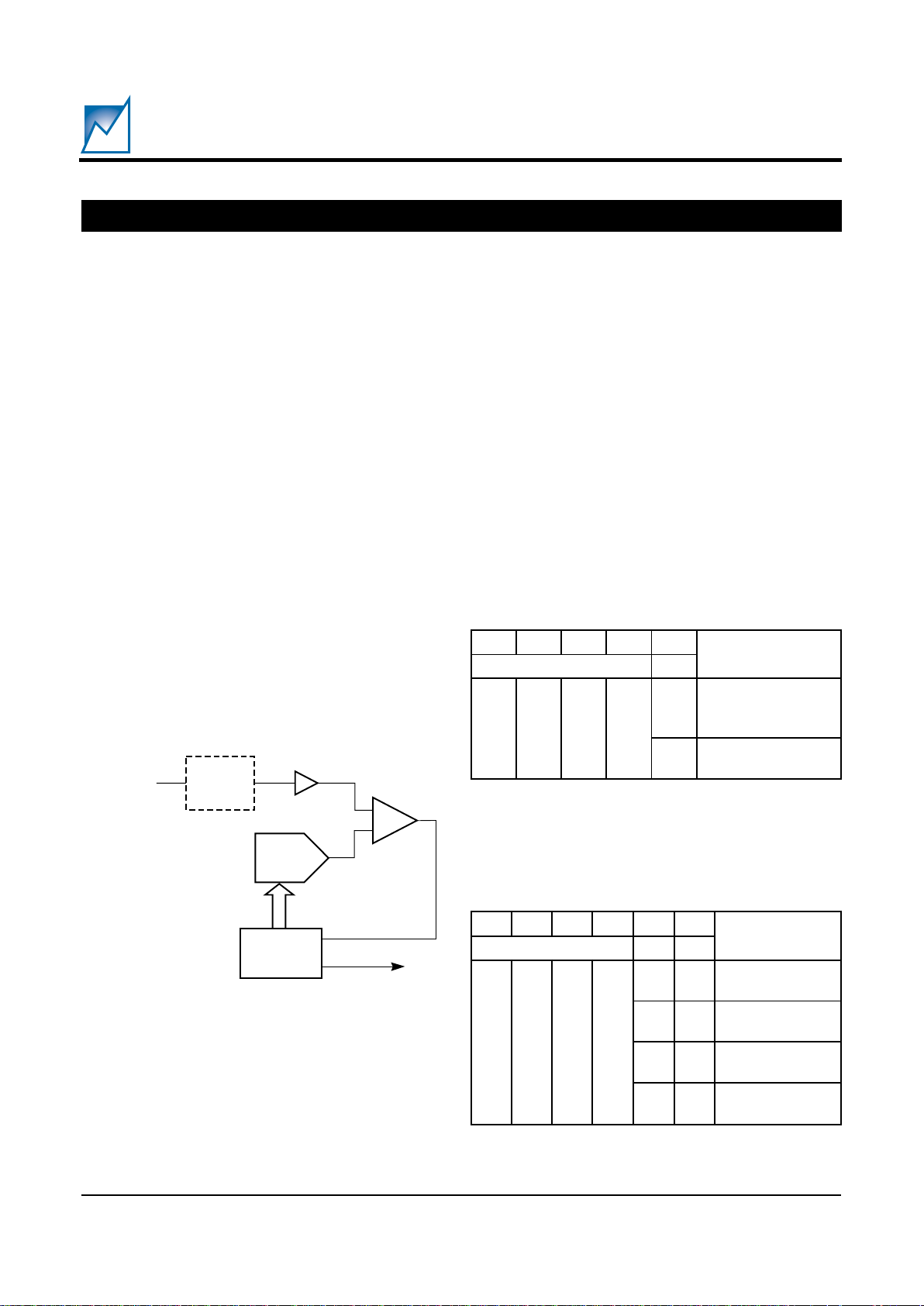
Sample-and-Hold Operation
The channel switching and sampling architecture of the A/
D’s comparator is illustrated in the equivalent input circuit
diagram in Figure 1. During acquisition the selected
channel charges a capacitor in the sample-and-hold circuit. The acquisition interval spans the Acknowledge
period following the command byte and ends on the rising
edge of the next clock. At the end of the acquisition phase
the analog input is disconnected, retaining charge on the
hold capacitor as a sample of the signal.
Figure 1. Sample/Hold and SAR
+
–
2033 Fig01 2.0
Analog In
Buffer
DAC
SAR
Sample
& Hold
SDA
The next bit in the addressing sequence is the EEPROM/
Conversion (E/C) bit; when set to zero the device is
instructed to perform an A/D conversion, and when set to
logic one the EEPROM limit register will be addressed.
See Table 1A.
The next two bits are the channel select bits. Autoincrement is enabled if the channel select bits are set to
11
BIN
and the conversion bit is set to zero. In the autoincrement mode conversions are performed on successive channels, starting with channel 0. After channel 2 is
converted (channel 1 on the SMD1102) the address will
wrap around to channel 0. See Table 1B.
The last bit is the Read/Monitor bit. When the bit is set
to logic one, data can be read from a conversion or from
one of the EEPROM limit registers, depending on the state
of the EEPROM/Conversion bit. When the bit is logic zero
either the auto-monitor mode is entered or the EEPROM
limit register is programmed, again depending on the state
of the EEPROM/Conversion bit. See Table 1C.
Addressing and Command Sequence
All operations of the DAS are preceded first by the start
condition and then by the addressing command sequence. For the SMD1102 & SMD1103 this is 1001
BIN.
For
the SMD1113 it is the binary values of A2, A1, A0, and a
one — a four bit number.
Table 1A. Address Byte — EEPROM/Conversion
7BD6BD5BD4BD3BD
noitcnuF
reifitnedIepyTeciveDC/E
2A
ro
*1
1A
ro
*0
0A
ro
*0
1
0
-nocD/AmrofreP
detcelesnonoisrev
)s(lennahc
1
MORPEEsserddA
retsigertimil
2033 Table01A
* Denotes SMD 1102 & SMD1103. Ax bits are for the SMD1113.
Table 1B. Address Byte — Channel Select
2033 Table01B
* Denotes SMD 1102 & SMD1103. Ax bits are for the SMD1113.
7BD6BD5BD4BD2BD1BD
noitcnuF
reifitnedIepyTeciveD1HC0HC
2A
ro
*1
1A
ro
*0
0A
ro
*0
1
00
0lennahC
detceles
01
1lennahC
detceles
10
2lennahC
detceles
11
fitnemercni-otuA
0=C/E
Page 6

6
SMD1102 / 1103 / 1113
2033 8.1 10/04/01
SUMMIT MICROELECTRONICS, Inc.
Single Channel Conversions
This command sequence is composed of: the Device
Type Identifier, followed by the E/C bit set to zero, then
the channel select bits set to the desired value, and the
R/M bit set to logic one. After the R/M bit is clocked in the
host releases the SDA line and monitors the SDA line for
an acknowledge bit (ACK) from the SMD1102/1103/1113.
The device will drive the SDA line low indicating it received
the command and that it has initiated the acquisition and
conversion on the selected channel. The clock source for
the acquisition and conversion is an internal clock. After
the ACK the SMD1102/1103/1113 will output four dummy
zeros on SDA followed by an echo of the channel’s 2
address bits. The remaining bits in this first byte are the
two MSBs of the conversion. Refer to Figure 2 for a
detailed illustration of this sequence, and for that of
retrieving the remaining conversion byte. The host can
issue a stop condition after retrieving the conversion data
and place the SMD1102/1103/1113 in a low power
standby mode.
Successive Single Channel Conversions
If the host does not issue a stop command after receiving
the last bit of the previous conversion, but instead issues
an ACK and continues clocking, then the SMD1102/1103/
1113 will begin another acquisition and conversion process on the same channel.
Auto-Increment
In the auto-increment mode, the DAS starts a conversion
and then automatically advances to the next channel. The
auto-increment mode always starts at channel 0 and
switches the channel input in the sequence 0, 1, 2, 0, 1,
2, etc. after each successive conversion. The SMD1102,
SMD1103, and SMD1113 independently repeat this pro-
cess so long as the host continues clocking the device,
supplies ACK bits at the appropriate clock interval, and
issues no stop conditions. Refer to Figure 4 for a detailed
illustration of the sequence.
Programming the Limit Registers
Programming the nonvolatile limit registers of the
SMD1102/1103/1113 for use with the auto-monitor function is straightforward. Associated with each channel is
an 11-bit lower limit register and an 11-bit upper limit
register. Ten bits correspond to the 10-bit data, and the
MSB represents the monitor option bit. The monitor option
bits of the upper and lower limit combine to define the alert
region for each channel (described more fully in the
section labeled Alert Conditions). Each limit register
must be programmed separately with a three byte command sequence. To program the limit register the host
first issues a start condition, followed by the device type
identifier, the EEPROM/Conversion (E/C) bit (set to one),
the channel select bits, and the Read/Monitor bit (set to
zero). The second byte consists of four zeroes followed
by the limit select bit (zero = lower limit, one = upper limit),
the monitor option bit, and the two most significant bits of
the limit data. The third byte consists of the remaining
eight bits of limit data. After receiving a stop condition,
the SMD1102/1103/1113 initiates its internal program
sequence. Refer to Figure 5 for details. Six such
sequences are required to set the upper and lower limits
for all three channels. However, once programmed the
data remains stored in EEPROM until reprogrammed.
For example, when a device has both VDD and V
REF
at
5.00V, and an alert must be generated if the voltage on any
channel is ≤2.00V or >3.00V, then the monitor option bits
are set to 10
BIN
, the upper limit is set to 266
HEX
, and the
lower limit is set to 199
HEX
.
Reading the Limit Registers
The timing diagram for reading the limit register data of a
particular channel is shown in Figure 6. The five byte
sequence commences with a start condition, followed by
the device type identifier, the EEPROM/Conversion bit
(set to one), the channel select bits, and the Read/Monitor
bit (set to one). After acknowledging the slave byte the
device outputs a one, followed by an echo of the channel
select bits, a zero, another zero (representing the lower
limit data), the monitor option bit and the two most
significant bits of the limit data. The third byte consists
of the remaining eight bits of the lower limit data. The
fourth byte of the output sequence is the same as the
second byte except the fifth bit is a one (to indicate upper
2033 Table01C
Table 1C. Address Byte — Read/Monitor
* Denotes SMD 1102 & SMD1103. Ax bits are for the SMD1113.
7BD6BD5BD4BD0BD
noitcnuF
reifitnedIepyTeciveDM/R
2A
ro
*1
1A
ro
*0
0A
ro
*0
1
0
rotinom-otuaelbanE
MORPEEetirwro
C/E(retsigertimil
)etats
1
-nocD/AdaeR
MORPEEronoisrev
C/E(retsigertimil
)etats
Page 7

7
2033 8.1 10/04/01
SMD1102 / 1103 / 1113
SUMMIT MICROELECTRONICS, Inc.
Figure 4. Auto-Increment Continuous Read Sequence
Figure 5. Programming the Auto-Monitor Limit Registers
Figure 6. Reading the Auto-Monitor Limit Registers
Monitor
Option
Upper/Lower
1 0 0 U/L0000
A
C
K
S
T
A
R
T
A
C
K
A
C
K
S
T
O
P
D9OP01 E/C CH1 CH0 D8 D7 D6 D5 D4 D3 D2 D1 D0R/M
2033 Fig05
Channel
Address
SCL
SDA
Device Type
Identifier
Figure 2. Single Channel Read Sequence
Channel
Address
Echo
1 0 0 CH1
A
C
K
S
T
A
R
T
A
C
K
A
C
K
D9CH000001 E/C CH1 CH0 D8 D7 D6 D5 D4 D3 D2 D1 D0R/M
2033 Fig03 3.0
Channel
Address
CH1
A
C
K
D9CH00
Conversion #2
00 0 D8 D7 D6
Conversion #1
Channel
Address
SCL
SDA
Device Type
Identifier
Figure 3. Single Channel Continuous Read Sequence
Channel
Address
Echo
1 0 0 CH1
A
C
K
S
T
A
R
T
A
C
K
N
A
C
K
S
T
O
P
D9CH000001 E/C CH1 CH0 D8 D7 D6 D5 D4 D3 D2 D1 D0R/M
2033 Fig02
Channel
Address
SCL
SDA
Device Type
Identifier
Monitor
Option
Lower Limit
100 0
A
C
K
S
T
A
R
T
A
C
K
A
C
K
D9OP01 1 CH1 CH0 D8 D7 D6 D5 D4 D3 D2 D1 D0
R/M
SCL
SDA
2033 Fig06
1 CH1 CH0
0
Monitor
Option
Upper Limit
1
A
C
K
D9OP0 D8 D7 D6 D5 D4 D3 D2 D1 D0
1 CH1 CH0
0
N
A
C
K
S
T
O
P
Channel 0
Address
Echo
1 0 0 CH1
A
C
K
S
T
A
R
T
A
C
K
A
C
K
D9CH000001 CH1 CH0 D8 D7 D6 D5 D4 D3 D2 D1 D0R/M
2033 Fig04
Channel 1
Address
CH1
A
C
K
D9CH00
Conversion #2
Channel 1
00 0 D8 D7 D6
Conversion #1
Channel 0
Channel
Address
= 11
SCL
SDA
Device Type
Identifier
E/C
Page 8

8
SMD1102 / 1103 / 1113
2033 8.1 10/04/01
SUMMIT MICROELECTRONICS, Inc.
stored with the upper and lower limits in the NV registers.
Figure 8 details these conditions. If an out-of-limit
condition is detected the SMD1102/1103/1113 will temporarily remove itself from the auto-increment mode (if that
was selected), and monitor the channel that caused the
alert. There must be five successive conversions resulting in an out-of-limit condition before the SMD1102/1103/
1113 will signal an alert. If at any time during the verify
routine the out-of-limit condition is negated the SMD1102/
1103/1113 will re-enter its Auto-Monitor routine. If a valid
alert condition has been detected the device will halt the
Auto-Monitor function and await instructions from the
host.
If any one of the channels is not being used while the AutoMonitor function is enabled that channel must have its
alert conditions as well as its limit registers set so that it
does not cause an alert. This is accomplished by first
setting the alert region inside the limits (i.e., set monitor
option bits to either 10
BIN
or 11
BIN
), and then setting the
lower limit above the upper limit.
Alert Response
The SMD1102, SMD1103 and SMD1113 are considered
slave devices. They do not generate clocks on the SCL pin
or take control of bus activity. However, the SMBus
specification, an extension of the I2C specification, does
allow slave devices the ability to generate interrupts to get
the attention of the host by pulling SMB
ALERT
# low.
After the SMD1102/1103/1113 has issued an alert by
pulling SMB
ALERT
# low the alert can only be reset by
addressing the device. If there is more than one device
on the SMBus capable of generating an alert, the host may
determine the offending device by issuing an Alert Response Address (ARA). The ARA is a general call to all
devices, but only an SMBus compatible device will recognize the call, and only a device that generated an interrupt
will respond to the call. The DAS responds by acknowledging the ARA, and then by sending its device address
on the SDA line, as shown in Figure 9. Embedded in the
device address is the channel that caused the alert. If
more than one SMBus compliant device has responded
to the ARA, standard I2C bus arbitration allows the device
with the lowest address to be serviced first.
Note: The device address of an SMD1113 should
not be set with A2, A1 and A0 all equal to zero.
This would create an address conflict with the
SMB
ALERT
# broadcast message.
Figure 7. Begin Auto-Monitor Command
100
A
C
K
S
T
A
R
T
10
CH1 CH0
0
2033 Fig07
Channel
Address
SCL
SDA
Device Type
Identifier
S
T
O
P
limit data is forthcoming), and the data bits are from the
upper limit. The fifth and final byte represents the
remaining eight bits of the upper limit data.
Auto-Monitor
Auto-Monitor operation takes full advantage of the unique
capabilities of the SMD1102/1103/1113. Each device can
autonomously monitor the analog channels, compare the
conversion data against stored, nonvolatile limit registers, and, if necessary, alert the host to out-of-limit
conditions. The command string to enter the AutoMonitor mode is shown in Figure 7. It consists of a start
condition followed by the device type identifier (slave
address), the EEPROM/Conversion bit set to zero, the
channel select bits, and the Read/Monitor bit set to zero.
After Acknowledge the host issues a Stop condition in
order to initiate the Auto-Monitor process. Setting the
channel select bits to a particular channel limits the
monitoring to that channel. Setting the channel select bits
to “11” allows all three inputs to be monitored in succession (auto-increment). In the case of the 1102 the limit
registers for channel 2 should be set so that the alert
cannot be generated from this channel (see the following
section "Alert Conditions"). The Auto-Monitor operation
must be terminated before further communication with the
device. The Auto-Monitor function is automatically shut
down when an alert is asserted. Any Read operation will
also halt Auto-Monitor, and, if an alert has occurred, it will
clear the alert along with the stored information of the
channel that prompted the alert.
Note: a Read operation that is used to halt the
Auto-Monitor function will not return valid data.
Alert Conditions
For each channel the host can select one of four conditions that will generate an alert while Auto-Monitor is
active. These conditions are determined by the option bits
Page 9

9
2033 8.1 10/04/01
SMD1102 / 1103 / 1113
SUMMIT MICROELECTRONICS, Inc.
Figure 10. Resetting SMB
ALERT
#
Figure 8. Four Alert Conditions
Figure 9. SMB
ALERT
# Response Sequence
0011
A
C
K
N
A
C
K
S
T
A
R
T
S
T
O
P
0 CH1 CH0
2033 Fig10
SCL
SMB
ALERT#
SDA
R/M
Once the SMB
ALERT
# signal has been asserted it must be
reset before further communication with the device, with
the exception of the SMB
ALERT
# response sequence.
Resetting the SMB
ALERT
# is accomplished by performing
a read operation.
Figure 10 shows the SMB
ALERT
# signal being reset by a
Read operation.
Note: a Read operation that is used to reset the
SMB
ALERT
# will not return valid data.
Monitor
Option Bits
x x
Lower
Upper
2033 Fig08
ALERT
REGION
ALERT
REGION
ALERT
REGION
ALERT
REGION
3FF
Solid line
indicates
alert set if
conv = limit
Upper limit
Dashed line
indicates
alert NOT set
if conv = limit
000
"00" "01"
"10" "11"
3FF
000
ALERT
REGION
ALERT
REGION
3FF
000
3FF
000
Lower limit
Device Type
Identifier
0010 CH1
A
C
K
N
A
C
K
S
T
A
R
T
S
T
O
P
CH010 0 1 1000R/M
2033 Fig09
Alert Response
Address
SCL
SMB
ALERT
#
SDA
Offending Channel
Address
Page 10

10
SMD1102 / 1103 / 1113
2033 8.1 10/04/01
SUMMIT MICROELECTRONICS, Inc.
Table 2. Register Read/Write AC Operating Characteristics
GENERAL DESCRIPTION
The I
2
C bus is a two-way, two-line serial communication
between different integrated circuits. The two lines are: a
serial Data line (SDA) and a serial Clock line (SCL). All
Summit Microelectronics parts support a 100kHz clock
rate, and some support the alternative 400kHz clock.
Check Table 2 for the value of f
SCL
. The SDA line must be
connected to a positive supply by a pull-up resistor located
on the bus. Summit parts have a Schmitt input on both
lines. See Figure 11 and Table 2 for waveforms and timing
on the bus. One bit of Data is transferred during each
Clock pulse. The Data must remain stable when the Clock
is high.
BUS INTERFACE
2033 Table02
Figure 11. Interface Bus Timing
lobmySretemaraPsnoitidnoC.niM.xaMstinU
f
LCS
ycneuqerfkcolcLCS 0001zHk
t
WOL
doirepwolkcolC 7.4sµ
t
HGIH
doirephgihkcolC 0.4sµ
t
FUB
)1(emiteerfsuBnoissimsnartwenerofeB7.4sµ
t
ATS:US
emitputesnoitidnoctratS 7.4sµ
t
ATS:DH
emitdlohnoitidnoctratS 0.4sµ
t
OTS:US
emitputesnoitidnocpotS 7.4sµ
t
AA
tuptuodilavotegdekcolC)nelcyc(ADSdilavotwolLCS3.05.3sµ
t
HD
)1(emitdlohtuOataDegnahcADSot)1+nelcyc(wolLCS3.0sµ
t
R
)1(emitesirADSdnaLCS 0001sn
t
F
)1(emitllafADSdnaLCS 003sn
t
TAD:US
)1(emitputesnIataD 052sn
t
TAD:DH
)1(emitdlohnIataD 0sn
IT)1(ADSdnaLCSretlifesioNnoisserppusesioN001sn
t
RW
emitelcycetirW 5sm
Note (1) These values are guaranteed by design.
t
F
t
R
t
LOW
t
HIGH
t
HD:STA
t
SU:STA
t
BUF
t
DH
t
HD:DAT
t
SU:DAT
t
SU:STO
SCL
SDA In
SDA Out
t
AA
2033 Fig11
Page 11

11
2033 8.1 10/04/01
SMD1102 / 1103 / 1113
SUMMIT MICROELECTRONICS, Inc.
Start and Stop Conditions
Both Data and Clock lines remain high when the bus is not
busy. Data transfer between devices may be initiated with
a Start condition only when SCL and SDA are high. A highto-low transition of the Data line while the Clock line is high
is defined as a Start condition. A low-to-high transition of
the Data line while the Clock line is high is defined as a Stop
condition. See Figure 12.
Acknowledge
Data is always transferred in 8-Bit bytes. Acknowledge
(ACK) is used to indicate a successful data transfer. The
Transmitting device will release the bus after transmitting
eight bits. During the ninth clock cycle the Receiver will
pull the SDA line low to Acknowledge that it received the
eight bits of data (See Figure 13). The termination of a
Master Read sequence is indicated by a non-Acknowledge (NACK), where the Master will leave the Data line
high.
In the case of a Read from a Summit part, when the last
byte has been transferred to the Master, the Master will
leave the Data line high for a NACK. This will cause the
Summit part to stop sending data, and the Master will issue
a Stop on the clock pulse following the NACK.
In the case of a Write to a Summit part the Master will send
a Stop on the clock pulse after the last Acknowledge. This
will indicate to the Summit part that it should begin its
internal nonvolatile write cycle.
Read and Write
The first byte from a Master is always made up of the eight
bits illustrated in Table 1.
In the read mode the SMD1102/1103/1113 transmits eight
bits of data, then releases the SDA line, and monitors the
line for an Acknowledge signal. If an Acknowledge is
detected, and no STOP condition is generated by the
Master, the device will continue to transmit data. If an
Acknowledge is not detected (NACK), the device will
terminate further data transmission.
In the write mode the SMD1102/1103/1113 receives eight
bits of data, then generates an Acknowledge signal. It will
continue to generate ACKs until a STOP condition is
generated by the Master.
Protocol
The protocol defines any device that sends data onto the
bus as a Transmitter, and any device that receives data as
a Receiver. The device controlling data transmission is
called the Master, and the controlled device is called the
Slave. In all cases the Summit Microelectronic devices
are slave devices, since they never initiate any data
transfers.
2033 Fig10
SCL
SDA In
START
Condition
STOP
Condition
Figure 12. Start and Stop Conditions
Figure 13. Acknowledge Timing
SCL
SDA
Trans
SDA
Rec
1
2
3
8
9
ACK
2033 Fig11
Page 12

12
SMD1102 / 1103 / 1113
2033 8.1 10/04/01
SUMMIT MICROELECTRONICS, Inc.
PACKAGES
8 PIN PDIP PACKAGE
8 PIN SOIC PACKAGE
PIN 1 INDICATOR
.015
(.381)
.100
(2.54)
0.014 - 0.022
(0.36 - 0.56)
SEATING PLANE
0.008 - 0.014
(0.20 - 0.36)
8 Pin PDIP
0.300 - 0.325
(7.62 - 8.25)
0.43
(10.9)
MAX.
0.21
(5.33)
MAX.
0.115 - 0.195
(2.92 - 4.95)
0.115 - 0.195
(2.92 - 4.95)
Min.
1
0.24 - 0.28
(6.1 - 7.1)
0.355 - 0.400
(9.02 - 10.2)
0.045 - 0.070
(1.14 - 1.78)
Ref. JEDEC MS-001
Inches
(Millimeters)
.05 (1.27) TYP.
1
8 Pin SOIC
0.150 - 0.157
(3.80 - 4.00)
0.189 - 0.196
(4.80 - 5.00)
0.053 - 0.069
(1.35 - 1.75)
0.013 - 0.020
(0.33 - 0.51)
0.004 - 0.010
(0.10 - 0.25)
0.016 - 0.050
(0.40 - 1.27)
×45º
0.010 - 0.020
(0.25 - 0.50)
0.228 - 0.244
(5.80 - 6.20)
Ref. JEDEC MS-012
Inches
(Millimeters)
Page 13

13
2033 8.1 10/04/01
SMD1102 / 1103 / 1113
SUMMIT MICROELECTRONICS, Inc.
14 PIN SOIC PACKAGE
0.150 - 0.157
0.013 - 0.020
(0.33 - 0.51)
0.004 - 0.01
(0.10 - 0.25)
0.337 - 0.344
(8.55 - 8.75)
0.228 - 0.244
(5.80 - 6.20)
0.053 - 0.069
(1.35 - 1.75)
0.016 - 0.050
(0.40 - 1.27)
(1.27)
0.0075 - 0.01
(0.19 - 0.25)
0.01 - 0.02
(0.25 - 0.50)
(3.80 - 4.00)
14 Pin SOIC
×45º
0.016 - 0.050
0.05
0 to 8
typ
1
Ref. JEDEC MS-012
Inches
(Millimeters)
ORDERING INFORMATION
SMD110
2
S
Base Part Number
Package
Type
2 = REF
IN
3 = AIN2
S = SOIC
P = PDIP
2033 Tree 8
SMD1113
S
Base Part Number
Package
S = SOIC
2033 Tree 14
Page 14

14
SMD1102 / 1103 / 1113
2033 8.1 10/04/01
SUMMIT MICROELECTRONICS, Inc.
NOTICE
SUMMIT Microelectronics, Inc. reserves the right to make changes to the products contained in this publication in
order to improve design, performance or reliability. SUMMIT Microelectronics, Inc. assumes no responsibility for
the use of any circuits described herein, conveys no license under any patent or other right, and makes no
representation that the circuits are free of patent infringement. Charts and schedules contained herein reflect
representative operating parameters, and may vary depending upon a user’s specific application. While the
information in this publication has been carefully checked, SUMMIT Microelectronics, Inc. shall not be liable for any
damages arising as a result of any error or omission.
SUMMIT Microelectronics, Inc. does not recommend the use of any of its products in life support or aviation applications
where the failure or malfunction of the product can reasonably be expected to cause any failure of either system or to
significantly affect their safety or effectiveness. Products are not authorized for use in such applications unless
SUMMIT Microelectronics, Inc. receives written assurances, to its satisfaction, that: (a) the risk of injury or damage has
been minimized; (b) the user assumes all such risks; and (c) potential liability of SUMMIT Microelectronics, Inc. is
adequately protected under the circumstances.
Power Management for Communications™
This document supersedes all previous versions.
© Copyright 2001 SUMMIT Microelectronics, Inc.
I2C is a trademark of Philips Corporation.
PART MARKING
.
SUMMIT
SMD1113S
L YY WW
Package type - SOIC (S)
L
= Lot number
YY
= Year
WW
= Work Week
SMD1113
Ê
.
SUMMIT
SMD1103
n
L YY WW
n
= Package type (P or S)
L
= Lot number
YY
= Year
WW
= Work Week
.
SUMMIT
SMD1103
n
L YY WW
02
SMD1102
SMD1103
Ê
Ê
 Loading...