

Datasheet SMCJ5.0A-TR, SMCJ5.0CA-TR, SMCJ6.5CA-TR, SMCJ6.0A-TR, SMCJ6.5A-TR Datasheet (SGS Thomson Microelectronics)
...Page 1
SMCJ5.0A-TR,CA-TR
®
FEATURES
PEAK PULSE POW ER : 1500 W (10/1000µs)
STAND OFF VOLTAGE RANGE :
From 5V to 188V.
UNI AND BID IRECTIONA L T YPES
LOW CLAMPING FACTO R
FAST RESPONSE TIME
DESCRIPTION
TM
The SMCJ series are TRANSIL
diodes designed
specifically for protecting sensitive equipment
against transient overvoltages.
Transil diodes provide high overvoltage protection
by clamping action. Their instantaneous response
to trans ient over voltage s makes them pa rticula rly
suite d to prot ect volt age sensit ive devic es such
as MOS Technology and low voltage supplied
IC’s.
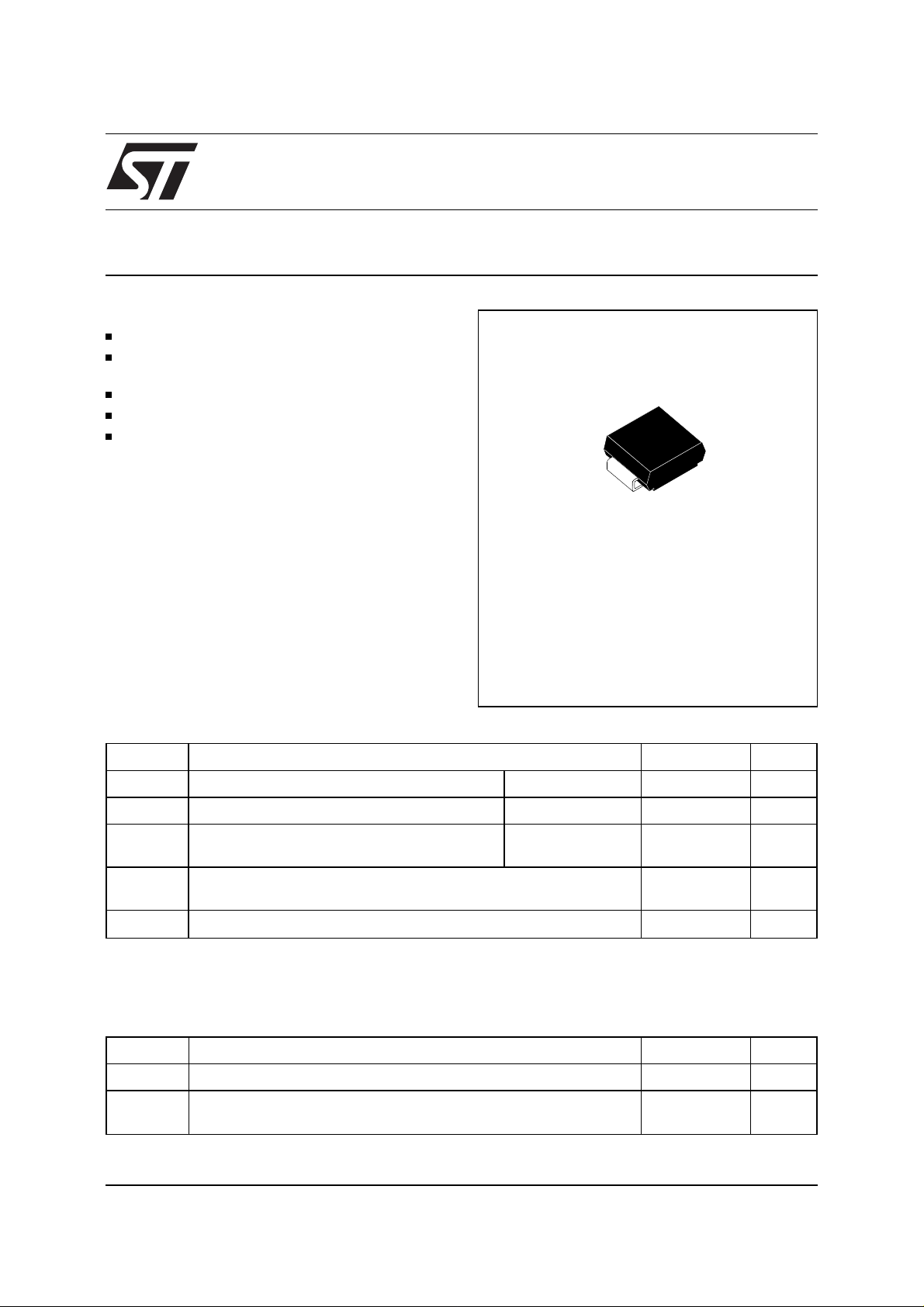
SMCJ188A-TR,CA-TR
TRANSIL
SMC
(JEDEC DO-214AB)
TM
ABSOL UTE M AXIMU M RA TIN GS (T
amb
= 25°C)
Symbol Parameter Value Unit
P
PP
P Power dissipation on infinite heatsink T
I
FSM
T
stg
T
j
T
L
Note 1
: For a surge greater than the maximum valu es, the diode wil l fail in short-ci rcuit.
Peak pulse power dissipation (see note 1) Tj initial = T
°C6.5W
Non repetitive surge peak forward
current for unidirectional types
amb = 50
tp = 10ms
Tj initial = T
Storage temperature range
Maximum junction temperature
amb
amb
1500 W
200 A
- 65 to + 175
150
Maximum lead temperature for soldering during 10 s. 260 °C
THERMAL RE SISTA NC ES
Symbol Parameter Value Unit
R
R
th (j-l)
th (j-a)
Junction to leads 15 °C/W
Junction to ambient on printed circuit on recommended pad
75 °C/W
layout
August 1999 - Ed: 5A
°C
°C
1/5
Page 2
SMCJxxxA-TR, CA-TR
ELECTRICAL CHARACTERISTICS (T
Symbol Parameter
V
RM
V
BR
V
CL
I
RM
I
PP
α
T Voltage temperature coefficient
V
F
Unidirectional Mark. Bidirectional Mark.µAV VmAV A V A10
SMCJ5.0A-TR FUA SMCJ5.0CA-TR FBA 800 5.0 6.4 10 9.2 171 13.4 746 5.7 9500
SMCJ6.0A-TR FUB SMCJ6.0CA-TR FBB 800 6.0 6.7 10 10.3 152 13.7 730 5.9 9000
SMCJ6.5A-TR FUC SMCJ6.5CA-TR FBC 500 6.5 7.2 10 11.2 140 14.5 690 6.1 8500
SMCJ8.5A-TR FUD SMCJ8.5CA-TR FBD 5 8.5 9.4 1 14.4 105 19.5 512 7.3 7000
SMC10A-TR FUF SMCJ10CA-TR FBF 5 10 11.1 1 17 92 21.7 461 7.8 6000
SMCJ12A-TR FUH SMCJ12CA-TR FBH 5 12 13.3 1 19.9 79 25.3 394 8.3 5250
SMCJ13A-TR FUI SMCJ13CA-TR FBI 1 13 14.4 1 21.5 73 27.2 368 8.4 5000
SMCJ15A-TR FUJ SMCJ15CA-TR FBJ 1 15 16.7 1 24.4 64 32.5 308 8.8 4300
SMCJ18A-TR FUL SMCJ18CA-TR FBL 1 18 20 1 29.2 53 39.3 254 9.2 3700
SMCJ20A-TR FUM SMCJ20CA-TR FBM 1 20 22.2 1 32.4 48 42.8 234 9.4 3500
SMCJ22A-TR FUN SMCJ22CA-TR FBN 1 22 24.4 1 35.5 44 48.3 207 9.6 3200
SMCJ24A-TR FUO SMCJ24CA-TR FBO 1 24 26.7 1 38.9 40 50 200 9.6 3050
SMCJ26A-TR FUP SMCJ26CA-TR FBP 1 26 28.9 1 42.1 37 53.5 187 9.7 2900
SMCJ28A-TR FUQ SMCJ28CA-TR FBQ 1 28 31.1 1 45.4 34 59 169 9.8 2700
SMCJ30A-TR FUR SMCJ30CA-TR FBR 1 30 33.3 1 48.4 32 64.3 156 9.9 2500
SMCJ33A-TR FUS SMCJ33CA-TR FBS 1 33 36.7 1 53.3 29 69.7 143 10.0 2400
SMCJ40A-TR FUU SMCJ40CA-TR FBU 1 40 44.4 1 64.5 24 84 119 10.1 2050
SMCJ48A-TR FUW SMCJ48CA-TR FBW 1 48 53.3 1 77.4 20 100 100 10.3 1800
SMCJ58A-TR FUZ SMCJ58CA-TR FBZ 1 58 64.4 1 93.6 16 121 83 10.4 1550
SMCJ60A-TR GUA SMCJ60CA-TR GBA 1 60 66.5 1 96.6 15.7 125 81 10.5 1520
SMCJ70A-TR GUB SMCJ70CA-TR GBB 1 70 77.8 1 113 13.9 146 69 10.5 1350
SMCJ85A-TR GUE SMCJ85CA-TR GBE 1 85 94.4 1 137 11.5 178 56 10.6 1150
SMCJ100A-TR GUG SMCJ100CA-TR GBG 1 100 111 1 162 9.7 212 47 10.7 1000
SMCJ130A-TR GUI SMCJ130CA-TR GBI 1 130 144 1 209 7.5 265 38 10.8 850
SMCJ154A-TR GUL SMCJ154CA-TR GBL 1 154 171 1 246 6.1 317 31.5 10.8 725
SMCJ170A-TR GUM SMCJ170CA-TR GBM 1 170 189 1 275 5.7 353 28 10.8 675
SMCJ188A-TR GUN SMCJ188CA-TR GBN 1 188 209 1 328 4.6 388 26 10.8 625
Stand-off voltage
Breakdown voltage
Clamping voltage
Leakage current @ V
Peak pulse current
Forward voltage drop
Types
RM
amb
= 25°C)
I
RM
VVCLV
BR
V
RM
@ VRMVBR @ IRVCL @ I
I
I
F
I
RM
I
PP
PPVCL
V
@ I
F
PP
max min max max max typ
note2 10/1000µs 8/20µs note3 note4
V
TC
α
-4
/°CpF
2/5
100
%I
PP
10 s
50
0
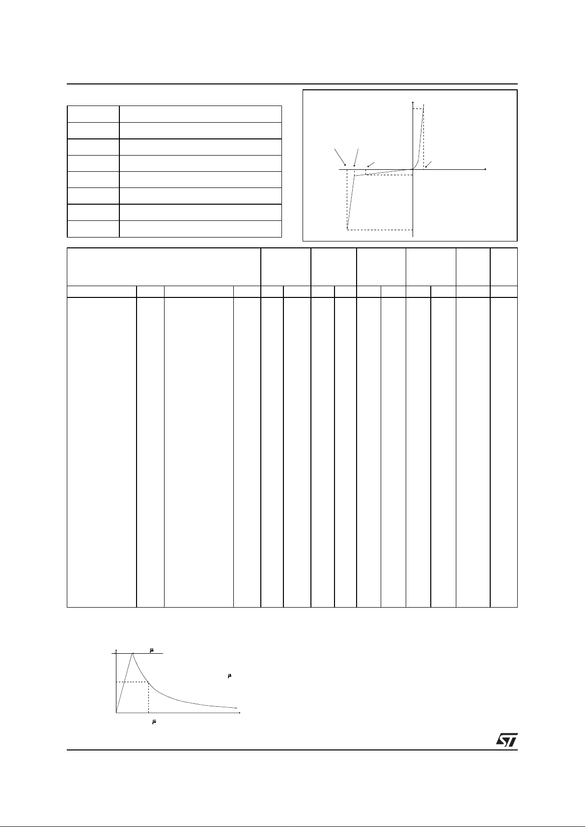
PULSE WAVEFORM 10/1000 s
1000 s
t
Note 2 :
Pulse test : tp < 50 ms.
Note 3 :
Note 4 :
capacitance value is divided by 2.
VBR = αT * (T
∆
VR = 0 V, F = 1 MHz. For bidirectional types,
- 25) * VBR(25°C).
amb
Page 3

ORDER CODE
SMCJxxxA- TR, CA- T R
SM C J 85 C A - TR
SURFACE MOUNT
1500 WATTS
STAND OFF VOLTAGE
Fig. 1: Peak power dissipation versus initial junction temperature.
Ppp[Tj initial]/Pp p [T j initial=25°C]
1.1
1.0
0.9
0.8
0.7
0.6
0.5
0.4
0.3
0.2
0.1
0.0
0 25 50 75 100 125 150 175
Tj initial(°C)
TAPE & REEL
BIDIRECTIONAL
No suffix : Unidirectional
Fig. 2: Continous power dissipation versus initial
junction temperature.
P(W)
8
Rth(j-a)=Rth(j-l)
7
6
5
4
3
Rth(j-a)=75°C/W
2
1
0
0 25 50 75 100 125 150
Tamb(°C)
Fig. 3: Peak pulse power versus exponential pulse
duration (Tj initial=25°C).
Ppp(kW)
50.0
10.0
1.0
0.1
0.01 0.10 1.00 10.00
tp(ms)
Fig. 4: Clamping voltage versus peak pulse current (Tj initial=25°C).
Exponential waveform tp=20µs & tp=1ms.
Ipp(A)
1E+3
1E+2
1E+1
1E+0
1E-1
1 10 100 1000
SMCJ5.0A,CA
tp=20µs
SMCJ8.5A,CA
Vcl(V)
SMCJ18A,CA
SMCJ33A,CA
SMCJ58A,CA
SMCJ130A,CA
SMCJ188A,CA
tp=1ms
3/5
Page 4

SMCJxxxA-TR, CA-TR
Fig. 5-1: Capacitance versus reverse applied volt-
age (typical values) ( SMCJx xA serie).
C(nF)
10.00
1.00
SMCJ5.0A
SMCJ18A
SMCJ33A
F=1MHz
SMCJ58A
SMCJ188A
0.10
0.01
1 10 100 200
VR(V)
Fig. 6: Peak forward voltage drop versus peak forward current (typical values).
IFM(A)
200.0
100.0
Tj=125°C
Fig. 5-2: Capacitance versus reverse applied voltage (typical values) (SMCJxxCA serie).
C(nF)
10.00
SMCJ5.0CA
1.00
SMCJ18CA
SMCJ33CA
0.10
0.01
1 10 100 200
F=1MHz
SMCJ58CA
SMCJ188CA
VR(V)
Fig. 7: Relative variation of thermal impedance
junction to ambient versus puls e dur ation.
(Printed circuit board FR4, S (C u)=1cm
Zth(j-a)/Rth(j-a)
1.00
2
).
10.0
Tj=25°C
1.0
0.1
0.5 1.0 1.5 2.0 2.5 3.0 3.5
VFM(V)
Fig. 8: Thermal resistance junction to ambient versus copper surface under each lead
(Printed circuit board FR4, e(Cu)=35µm)
Rth(j-a) (°C/W)
100
90
80
70
60
50
40
012345
S(cm²)
0.10
0.01
1E-2 1E-1 1E+0 1E+1 1E+2 5E+2
tp(s)
Fig. 9: Relative variation of leakage current versus
junction temperature.
IR[Tj] / IR [Tj=25° C ]
2E+3
1E+3
1E+2
1E+1
1E+0
1E-1
0 25 50 75 100 125 150
Tj(°C)
VBR upper or
equal to 8.5V
VBR<8.5V
4/5
Page 5

SMCJxxxA- TR, CA- T R
MARKING : Logo, Date Code, Type Code, Cathode Band (for unidirectional types only).
PACKAGE ME CHANICAL D AT A
SMC (Plastic)
DIMENSIONS
E1
D
E
A1
C
L
E2
A2
FOOTPRINT DIMENSIONS (Millimeter)
SMC Plastic.
b
REF.
Millimeters Inches
Min. Max. Min. Max.
A1 1.90 2.45 0.075 0.096
A2 0.05 0.20 0.002 0.008
b 2.90 3.2 0.114 0.126
c 0.15 0.41 0.006 0.016
E 7.75 8.15 0.305 0.321
E1 6.60 7.15 0.260 0.281
E2 4.40 4.70 0.173 0.185
D 5.55 6.25 0.218 0.246
L 0.75 1.60 0.030 0.063
3.3
2.0 4.2 2.0
Packaging
Weight
Information furnished is believed to be accurate and reliable. However, STMicroelectronics assumes no responsibility for the consequences of
use of such information nor for any infringement of patents or other rights of third parties which may result from its use. No license is granted by
implication or otherwi se un der any pat ent or patent rights of STMic roelec tronics. S pecifications ment ioned in t his publ ication are subject to
change without notice. This publication supersedes and replaces all information previously supplied.
STMicroelectronics products ar e not authorized for use as crit ic al components in life support devices or systems wi thout express wri tte n approval of STMicroelectronics.
: standard packaging is in tape and reel.
: 0.25 g
The ST logo is a registered trademark of STMicroe lectronics
© 1999 STMicroelectronics - Printed in Italy - All rights reser ved.
STMicroelectronics GROUP OF COMPANIES
Australia - Brazil - China - Finland - France - Germany - Hong Kong - India - Italy - Japan - Malaysia
Malta - Morocco - Singapore - Spain - Sweden - Switzerland - United Kingdom - U.S.A.
http://www.st.com
5/5
 Loading...