

Datasheet SMBJ16A-TR, SMBJ5.0A-TR, SMBJ5.0CA-TR, SMBJ6.5CA-TR, SMBJ6.0A-TR Datasheet (SGS Thomson Microelectronics)
...Page 1

SMBJ5.0A-TR,CA-TR
®
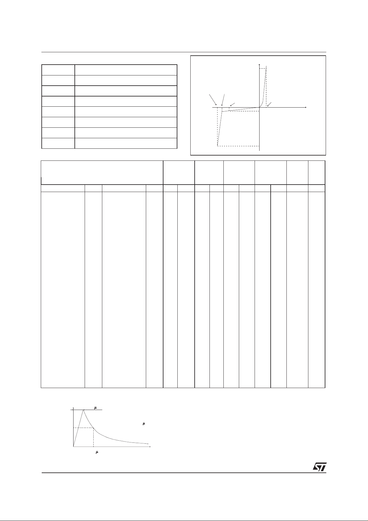
FEATURES
PEAK PULSE POWER : 600 W (10/1000µs)
■
STAND OFF VOLTAGE RANGE :
■
From 5V to 188V.
UNI AND BIDIRECTIONAL TYPES
■
LOW CLAMPING FACTOR
■
FAST RESPONSE TIME
■
JEDEC REGISTERED PACKAGE OUTLINE
■
DESCRIPTION
The SMBJ series are TRANSIL
TM
diodes designed
specifically for protecting sensitive equipment
against transient overvoltages.
Transil diodes provide high overvoltage protection
by clamping action. Their instantaneous response
to transient overvoltages makes them particularly suited to protect voltage sensitive devices
such as MOS Technology and low voltage supplied IC’s.
SMBJ188A-TR,CA-TR
TRANSIL
SMB
(JEDEC DO-214AA)
TM
ABSOLUTE MAXIMUM RATINGS (T
amb
= 25°C)
Symbol Parameter Value Unit
P
PP
P
I
FSM
T
stg
T
j
T
L
Note 1 : For a surge greater than the maximum values, the diode will fail in short-circuit.
Peak pulse power dissipation (see note 1) Tj initial = T
Power dissipation on infinite heatsink T
Non repetitive surge peak forward
current for unidirectional types
= 50°C
amb
tp = 10ms
Tj initial = T
Storage temperature range
Maximum junction temperature
Maximum lead temperature for soldering during 10 s.
amb
amb
600 W
5W
100 A
-65to+175
150
260 °C
THERMAL RESISTANCES
Symbol Parameter Value Unit
R
R
th (j-l)
th (j-a)
Junction to leads
Junction to ambient on printed circuit on recommended pad
20 °C/W
100 °C/W
layout
°C
°C
October 2001- Ed: 4
1/6
Page 2
SMBJxxxA-TR, CA-TR
ELECTRICAL CHARACTERISTICS (T
Symbol Parameter
V
RM
V
BR
V
CL
I
RM
I
PP
Stand-off voltage
Breakdown voltage
Clamping voltage
Leakage current @ V
Peak pulse current
RM
amb
= 25°C)
VVCLV
BR
I
I
F
V
RM
V
F
I
RM
V
αT Voltage temperature coefficient
V
F
Unidirectional Mark. Bidirectional Mark. µAVVmAVAVA10
SMBJ5.0A-TR BUZ SMBJ5.0CA-TR BBZ 800 5.0 6.4 10 9.2 68 13.4 298 5.7 4000
SMBJ6.0A-TR BUA SMBJ6.0CA-TR BBA 800 6.0 6.7 10 10.3 61 13.7 290 5.9 3850
SMBJ6.5A-TR BUB SMBJ6.5CA-TR BBB 500 6.5 7.2 10 11.2 56 14.5 276 6.1 3700
SMBJ8.5A-TR BUC SMBJ8.5CA-TR BBC 5 8.5 9.4 1 14.4 41.7 19.5 205 7.3 2800
SMBJ10A-TR BUD SMBJ10CA-TR BBD 5 10 11.1 1 17 37 21.7 184 7.8 2300
SMBJ12A-TR BUE SMBJ12CA-TR BBE 5 12 13.3 1 19.9 31 25.3 157 8.3 2025
SMBJ13A-TR BUF SMBJ13AC-TR BBF 1 13 14.4 1 21.5 29 27.2 147 8.4 1900
SMBJ15A-TR BUG SMBJ15CA-TR BBG 1 15 16.7 1 24.4 25.1 32.5 123 8.8 1600
SMBJ16A-TR CUG SMBJ16CA-TR CBG 1 16 17.8 1 26 23.1 32.5 123 8.8 1600
SMBJ18A-TR BUH SMBJ18CA-TR BBH 1 18 20 1 29.2 21.5 39.3 102 9.2 1350
SMBJ20A-TR BUI SMBJ20CA-TR BBI 1 20 22.2 1 32.4 19.4 42.8 93 9.4 1250
SMBJ22A-TR BVA SMBJ22CA-TR CBH 1 22 24.4 1 35.5 17.7 48.3 83 9.6 1150
SMBJ24A-TR BUJ SMBJ24CA-TR BBJ 1 24 26.7 1 38.9 16 50 80 9.6 1112
SMBJ26A-TR BUK SMBJ26CA-TR BBK 1 26 28.9 1 42.1 14.9 53.5 75 9.7 1075
SMBJ28A-TR BUL SMBJ28CA-TR BBL 1 28 31.1 1 45.4 13.8 59 68 9.8 1000
SMBJ30A-TR BUM SMBJ30CA-TR BBM 1 30 33.3 1 48.4 13 64.3 62 9.9 950
SMBJ33A-TR BUN SMBJ33CA-TR BBN 1 33 36.7 1 53.3 11.8 69.7 57 10.0 900
SMBJ40A-TR CUJ SMBJ40CA-TR CBJ 1 40 44.4 1 64.5 9.7 84 48 10.1 800
SMBJ48A-TR BUW SMBJ48CA-TR BBW 1 48 53.3 1 77.4 8.1 100 40 10.3 700
SMBJ58A-TR BUO SMBJ58CA-TR BBO 1 58 64.4 1 93.6 6.7 121 33 10.4 625
SMBJ70A-TR CUM SMBJ70CA-TR CBM 1 70 77.8 1 113 5.5 146 27 10.5 550
SMBJ85A-TR BUQ SMBJ85CA-TR BBQ 1 85 94.4 1 137 4.6 178 22.5 10.6 500
SMBJ100A-TR CUQ SMBJ100CA-TR CBQ 1 100 111 1 162 3.8 212 19 10.7 450
SMBJ130A-TR BUS SMBJ130CA-TR BBS 1 130 144 1 209 3 265 15 10.8 400
SMBJ154A-TR BUT SMBJ154CA-TR BBT 1 154 171 1 246 2.4 317 12.6 10.8 360
SMBJ170A-TR BUU SMBJ170CA-TR BBU 1 170 189 1 275 2.2 353 11.3 10.8 350
SMBJ188A-TR BUV SMBJ188CA-TR BBV 1 188 209 1 328 2 388 10.3 10.8 330
Forward voltage drop
Types
I
PP
I
RM@VRMVBR@IRVCL@IPPVCL@IPP
αTC
max. min. max. max. max. typ.
note2 10/1000µs 8/20µs note3 note4
-4
/°C pF
2/6
100
%I
PP
10 s
50
0
PULSE WAVEFORM 10/1000 s
1000 s
t
Note 2 : Pulse test : tp<50ms.
Note 3 : ∆VBR= αT*(T
Note 4 : VR= 0 V, F = 1 MHz. For bidirectional types,
capacitance value is divided by 2.
- 25)*VBR(25°C).
amb
Page 3

Fig. 1: Peak pulse power dissipation versus initial
junction temperature (printed circuit board).
Fig. 2 : Peak pulse power versus exponential pulse duration.
SMBJxxxA-TR, CA-TR
3/6
Page 4

SMBJxxxA-TR, CA-TR
Fig. 3 : Clamping voltage versus peak pulse current.
Exponential waveform t
SMBJ188A
SMBJ130A
SMBJ58A
SMBJ33A
SMBJ18A
SMBJ8.5A
SMBJ5.0A
=20µs ________
p
= 1 ms ——————-
t
p
= 10 ms ...............
t
p
Note : The curves of the figure 3 are specified for a junction temperature of 25 ⊃C before surge.
The given results may be extrapolated for other junction temperatures by using the following formula :
∆V
= αT*[T
BR
-25]*VBR(25°C)
amb
For intermediate voltages, extrapolate the given results.
Fig. 4a : Capacitance versus reverse applied
voltage for unidirectional types (typical values).
C (pF)
10000
Tj = 25°C
S
M
B
J
5
.
0
S
1000
S
S
S
100
10
110100
A
M
B
J
1
3
A
M
B
J
2
6
A
M
B
J
5
8
A
M
B
J
1
8
8
A
F= 1 MHz
V(V)
R
500
Fig. 4b : Capacitance versus reverse applied
voltage for bidirectional types (typical values).
C (pF)
10000
S
MBJ
5.
0
A
S
MBJ
1000
100
10
13A
S
MBJ
26
MBJ
MBJ
1
58
88
A
A
A
S
S
110100
Tj = 25°C
F= 1 MHz
V(V)
R
500
4/6
Page 5

SMBJxxxA-TR, CA-TR
Fig. 5 : Peak forward voltage drop versus peak
forward current (typical values for unidirectional
types).
Fig. 7 : Relative variation of leakage current
versus junction temperature.
Fig. 6 : Transient thermal impedance junction-ambient versus pulse duration.
Mounting on FR4 PC Board with Recommended
pad layout.
ORDER CODE
SURFACE MOUNT
600W
SM B J 85 C A -TR
TAPE & REEL
BIDIRECTIONAL
No suffix: Unidirectional
STAND OFFVOLTAGE
5/6
Page 6

SMBJxxxA-TR, CA-TR
MARKING : Logo, Date Code, Type Code, Cathode Band (for unidirectional types only).
PACKAGE MECHANICAL DATA
SMB (Plastic)
DIMENSIONS
E1
REF.
Millimeters Inches
Min. Typ. Max. Min. Typ. Max.
D
E
A1
c
L
A2
FOOTPRINT DIMENSIONS (Millimeter)
SMD Plastic.
2.3
1.52 2.75
1.52
A1 1.90 2.15 2.45 0.075 0.085 0.096
A2 0.05 0.15 0.20 0.002 0.006 0.008
b 1.95 2.20 0.077 0.087
c 0.15 0.41 0.006 0.016
E 5.10 5.40 5.60 0.201 0.213 0.220
E1 4.05 4.30 4.60 0.159 0.169 0.181
b
D 3.30 3.60 3.95 0.130 0.142 0.156
L 0.75 1.15 1.60 0.030 0.045 0.063
Packaging : standard packaging is in tape and reel.
SOD15 = Standard packaging is in Film.
Weight : 0.12 g
Informationfurnishedisbelievedto be accurateand reliable. However,STMicroelectronics assumes noresponsibility for theconsequences of
useof such information nor for any infringementof patents or other rights of third parties which mayresult from its use. No license isgranted by
implication or otherwise under any patent or patent rights of STMicroelectronics. Specifications mentioned in this publication are subject to
change without notice. This publication supersedes and replaces all information previously supplied.
STMicroelectronics products are not authorized for use as critical components in life support devices or systems without express written
approval of STMicroelectronics.
The ST logo is a registered trademark of STMicroelectronics
© 2001 STMicroelectronics - Printed in Italy - All rights reserved.
STMicroelectronics GROUP OF COMPANIES
Australia - Brazil - China - Finland - France - Germany - Hong Kong - India - Italy - Japan - Malaysia
Malta - Morocco - Singapore - Spain - Sweden - Switzerland - United Kingdom - U.S.A.
http://www.st.com
6/6
 Loading...