

Datasheet SMAJ5.0A-TR, SMAJ5.0CA-TR, SMAJ6.5A-TR, SMAJ6.5CA-TR, SMAJ6.0CA-TR Datasheet (SGS Thomson Microelectronics)
...Page 1
SMA J 5.0A-TR,CA-TR
®
FEATURES
PEAK PULSE POW ER : 400 W (10/1000µs)
STAND OFF VOLTAGE RANGE :
From 5V to 188V.
UNI AND BID IRECTIONA L T YPES
LOW CLAMPING FACTO R
FAST RESPONSE TIME
JEDEC REGISTERED PACKAGE OUTLINE
DESCRIPTION
TM
The SMAJ series are TRANSIL
diodes designed
specifically for protecting sensitive equipment
against transient overvoltages. The SMA package
allows save spacing on high density printed circuit
boards.
Transil diodes provide high overvoltage protection
by clamping action. Their instantaneous response
to trans ient over voltage s makes them pa rticula rly
suite d to prot ect volt age sensit ive devic es such
as MOS Technology and low voltage supplied
IC’s.
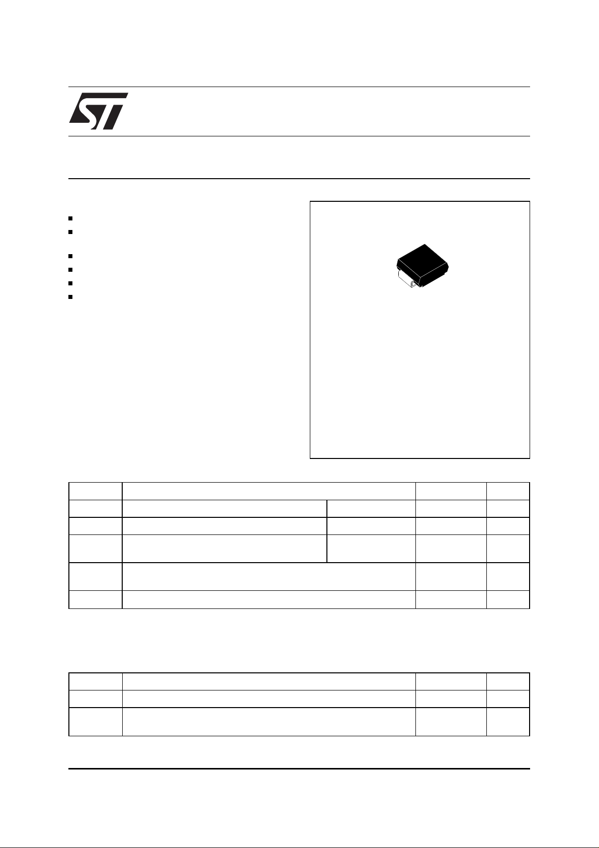
SMA J 188A -TR,CA -TR
TRANSIL
SMA
(JEDEC D0214 AC)
TM
ABSOL UTE M AXIMU M RA TIN GS (T
amb
= 25°C)
Symbol Parameter Value Unit
P
PP
P Power dissipation on infinite heatsink T
I
FSM
T
stg
T
j
T
L
Note 1
: For a surge greater than the maximum valu es, the diode wil l fail in short-ci rcuit.
Peak pulse power dissipation (see note 1) Tj initial = T
°C3.3W
Non repetitive surge peak forward
current for unidirectional types
amb = 50
tp = 10ms
Tj initial = T
Storage temperature range
Maximum junction temperature
amb
amb
400 W
40 A
- 65 to + 175
150
Maximum lead temperature for soldering during 10 s. 260 °C
THERMAL RE SISTA NC ES
Symbol Parameter Value Unit
R
R
th (j-l)
th (j-a)
Junction to leads 30 °C/W
Junction to ambient on printed circuit on recommended pad
120 °C/W
layout
September 1998 Ed: 5A
°C
°C
1/5
Page 2
SMAJxxxA-TR, CA-TR
ELECTRICAL CHARACTERISTICS (T
Symbol Parameter
amb
= 25°C)
I
I
F
V
RM
V
BR
V
CL
I
RM
I
PP
α
T Voltage temperature coefficient
V
F
Unidirectional Mark. Bidirectional Mark. µAV VmAV A V A10
Stand-off voltage
Breakdown voltage
Clamping voltage
Leakage current @ V
Peak pulse current
Forward voltage drop
Types
RM
VV
CLVBR
I
@ VRMVBR @ IRVCL @ I
RM
V
RM
PPVCL
I
I
RM
PP
@ I
V
F
TC
α
PP
max min max max max typ
note2 10/1000µs 8/20µs note3 note4
-4
/°CpF
V
SMAJ5.0A-TR AE SMAJ5.0CA-TR AA 800 5.0 6 .4 10 9 .2 43.5 13.4 174 5.7 3500
SMAJ6.0A-TR DUB SMAJ6.0CA-TR DBB 800 6.0 6.7 10 10.3 38.8 13.7 170 5.9 3300
SMAJ6.5A-TR DUC SMAJ6.5CA-TR DBC 500 6.5 7.2 10 11.2 35.7 14.5 160 6.1 3100
SMAJ8.5A-TR DUH SMAJ8.5CA-TR DBH 10 8.5 9 .44 1 14.4 27.7 18.6 124 7.3 2000
SMAJ10A-TR AX SMAJ10CA-TR AC 5 10 11.1 1 17 23.5 21.7 106 7.8 1550
SMAJ12A-TR DUK SMAJ12CA-TR DBK 5 12 13.3 1 19.9 20.1 25.3 91 8.3 1325
SMAJ13A-TR BG SMAJ13CA-TR BH 1 13 14.4 1 21.5 18.6 27.2 85 8.4 1200
SMAJ15A-TR BM SMAJ15CA-TR AJ 1 15 16.7 1 24.4 16.4 32.5 71 8.8 975
SMAJ18A-TR DUQ SMAJ18CA-TR DBQ 1 18 20 1 29.2 13.7 39.3 59 9.2 800
SMAJ20A-TR DUR SMAJ20CA-TR DBR 1 20 22.2 1 32.4 12.3 42.8 54 9.4 725
SMAJ22A-TR DUS SMAJ22CA-TR DBS 1 22 24.4 1 35.5 11.2 48.3 48 9.6 625
SMAJ24A-TR DUT SMAJ24CA-TR DBT 1 24 26.7 1 38.9 10.3 50 46 9.6 600
SMAJ26A-TR DUU SMAJ26CA-TR DBU 1 26 28.9 1 42.1 9.5 53.5 43 9.7 575
SMAJ28A-TR CG SMAJ28CA-TR CH 1 28 31.1 1 45.4 8.8 59 39 9.8 510
SMAJ30A-TR CK SMAJ30CA-TR CL 1 30 33.3 1 48.4 8.3 64.3 36 9.9 480
SMAJ33A-TR CM SMAJ33CA-TR CN 1 33 36.7 1 53.3 7.5 69.7 33 10.0 450
SMAJ40A-TR DUZ SMAJ40CA-TR DBZ 1 40 44.4 1 64.5 6.2 84 27 10.1 370
SMAJ43A-TR EUA SMAJ43CA-TR EBA 1 43 47.8 1 69.4 5.7 91 25 10.2 350
SMAJ48A-TR CX SMAJ48CA-TR CY 1 48 53.3 1 77.4 5.2 100 23 10.3 320
SMAJ58A-TR EUF SMAJ58CA-TR EBF 1 58 64.4 1 93.6 4.3 121 19 10.4 270
SMAJ70A-TR EUI SMAJ70CA-TR EBI 1 70 77.8 1 113 3.5 146 16 10.5 230
SMAJ85A-TR EUL SMAJ85CA-TR EBL 1 85 94.4 1 137 2.9 178 13 10.6 200
SMAJ100A-TR EUN SMAJ100CA-TR EBN 1 100 111 1 162 2.5 212 11 10.7 170
SMAJ130A-TR EUQ SMAJ130CA-TR EBQ 1 130 144 1 209 1.9 265 9 10.8 145
SMAJ154A-TR EUT SMAJ154CA-TR EBT 1 154 171 1 246 1.6 317 7 10.8 125
SMAJ170A-TR SR SMAJ170CA-TR SS 1 170 189 1 275 1.4 353 6.5 10.8 120
SMAJ188A-TR EUV SMAJ188CA-TR EBV 1 188 209 1 328 1.4 388 6 10.8 110
2/5
100
%I
PP
10 s
50
0
PULSE WAVEFORM 10/1000 s
1000 s
t
Note 2 :
Pulse test : tp < 50 ms.
Note 3 :
Note 4 :
capacitance value is divided by 2.
VBR = αT * (T
∆
VR = 0 V, F = 1 MHz. For bidirectional types,
- 25) * VBR(25°C).
amb
Page 3

SMAJxxxA-TR, CA-TR
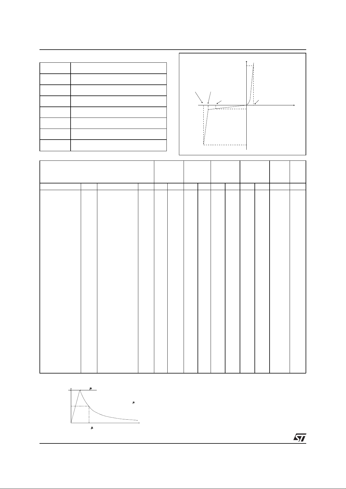
Fig 1: Peak power dissipation versus initial
junction temperature.
Ppp[Tj initial]/Ppp[Tj initial=25°C]
1.1
1.0
0.9
0.8
0.7
0.6
0.5
0.4
0.3
0.2
0.1
0.0
0 25 50 75 100 125 150 175
Tj initial(°C)
Fig 3: Clamping voltage versus peak pulse current
(Tj initial=25° C)
Exponential waveform tp=20µs & tp=1ms.
Ipp(A)
200.0
100.0
SMAJ5.0A,CA
SMAJ13A,CA
tp=20µs
SMAJ26A,CA
Fig 2: Peak pulse power versus exponential pulse
duration (Tj initial=25°C).
Ppp(W)
5000
1000
tp(ms)
100
0.01 0.10 1.00 10.00
10.0
tp=1ms
SMAJ58A,CA
SMAJ188A,CA
1.0
V (V)
CL
0.1
1 10 100 500
Fig 4-1: Capacitance versus reverse applied
voltage (typical values) (SMAJxxA).
C(pF)
5000
SMAJ5.0A
F=1MHz
1000
SMAJ13A
SMAJ26A
SMAJ58A
100
10
1 10 100 200
SMAJ188A
V (V)
R
Fig 4-2: Capacitance versus reverse applied
voltage (typical values) (SMAJxxCA).
C(pF)
2000
1000
100
10
1
1 10 100 200
SMAJ5.0CA
SMAJ13CA
SMAJ26CA
SMAJ58CA
SMAJ188CA
V (V)
F=1MHz
R
3/5
Page 4

SMAJxxxA-TR, CA-TR
Fig 5: Peak forward voltage drop versus peak
forward current (typical values).
I (A)
FM
10.00
1.00
0.10
0.01
0.4 0.5 0.6 0.7 0.8 0.9 1.0 1.1 1.2 1.3 1.4
Tj=125°C
Tj=25°C
V (V)
FM
Fig 7: Thermal resistance junction to ambient
versus copper surface under each lead
(printed circuit board FR4 e(C u)=35µm).
Rth(j-a) (°C/W)
140
130
120
110
100
90
80
70
60
50
40
012345
S(Cu)(cm²)
Fig 6: Relative variation of thermal impedance
junction to ambient versus puls e dur ation.
Zth(j-a)/Rth(j-a)
1.00
0.10
0.01
1E-2 1E-1 1E+0 1E+1 1E+2 5E+2
tp(s)
Fig 8: Relative variation of leakage current versus
junction temperature.
I [Tj] / I [Tj=25°C]
RR
2E+3
1E+3
V 8.5V
BR ≥
1E+2
1E+1
V < 8.5V
1E+0
BR
Tj(°C)
1E-1
0 25 50 75 100 125 150
4/5
Page 5

ORDER CODE
SMAJxxxA-TR, CA-TR
SURFACE MOUNT
400 WATTS
SM A J 85 C A - TR
TAPE & REEL
BIDIRECTIONAL
No suffix : Unidirectional
STAND OFF VOLTAGE
MARKING : Logo, Date Code, Type Code, Cathode Band (for unidirectional types only).
PACKAGE MECHANICAL DAT A
SMA (Plastic)
REF.
E1
Millimeters Inches
Min. Max. Min. Max.
DIMENSIONS
A1 1.90 2.70 0.075 0.106
D
A2 0.05 0.20 0.002 0.008
b 1.25 1.65 0.049 0.065
E
A1
C
L
A2
b
c 0.15 0.41 0.006 0.016
E 4.80 5.60 0.189 0.220
E1 3.95 4.60 0.156 0.181
D 2.25 2.95 0.089 0.116
L 0.75 1.60 0.030 0.063
FOOTPRINT DIMENSIONS (Millimeter)
SMA Plastic.
Weight
= 0.068 g
Packaging
1.45 1.45
2.40
1.65
Information furnished is believed to be accurate and reliable. However, STMicroelectronics assumes no responsibility for
the consequences of use of such information nor for any infringement of patents or other rights of third parties which may
result from its use. No license is granted by implication or otherwise under any patent or patent rights of STMicroelectronics.
Specifications mentioned in this publi cation are subject to change without notice. This p ublication supersede s and replaces
all information previo usly supplied.
STMicroelectronics products are not authorized for use as critical components in life support devices or systems without
express written approval of STMicroe lectronics.
The ST logo is a registered trademark of STMicro electroni cs
© 1998 STMicroelectronics - Printed in Italy - All rights reserved.
STMicroelectronics GROUP OF COMPANIES
Australia - Brazil - Canada - China - France - Germany - Italy - Japan - Korea - Malaysia - Malta - Mexico - Morocco -
The Netherlands - Singapore - Spain - Sweden - Switzerland - Taiwan - Thailand - United Kingdom - U.S.A.
: standard packaging is in tape and r eel.
5/5
 Loading...