

Page 1
Transient Voltage Suppression Diodes
Bi-directional
Surface Mount – 600W > SMA6L series
SMA6L Series
Uni-directional
Agency Approvals
AGENCY AGENCY FILE NUMBER
E230531
Maximum Ratings and Thermal Characteristics
(TA=25°C unless otherwise noted)
Parameter Symbol Value Unit
Peak Pulse Power Dissipation at
TA=25ºC by 10/1000µs Waveform
(Fig.2)(Note 1), (Note 2)
Power Dissipation on Infinite Heat
Sink at T
Peak For ward Surge Current, 8.3ms
Single Half Sine Wave (Note 3)
Maximum Instantaneous Forward
Voltage at 25A for Unidirectional
Only
Operating Junction and Storage
Temperature Range
Typical Thermal Resistance Junction
to Lead
Typical Thermal Resistance Junction
to Ambient
Notes:
1. Non-repetitive current pulse, per Fig.4 and derated above T
2. Mounted on 5.0x5.0mm copper pad to each terminal.
3. Measured on 8.3ms single half sine wave or equivalent square wave for unidirectional
device only.
=50°C
A
P
PPM
P
M(AV)
I
FSM
V
, T
T
J
R
uJL
R
uJA
F
-55 to 150 °C
STG
=25ºC per Fig. 3.
A
600 W
3 W
60 A
3.5V V
35 °C/W
200 °C/W
RoHS
Description
The SMA6L series is designed specifically to protect
sensitive electronic equipment from voltage transients
induced by lightning and other transient voltage events.
SMA low profile package has the same electronical
performance as the SMB package but with low height
profiles (1.1mm) in the industry.
Features
• SMA low prole package:
less than 1.1 mm
• Same power as standard
SMB devices (600 W)
• Footprint compatibility
with standard SMA and
SMB products (easy to
layout)
• Typical failure mode is
short from over-specified
voltage or current
• Whisker test is conducted
based on JEDEC
JESD201A per its table 4a
and 4c
• IEC-61000-4-2 ESD
15kV(Air), 8kV (Contact)
• ESD protection of data
lines in accordance with
IEC 61000-4-2 (IEC801-2)
• EFT protection of data
lines in accordance with
• Low inductance, excellent
clamping capability
• Fast response time:
typically less than 1.0ns
from 0 Volts to V
BR
min
• Built-in strain relief
• Glass passivated junction
• Typical I
less than 1µA
R
above 12V
• High temperature
soldering: 260°C/40
seconds at terminals
•
VBR @TJ= VBR@25°C × (1+αT
x (T
- 25))
J
(αT: Temperature Coefcient)
• Meet MSL level1, per
J-STD-020, LF maximum
peak of 260°C
• Matte tin lead–free plated
• Halogen free and RoHS
compliant
IEC 61000-4-4 (IEC801-4)
Applications
TVS devices are ideal for the protection of I/O Interfaces,
V
bus and other vulnerable circuits used in Telecom,
CC
Computer, Industrial and Consumer electronic applications.
Additional Information
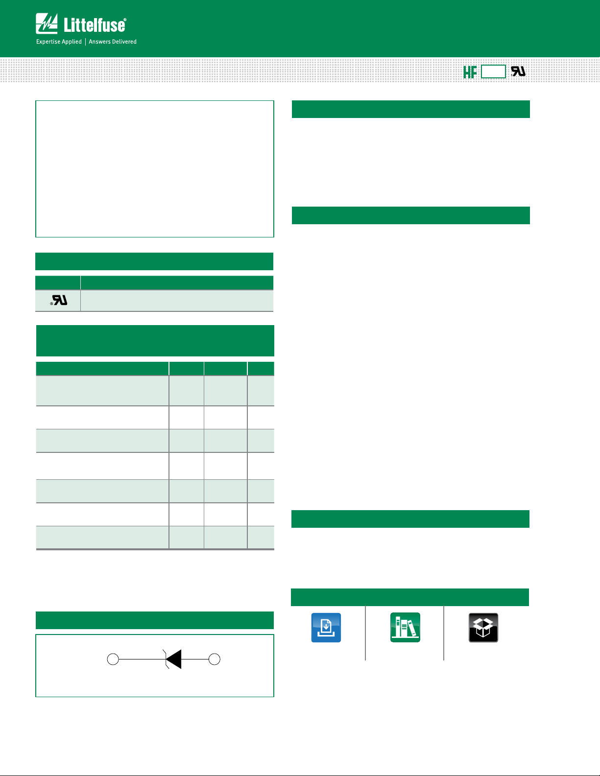
Functional Diagram
Cathode
Uni-directional
Anode
Datasheet
Resources
Specifications are subject to change without notice.
Samples
© 2014 Littelfuse, Inc.
Revised: 01/20/14
Page 2
Transient Voltage Suppression Diodes
Surface Mount – 600W > SMA6L series
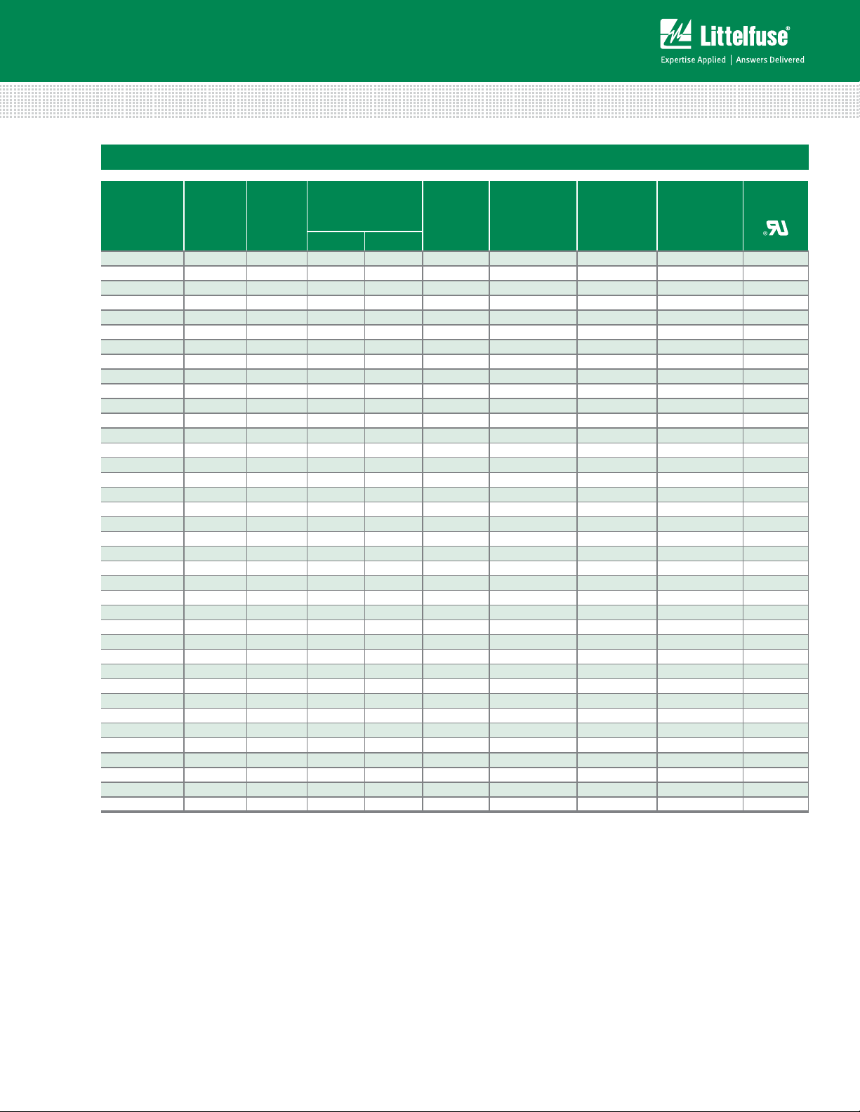
Electrical Characteristics (T
Part
Number
(Uni)
SMA6L5.0A AE 5.0 6.40 7.00 10 9.2 65.3 800 X
SMA6L6.0A AG 6.0 6.67 7.37 10 10.3 58.3 800 X
SMA6L6.5A AK 6.5 7.22 7.98 10 11. 2 53.6 500 X
SMA6L7.0A AM 7. 0 7.78 8.60 10 12.0 50.0 200 X
SMA6L7.5A AP 7. 5 8.33 9.21 1 12.9 46.6 10 0 X
SMA6L8.0A AR 8.0 8.89 9.83 1 13.6 44.2 50 X
SMA6L8.5A AT 8.5 9.44 10.40 1 14.4 41.7 20 X
SMA6L9.0A AV 9.0 10.00 11.10 1 15.4 39.0 10 X
SMA6L10A AX 10.0 11.10 12.30 1 1 7. 0 35.3 5 X
SMA6L11A AZ 11. 0 12.20 13.50 1 18.2 33.0 1 X
SMA6L12A BE 12.0 13.30 14.70 1 19.9 30.2 1 X
SMA6L13A BG 13.0 14.40 15.90 1 21.5 28.0 1 X
SMA6L14A BK 14.0 15.60 17.20 1 23.2 25.9 1 X
SMA6L15A BM 15.0 16.70 18.50 1 24.4 24.6 1 X
SMA6L16A BP 16.0 17.80 19.70 1 26.0 23.1 1 X
SMA6L17A BR 1 7. 0 18.90 20.90 1 27.6 21.8 1 X
SMA6L18A BT 18.0 20.00 22.10 1 29.2 20.6 1 X
SMA6L20A BV 20.0 22.20 24.50 1 32.4 18.6 1 X
SMA6L22A BX 22.0 24.40 26.90 1 35.5 16.9 1 X
SMA6L24A BZ 24.0 26.70 29.50 1 38.9 15.5 1 X
SMA6L26A CE 26.0 28.90 31.90 1 42.1 14.3 1 X
SMA6L28A CG 28.0 31.10 34.40 1 45.4 13.3 1 X
SMA6L30A CK 30.0 33.30 36.80 1 48.4 12.4 1 X
SMA6L33A CM 33.0 36.70 40.60 1 53.3 11. 3 1 X
SMA6L36A CP 36.0 40.00 44.20 1 58.1 10.4 1 X
SMA6L40A CR 40.0 44.40 49.10 1 64.5 9.3 1 X
SMA6L43A CT 43.0 47.80 52.80 1 69.4 8.7 1 X
SMA6L45A CV 45.0 50.00 55.30 1 72.7 8.3 1 X
SMA6L48A CX 48.0 53.30 58.90 1 77.4 7. 8 1 X
SMA6L51A CZ 51.0 56.70 62.70 1 82.4 7. 3 1 X
SMA6L54A RE 54.0 60.00 66.30 1 87.1 6.9 1 X
SMA6L58A RG 58.0 64.40 71.20 1 93.6 6.5 1 X
SMA6L60A RK 60.0 66.70 73.70 1 96.8 6.2 1 X
SMA6L64A RM 64.0 71.10 78.60 1 103.0 5.9 1 X
SMA6L70A RP 70.0 77.80 86.00 1 113.0 5.3 1 X
SMA6L75A RR 75.0 83.30 92.10 1 121.0 5.0 1 X
SMA6L78A RT 78.0 86.70 95.80 1 126.0 4.8 1 X
SMA6L85A RV 85.0 94.40 104.00 1 137.0 4.4 1 X
Marking
Code
=25°C unless otherwise noted)
A
Reverse
Stand off
Voltage V
(Volts)
Breakdown
Voltage V
(Volts) @ I
R
MIN MAX
pp
Maximum
Reverse
Leakage I
@ V
R
(µA)
R
Agency
Approval
Test
BR
T
Current
I
T
(mA)
Maximum
Clamping
Voltage V
@ Ipp
(V)
C
Maximum
Peak Pulse
Current I
(A)
© 2014 Littelfuse, Inc.
Specifications are subject to change without notice.
Revised: 01/20/14
Page 3
Transient Voltage Suppression Diodes
0.1
1
10
100
0.0000010.00001 0.0001 0.001
t
d
-Pulse Width (sec.)
0.2x0.2" (5.0x5.0mm)
Copper Pad Area
P
PPM
-Peak Pulse Power (kW)
Voltage Transients
Time
Voltage Across TVS
Current Through TVS
Voltage or Current
Surface Mount – 600W > SMA6L series
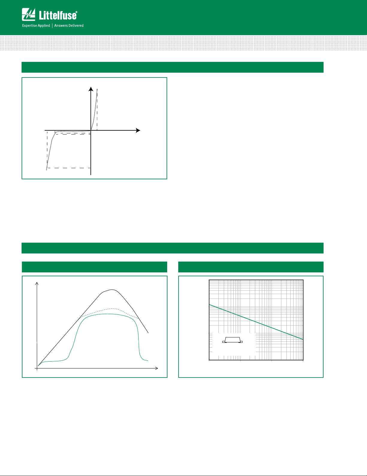
I-V Curve Characteristics
Uni-directional
BR
V
Vc
VR
IR
VF
IT
Ipp
P
Peak Pulse Power Dissipation -- Max power dissipation
PPM
V
Stand-off Voltage -- Maximum voltage that can be applied to the TVS without operation
R
V
Breakdown Voltage -- Maximum voltage that flows though the TVS at a specified test current (IT)
BR
V
Clamping Voltage -- Peak voltage measured across the suppressor at a specified Ippm (peak impulse current)
C
I
Reverse Leakage Current -- Current measured at V
R
V
Forward Voltage Drop for Uni-directional
F
V
R
Ratings and Characteristic Curves (T
=25°C unless otherwise noted)
A
Figure 1 - TVS Transients Clamping Waveform
Figure 2 - Peak Pulse Power Rating Curve
continues on next page.
Specifications are subject to change without notice.
© 2014 Littelfuse, Inc.
Revised: 01/20/14
Page 4
Transient Voltage Suppression Diodes
T
A
1
10
100
1000
10000
1.0 10.0100.01000.0
Cj (pF)
Tj=25ºC
f=1.0MHz
Vsig=50mVp-p
Uni-directional V=0V
Uni-directional @V
R
VBR - Reverse Breakdown Voltage (V)
Surface Mount – 600W > SMA6L series
Ratings and Characteristic Curves (T
=25°C unless otherwise noted) (Continued)
A
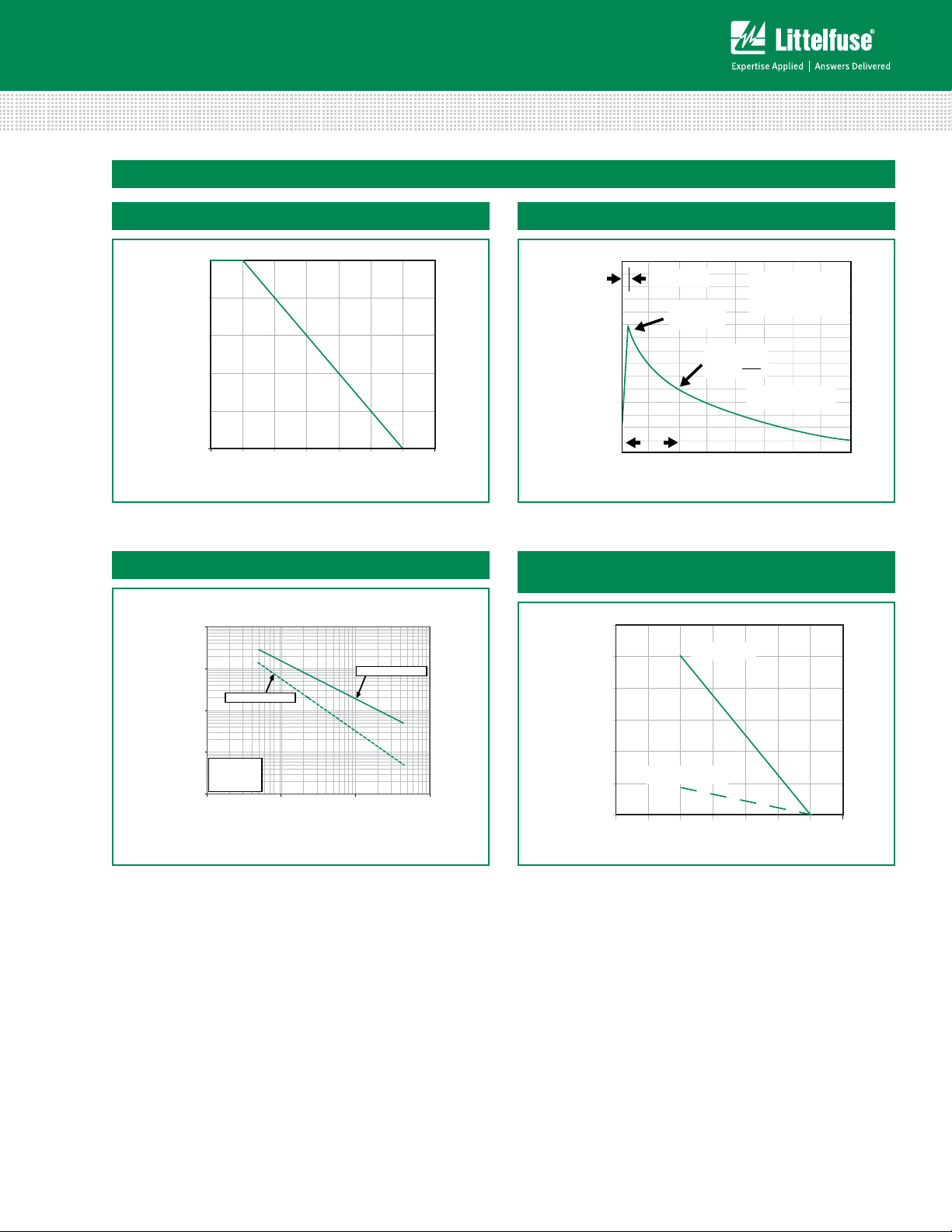
Figure 3 - Pulse Derating Curve
100
)
PP
80
60
) or Current (I
PP
40
Derating in Percentage %
20
Peak Pulse Power (P
0
0255075 100 125 150 175
-Ambient temperature (ºC)
Figure 5 - Typical Junction Capacitance
Figure 4 - Pulse Waveform
150
RSM
100
50
- Peak Pulse Current, % I
PPM
I
0
tr=10µsec
Peak Value
I
PPM
t
d
0
1.0 2.0 3.0 4.0
Half Value
I
I
PPM
( )
TJ=25°C
Pulse Width(td) is defined
as the point where the peak
current decays to 50% of I
PPM
2
10/1000µsec. Waveform
as defined by R.E.A
PPM
t-Time (ms)
Figure 6 - Steady State Power Dissipation Derating
Curve
3.6
3.0
RuJA=RuJL
2.4
1.8
1.2
0.6
, Steady State Power Dissipation (W)
M(AV)
P
0
RuJA=200°C/W
0255075 100 125 150 175
TA - Ambient Temperature (ºC)
© 2014 Littelfuse, Inc.
Specifications are subject to change without notice.
Revised: 01/20/14
Page 5
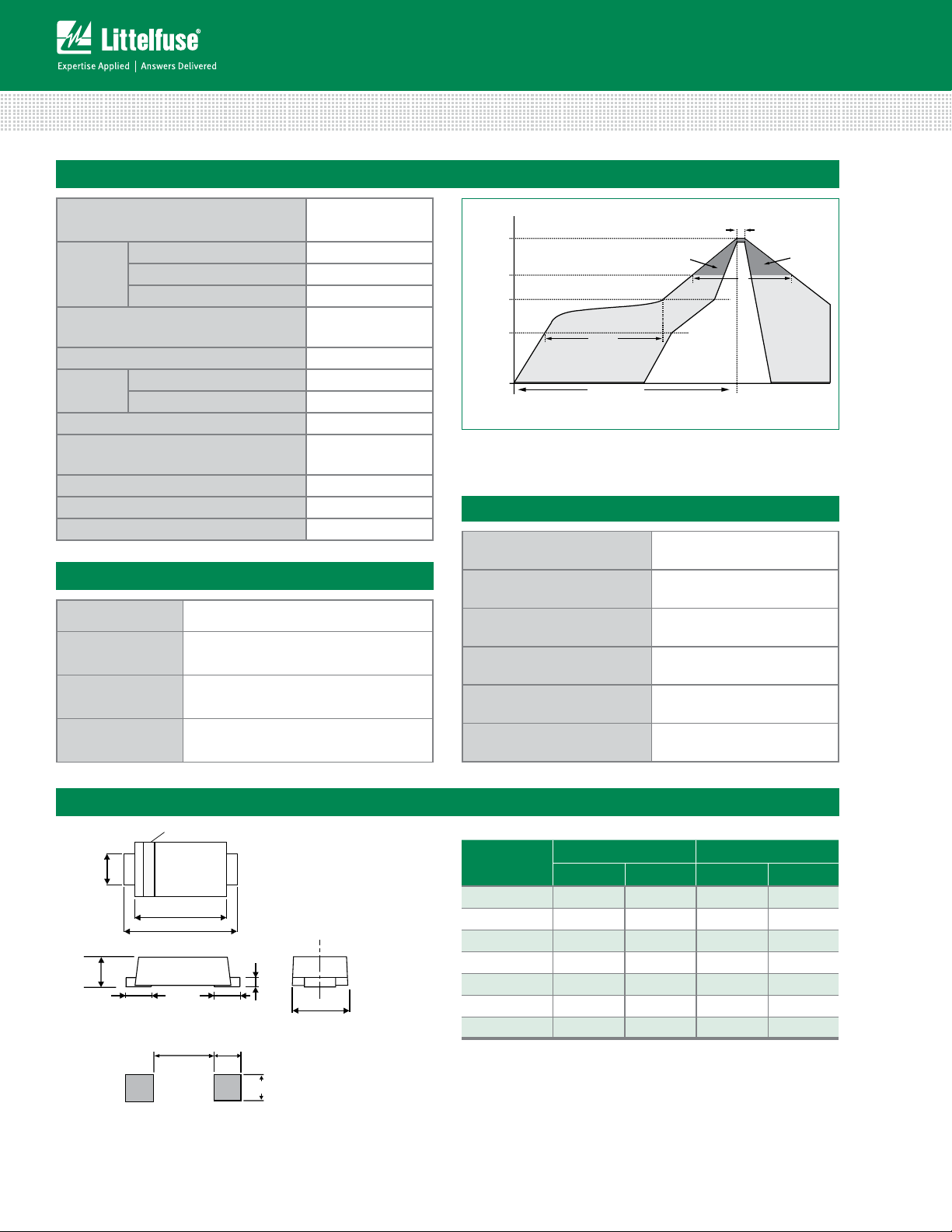
Soldering Parameters
Transient Voltage Suppression Diodes
Surface Mount – 600W > SMA6L series
Reflow Condition Lead–free assembly
Pre Heat
- Temperature Min (T
- Temperature Max (T
) 150°C
s(min)
) 200°C
s(max)
- Time (min to max) (ts) 60 – 180 secs
Average ramp up rate (Liquidus Temp
(T
) to peak
L
to TL - Ramp-up Rate 3°C/second max
T
S(max)
Reflow
- Temperature (TL) (Liquidus) 217°C
- Time (min to max) (ts) 60 – 150 seconds
Peak Temperature (TP) 260
Time within 5°C of actual peak
Temperature (t
)
p
3°C/second max
+0/-5
°C
20 – 40 seconds
Ramp-down Rate 6°C/second max
Time 25°C to peak Temperature (T
) 8 minutes Max.
P
Do not exceed 280°C
Physical Specifications
Weight 0.002 ounce, 0.061 gram
Case
JEDEC DO-221AC Molded Plastic over
glass passivated junction
t
T
P
Ramp-up Critical Zone
T
L
T
s(max)
T
s(min)
Temperature (T)
25˚C
t
s
Preheat
t 25˚C to Peak
Time (t)
p
t
L
Ramp-down
Environmental Specifications
High Temp. Storage JESD22-A103
HTRB JESD22-A108
Temperature Cycling JESD22-A104
MSL JEDEC-J-STD-020, Level 1
T
T
to
L
P
Polarity Color band denotes cathode except Bipolar
Terminal
Matte Tin-plated leads, Solderable per
JESD22-B102
Dimensions
Cathode Band
C
A
B
G
E
3.12 (0.123) 1.20 (0.047)
Mounting Pad Layout
E
F
D
1.52 (0.060)
H3TRB JESD22-A101
RSH JESD22-B106
Dimensions
Inches Millimeters
Min Max Min Max
A 0.156 0.181 3.950 4.600
B 0.189 0.220 4.800 5.600
C 0.049 0.069 1.250 1.750
D 0.088 0.116 2.250 2.950
E 0.030 0.059 0.750 1.500
F 0.005 0 .010 0.125 0.250
G 0.035 0.043 0.900 1. 10 0
Specifications are subject to change without notice.
© 2014 Littelfuse, Inc.
Revised: 01/20/14
Page 6
Transient Voltage Suppression Diodes
F
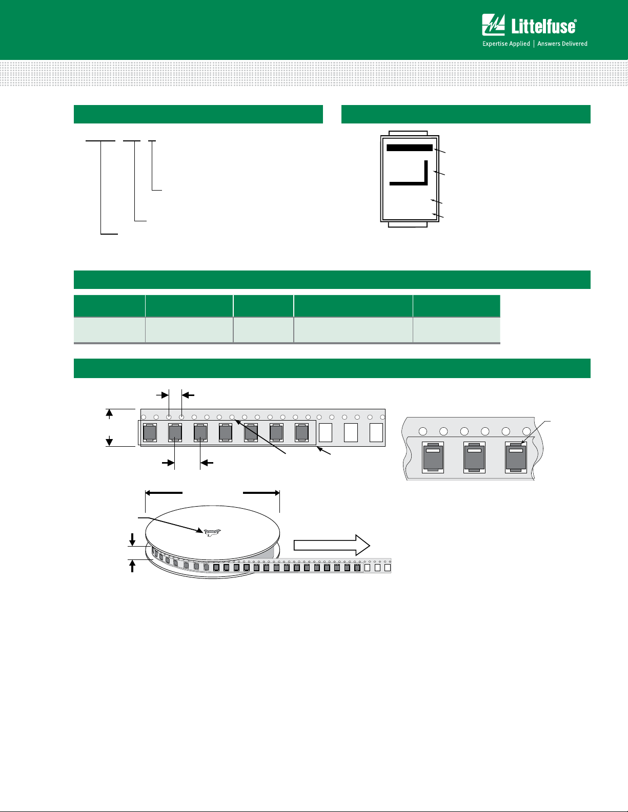
XX
YMXXX
Marking Code
Trace Code Marking
Y:Year Code
M: Month Code
XXX: Lot Code
Littelfuse Logo
Cathode Band
(for uni-directional products only)
0.157
Arbor Hole Dia.
Cathode
Surface Mount – 600W > SMA6L series
Part Numbering System Part Marking System
SMA6L xx A
5%
V
VOLTA GE TOLERANCE
BR
V
VOLTA GE
R
SERIES
Packaging
Part number
SMA6LxxA DO-221AC 3000 Tape & Reel – 12mm/7” tape EIA RS-481
Tape and Reel Specification
0.47
(12.0)
0.80 (20.2)
0.49
(12.5)
(4.0)
Component
Package
0.157
(4.0)
7.0 (178)
Quantity
Packaging
Option
0.059
(1.5)
Dimensions are in inches
(and millimeters).
Direction of Feed
DIA
Cover tape
Packaging
Specification
© 2014 Littelfuse, Inc.
Specifications are subject to change without notice.
Revised: 01/20/14
 Loading...