

Page 1
SM8750AV
NIPPON PRECISION CIRCUITS INC.
Data Jitter Measurement IC
OVERVIEW
The SM8750AV is a data jitter measurement CMOS LSI for adaptive control.
FEATURES
■
RDCLK and DATA signal phase difference to
voltage converter (75mV/ns (typ) coefficient)
■
RDCLK duty auto-adjust function (rising edge
reference)
■
DATA signal delay auto-adjust function (independently adjusted on rising and falling edges)
■
Offset auto-calibration function
■
3-wire serial interface mode control
■
Sleep function
■
Single 5V supply
■
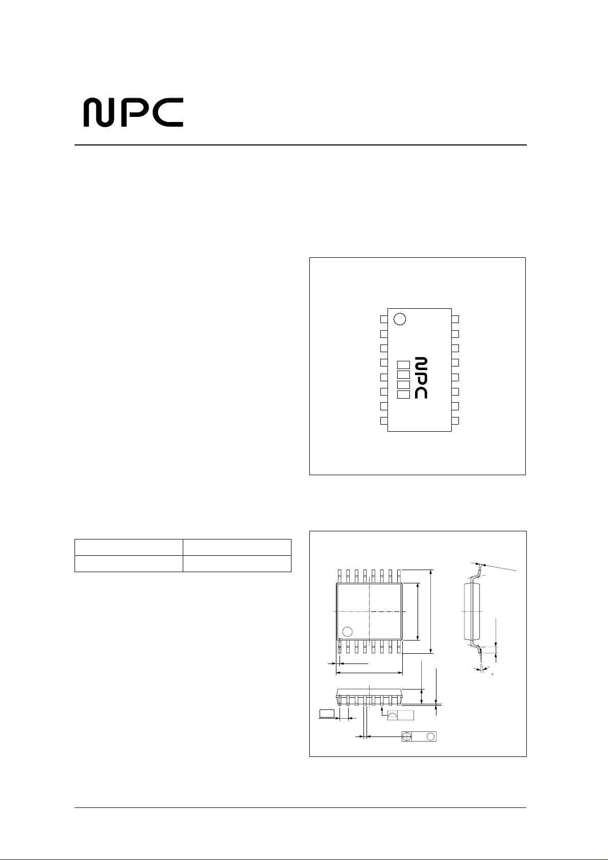
16-pin VSOP
APPLICATIONS
■
Optical disc equipment
• CD-R
• CD-RW
• DVD-RAM
• Others
■
Control/governing equipment
PINOUT
START
DATA
CALMON
RDCLK
LIMIT
SENB
SCLK
SDATA
PACKAGE DIMENSIONS
1
8
Top view
87
50A
V
16
9
VDD
TVOUT
VREF2
RCP
RDUTY
RDATAF
RDATAR
GND
ORDERING INFORMATION
De vice Pack ag e
SM8750AV 16-pin VSOP
Unit: mm
0.65
0.275typ
5.1 ± 0.2
0.22
+ 0.1
− 0.05
0.10
4.4 ± 0.2
1.15 ± 0.1
0.12
6.4 ± 0.2
0.10 ± 0.05
M
0 to 10
0.15
+ 0.10
− 0.05
0.5 ± 0.2
NIPPON PRECISION CIRCUITS—1
Page 2
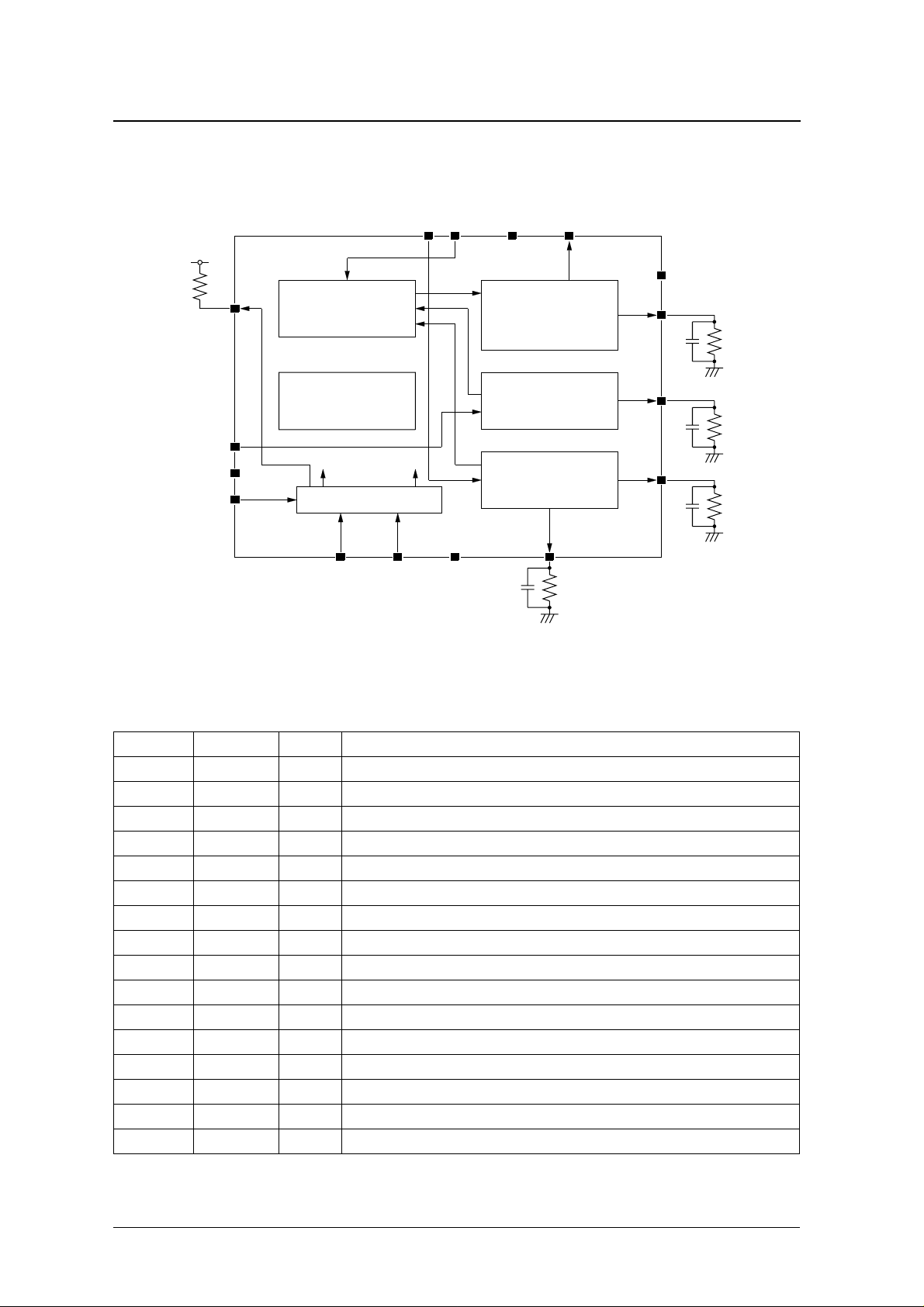
BLOCK DIAGRAM
SM8750AV
VDD
47k
CALMON
RDCLK
LIMIT
SENB
Phase comparator
Automatic regulation
controller
to each block
Serial interface
SCLK
SDATA GND RDATAR
STARTDATA
VDD TVOUT
Charge pump
(phase difference to
voltage converter)
Duty correction
Delay correction
output buffer
39k
VREF2
RCP
33k
RDUTY
22k
RDATAF
39k
PIN DESCRIPTION
Number Name I/O Description
1 STAR T I Measurement start control. Phase difference to voltage conversion starts on the falling edge.
2 DATA I Tw o-valued signal input
3 CALMON O Internal calibration state signal monitor output. N-channel open drain. Active when calibrated.
4 RDCLK I PLL clock input
5 LIMIT I TVOUT output voltage-limit control voltage input
6 SENB I Serial interface: enable signal input
7 SCLK I Serial interface: clock signal input
8 S DATA I/O Serial interface: data signal input/acknowledge signal output. N-channel open drain.
9 G ND – Ground
10 R D ATAR O D ATA rising edge: delay adjust circuit reference-current setting resistor connection
11 RD ATAF O DATA falling edge: delay adjust circuit reference-current setting resistor connection
12 RDUTY O RDCLK duty adjust circuit reference-current setting resistor connection
13 R C P O Phase difference to voltage converter coefficient reference-current setting resistor connection
14 VREF2 I 2V reference voltage input
15 TV O U T O Phase difference to voltage conver ter output
16 VD D – 5V supply
NIPPON PRECISION CIRCUITS—2
Page 3
+
−
−
−
°
° C
−
SM8750AV
SPECIFICATIONS
Absolute Maximum Ratings
GND = 0V
Parameter Symbol Rating Unit
Supply voltage range V
Input voltage range V
Storage temperature range T
Po w er dissipation P
Recommended Operating Conditions
GND = 0V
DD
IN
stg
D
0.5 to 7.0 V
0.5 to V
0.5 V
DD
40 to 125
250 m W
C
Parameter Symbol Rating Unit
Supply voltage (specifications guaranteed) V
Supply voltage (operation guaranteed) V
Reference voltage input V
Operating temperature range T
DC Electrical Characteristics
V
= 5V ± 5%, GND = 0V, T
DD
Parameter Symbol Condition
Current consumption
HIGH-level logic input voltage
L O W -level logic input voltage
HIGH-level logic input current
L O W -level logic input current
1
2
2
2
2
SD ATA, CALMON logic output voltage V
VREF2 input current I
1. 39k Ω resistor connected between RDATAR and GND
39k Ω resistor connected between RDATAF and GND
22k Ω resistor connected between RDUTY and GND
resistor connected between RCP and GND
33k Ω
60MHz RDCLK input frequency
7.5MHz DATA input frequency
200kHz STAR T input frequency
0ns DATA and RDCLK phase difference
Serial interface not operating.
2. Pins STA RT, DATA, RDCLK, SENB, SCLK, SDATA.
= 0 to 70 ° C
a
I
DD1
I
DD2
V
IH
V
IL
I
IH
I
IL
OL
REF
Normal operating mode – 9.0 13.0
Sleep mode – 0.5 0.7
V
= V
IN
DD
V
= GND
IN
I
= 10mA – – 1.0 V
OL
VRFE2 = 2V – 50 100 µA
DD
DD
REF2
opr
4.75 to 5.25 V
4.5 to 5.5 V
1.89 to 2.11 V
0 to 70
Rating
Unit
min typ max
mA
2.4 – – V
– – 0.6 V
––3µA
3– –µA
NIPPON PRECISION CIRCUITS—3
Page 4

×
−
×
×
−
×
SM8750AV
Phase Difference to Voltage Converter Characteristics
V
= 5V ± 5%, GND = 0V, T
DD
= 0 to 70 ° C
a
Parameter Condition
RDCLK input frequency
Phase difference to voltage converter
coefficient 1
Phase difference to voltage converter
coefficient 2
Phase difference to voltage converter
coefficient 3
Co n ver ter coefficient relative accura cy See note.
Co n ver ter coefficient relative accura cy See note.
Output offset voltage After VREF2 reference calibration – – ±25 mV
C o nver ter voltage settling time
C o nver ter voltage reset time
Output load regulation I
HIGH-level output voltage range LIMIT pin voltage reference +0.15 – +0.45 V
L O W-level output voltage range 0.8 – – V
Output voltage droop – – 1 mV/µs
STA R T-DATA setup time
3
FCG = LOW – 58.38 70
FCG = HIGH – 29.19 35
Nor mal operation, FCG = LO W 50 75 100 mV/ns
Converter coefficient measurement mode,
FCG = LOW
Nor mal operation, FCG = HIGH 25 37.5 50
Converter coefficient measurement mode,
FCG = HIGH
1
2
Time from measurement object DATA
edge to final set value ± 0.5%
Time from STA RT signal rising edge to
final reset value ± 1mV
= 0.5mA – – 2 0 m V
L
S TA R T signal rising edge to DATA signal
edge
min typ max
25 37.5 5 0
12.5 18.75 25 mV/ns
––±5%
––±5%
– – 0.75 µs
––3µs
1T – – ns
Rating
Unit
MHz
mV/ns
1. {[(conver ter coefficient 2)
2. {[(conver ter coefficient 3)
3. T = RDCLK cycle time
2 / (converter coefficient 1)]
2 / (converter coefficient 2)]
1}
1}
100
100
Auto-adjust Characteristics
V
= 5V ± 5%, GND = 0V, T
DD
Parameter Condition
Maximum DATA edge delay adjust range – 29 – ns
Minimum DATA edge delay adjust range – 12.5 – ns
Maximum RDCLK pulsewidth adjust range
Minimum RDCLK pulsewidth adjust range – 3 – ns
Maximum RDCLK pulsewidth adjust range
Minimum RDCLK pulsewidth adjust range – 4 – ns
Auto-adjustment time After CS = HIGH, until settling – 5 8 m s
RCP voltage Co n verter coefficients set – 1 – V
HIGH-level RDATAR/RDATAF voltage Minimum DATA delay – 1.92 – V
LOW -level RDATAR/RDATAF voltage Maximum DATA delay – 0.69 – V
HIGH-level RDUTY voltage Minimum RDCLK pulsewidth – 1.88 – V
LOW-level RDUTY voltage Maximum RDCLK pulsewidth – 0.24 – V
= 0 to 70 ° C
a
FCG = LOW
FCG = HIGH
Rating
min typ max
–15–ns
–28–ns
Unit
NIPPON PRECISION CIRCUITS—4
Page 5

Serial Interface Characteristics
SM8750AV
Parameter Symbol
Unit
min typ max
Rating
SCLK pulse cycle time t
SCLK HIGH-level pulsewidth t
SCLK LOW-level pulsewidth t
SENB setup time t
SENB hold time t
S DATA setup time t
S DATA hold time t
ACK setup time
ACK hold time
1
1
SENB interval t
cySCK
whSCK
wlSCK
sSEN
hSEN
sSDA
hSDA
t
sACK
t
hACK
inSEN
100 – – ns
40 – – ns
40 – – ns
20 – – ns
40 – – ns
15 – – ns
15 – – ns
0–20ns
––50ns
100 – – ns
1. SDATA output signal (ACK) acknowledge output (N-channel open drain), receive data is valid, LOW-level output, 15pF SDATA load capacitance.
tinSEN
SENB
tsSEN twhSCK twlSCK
tcySCK
thSEN
SCLOCK
SDATA
Controller
SDATA port
tsSDA
thSDA
bit0 bit1 bit15
LSB MSB
tsACK
thACK
ACK
High impedance
NIPPON PRECISION CIRCUITS—5
Page 6

FUNCTIONAL DESCRIPTION
Serial Interface
SM8750AV
×
×
−
The SM8750AV has a dedicated serial interface port
over which data can be written and the various oper-
bit configuration are shown in table 1, and the data
bits are described in table 2.
ating modes can be controlled. The port address and
Table 1. Port address and bit configuration
Bit number
15
(msb)
TEST1 TEST0 CSDIS CS SP POLAR GMES FCG
1413121110987654321
Data Address
LOW HIGH HIGH HIGH HIGH HIGH
: Don’t care.
Table 2. Data bit description
Bit Description Default
TEST[1:0] Test mode setting L O W:LOW (normal operation)
CSDIS Auto-adjust disable L OW (enabled)
C S A uto-adjust start L O W (wait)
SP Sleep mode settings LO W (normal operation)
POLAR
DATA edge settings for phase measurement
Polarity setting for c o nv e r ter coefficient measurement
LOW
(falling edge)
(1T discharge)
0
(lsb)
×
GMES Converter coefficient measurement mode setting L O W (normal operation)
FCG
RDCLK pulsewidth auto-adjust mode
Phase difference to voltage converter coefficient switching
LOW
(minimum pulsewidth)
(maximum converter coefficient)
Table 3. GMES and POLAR operating modes
GMES POLAR Operating mode
L O W L OW D ATA signal falling edge and RDCLK rising edge phase difference conversion
LOW HIGH DATA signal rising edge and RDCLK rising edge phase difference conversion
HIGH LOW Output converter voltage for phase difference equivalent to
HIGH HIGH Output converter voltage for phase difference equivalent to +0.5T
Serial data comprising 16 bits is input with the LSB
first. Valid data is read in on the 16th rising edge of
the SCLK input. On the next SCLK falling edge, the
SDATA N-channel open drain is turned ON and
SDATA goes LOW, performing the function of an
acknowledge signal.
If 15 or less SCLK rising edge pulses occur during
up to the point when SENB goes LOW is ignored
and the internal port data is not updated. If 17 or
more SCLK rising edge pulses occur, the received
data is latched in the internal port on the 16th rising
edge and the acknowledge signal is output on the
next falling edge. The acknowledge signal is held
constant until SENB goes LOW again.
0.5T
the interval when SENB is HIGH, the data received
NIPPON PRECISION CIRCUITS—6
Page 7

Phase Difference to Voltage Converter
SM8750AV
The phase difference to voltage converter circuit
takes the converts the phase difference between the
RDCLK rising edge and the DATA signal to a voltage. When START goes LOW, the phase difference
between the first active DATA signal edge, where the
active edge polarity is determined by the serial interface bit POLAR, and the next RDCLK rising edge is
converted to a voltage signal. The converted voltage
signal is output on TVOUT while START is LOW,
START
RDCLK
DATA
START−DATA set up time
Internal charge signal
Internal discharge signal
TVOUT output
VREF2
and is reset to the VREF2 reference level when
START goes HIGH again.
The START signal must go LOW for a minimum
interval of 1 RDCLK cycle before any DATA signal
edge to be converted, regardless of the number of
DATA signal edges. If the START interval is shorter
than 1 cycle, there is a possibility that the next edge
might be misinterpreted as the conversion object.
Phase difference
Conversion voltage
Reset
VREF2
Figure 1. Converter operation timing (POLAR = LOW, DATA leading phase)
START
RDCLK
DATA
Internal charge signal
Internal discharge signal
TVOUT output
Figure 2. Converter operation timing (POLAR = LOW, DATA lagging phase)
START−DATA set up time
VREF2
Phase difference
Conversion voltage
Reset
VREF2
NIPPON PRECISION CIRCUITS—7
Page 8

SM8750AV
Converter Coefficient Measurement Mode
When the serial interface bit GMES is set HIGH,
converter coefficient measurement mode is invoked.
In this mode, a voltage equivalent to a phase difference of ±0.5T, determined by the POLAR input bit,
is output on TVOUT. Internally, the difference in
START
RDCLK
Internal charge signal
Internal discharge signal
TVOUT output
VREF2
Figure 3. Converter coefficient measurement mode timing (POLAR = LOW)
pulsewidth between the charge/discharge signals is
±1T, where the charge pump circuit capacitance is
double the capacitance during normal operation in
order to generate outputs equivalent to phase differences of ±0.5T.
Conversion voltage
(corresponds to −0.5T)
Reset
VREF2
START
RDCLK
Internal charge signal
Internal discharge signal
TVOUT output
Figure 4. Converter coefficient measurement mode timing (POLAR = HIGH)
VREF2
Conversion voltage
(corresponds to +0.5T)
Reset
VREF2
NIPPON PRECISION CIRCUITS—8
Page 9

Auto-adjust Function
SM8750AV
When the serial interface bit CS is set HIGH, the
auto-adjust function starts and operates on the
objects in the sequence described below. In the autoadjust sequence cycle, the RDCLK pulsewidth and
DATA delay are set to approximately the center of
the adjustment range.
1. Charge pump circuit and output buffer offset
cancellation
An identical 0.5T signal is added to the
charge/discharge signals and the output on
TVOUT is calibrated to an output voltage of
VREF2.
2. RDCLK pulsewidth
Signals equivalent to the RDCLK HIGH-level
pulsewidth and LOW-level pulsewidth are added
to the internal charge/discharge signals, and the
RDCLK pulsewidths are adjusted to recover a
TVOUT output voltage of VREF2.
3. DATA rising edge delay
The phase difference between the RDCLK rising
edge and DATA rising edge is converted to a
voltage, and the RDCLK rising edge delay is
adjusted to recover a TVOUT output voltage of
VREF2.
4. DATA falling edge delay
The phase difference between the RDCLK rising
edge and DATA falling edge is converted to a
voltage, and the RDCLK rising edge delay is
adjusted to recover a TVOUT output voltage of
VREF2.
The CALMON calibration monitor output is high
impedance during the auto-adjust sequence interval.
When auto-adjustment is completed, the CALMON
N-channel open drain turns ON and CALMON goes
LOW, and the CS bit is cleared to LOW.
When the serial interface bit CSDIS is set HIGH, the
auto-adjustment result is disabled, and the external
inputs on RDCLK and DATA are input to the phase
comparator without adjustment. If CS and CSDIS
are both simultaneously set HIGH, the auto-adjust
sequence still takes place but that the result is disabled as soon as the sequence is completed.
When power is switched ON, the auto-adjust
sequence is enabled, and the adjusted values are
approximately in the center of the corresponding
adjustment range.
Sleep Mode
When the serial interface bit SP is set HIGH, sleep
mode is invoked. In this mode, all circuits other than
the power-ON detection circuit and serial interface
circuit are shutdown to reduce current consumption.
When operation transfers from sleep mode to normal
operating mode, the auto-adjust settings from the
most recent auto-adjust cycle are restored.
Power-ON Reset
When power is switched ON, a built-in power-ON
reset circuit sets all serial interface bit settings to
LOW (factory preset default), and the auto-adjust
circuit settings are set to the middle of the corresponding adjustment range.
Test Mode
When the serial interface bit TEST1 or TEST0 is set
HIGH, a test mode is invoked. In these modes, the
phase comparator input signals and internal
Table 4. Test modes
TEST1 TEST0 CALMON TVOUT
LO W L OW No rmal operation Nor mal operation
LOW HIGH Internal charge signal Internal discharge signal
HIGH LOW Phase comparator RDCLK signal Phase comparator DATA signal
charge/discharge signals are output on CALMON
and TVOUT.
NIPPON PRECISION CIRCUITS—9
Page 10

SM8750AV
NIPPON PRECISION CIRCUITS INC. reserves the right to make changes to the products described in this data sheet in order to
improve the design or performance and to supply the best possible products. Nippon Precision Circuits Inc. assumes no responsibility for
the use of any circuits shown in this data sheet, conveys no license under any patent or other rights, and makes no claim that the circuits
are free from patent infringement. Applications for any devices shown in this data sheet are for illustration only and Nippon Precision
Circuits Inc. makes no claim or warranty that such applications will be suitable for the use specified without further testing or modification.
The products described in this data sheet are not intended to use for the apparatus which influence human lives due to the failure or
malfunction of the products. Customers are requested to comply with applicable laws and regulations in effect now and hereinafter,
including compliance with export controls on the distribution or dissemination of the products. Customers shall not export, directly or
indirectly, any products without first obtaining required licenses and approvals from appropriate government agencies.
NIPPON PRECISION CIRCUITS INC.
4-3, Fukuzumi 2-chome
Koto-ku, Tokyo 135-8430, Japan
NIPPON PRECISION CIRCUITS INC.
Telephone: 03-3642-6661
Facsimile: 03-3642-6698
NC9916AE 2000.07
NIPPON PRECISION CIRCUITS—10
 Loading...