

Page 1
SM8706A
NIPPON PRECISION CIRCUITS INC.
Clock Generator for DVD Players
OVERVIEW
The SM8706A is a clock generator IC that generates 3 clocks with 6 outputs from a 36.8640MHz master clock
for application in DVD players. The SM8706A has 2 built-in PLL circuits that together with a crystal oscillator
can generate the 384fs and 768fs audio system clocks, 27MHz and 54MHz video system clocks, and
16.9344MHz and 33.8688MHz signal processor system clocks required for a DVD player. The SM8706A also
supports the 44.1kHz and 48kHz sampling frequencies, and the sampling frequency can be switched while the
device is operating.
FEATURES
■
36.8640MHz master clock (internal PLL reference
clock)
■
Generated clocks
• Video system output: 27MHz, 54MHz
• Audio system output: 384fs, 768fs
• Signal processor system output: 16.9344MHz,
33.8688MHz
■
Supported sampling frequency fs: 44.1/48kHz
■
Low jitter output: 40ps (typ, 1-sigma, 25pF load)
■
Supply voltage: 3.3V ± 0.3V
■
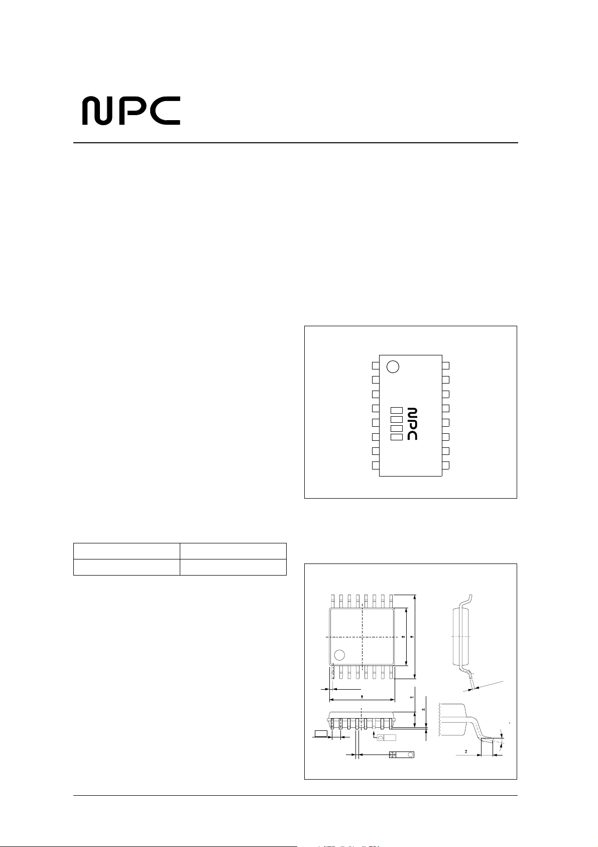
16-pin VSOP package
APPLICATIONS
PINOUT
(Top view)
VDD1
1
16
VSS1
MO1
8706AV
MO2
VDD2
VSS2
XTI
XTO AO1
8
9
CE
SO2
FSEL
SO1
VDD3
VSS3
AO2
■
DVD players
■
DVD car navigation system
ORDERING INFORMATION
Device Package
SM8706AV 16-pin VSOP
PACKAGE DIMENSIONS
(Unit: mm)
Weight: 0.07g
4.4 0.2
6.4 0.2
0.275typ
5.1 0.2
1.15 0.1
0.10 0.05
0.65
0.22
+ 0.1
- 0.05
0.10
0.12
M
0.5 0.2
0.15
+ 0.1
- 0.05
0 to 10
NIPPON PRECISION CIRCUITS—1
Page 2
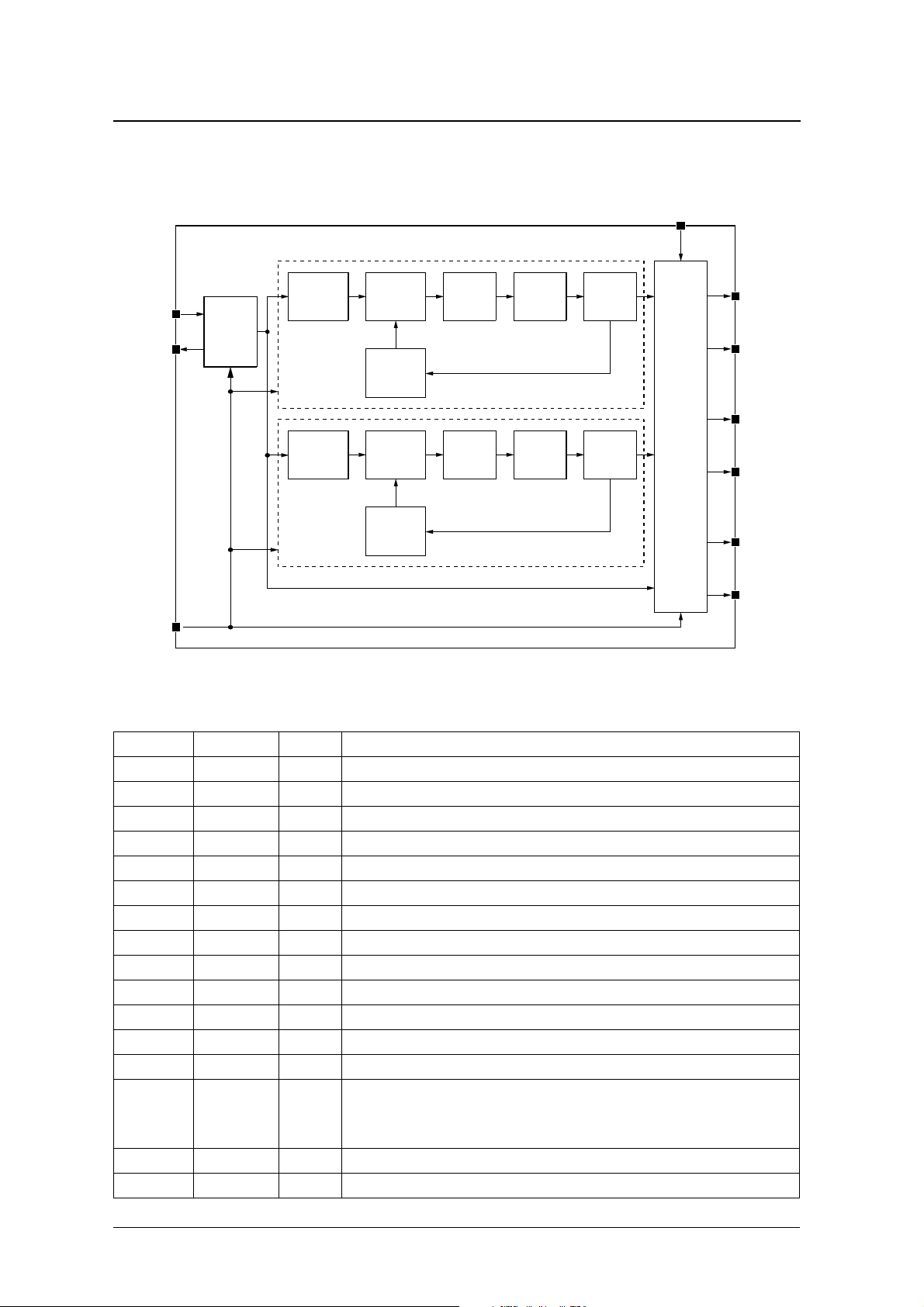
BLOCK DIAGRAM
SM8706A
FSEL
XTI
XTO
CE
X'tal
OSC
PIN DESCRIPTION
Reference
Divider 0
(PLL 0)
Reference
Divider 1
(PLL 1)
Phase
Detector 0
Loop
Divider 0
Phase
Detector 1
Loop
Divider 1
Charge
Pump 0
Charge
Pump 1
LPF 0 VCO 0
LPF 1 VCO 1
Control
Logic
AO1
AO2
SO1
SO2
MO1
MO2
Number Name I/O Description
1 VDD1 – Supply 1 for digital block
2 VSS1 – Ground 1 for digital block
3 MO1 O Video system output 1 (27MHz fixed)
4 MO2 O Video system output 2 (54MHz fixed)
5 VDD2 – Supply 2 for analog block
6 VSS2 – Ground 2 for analog block
7 XTI I Crystal oscillator connection or external clock input
8 XTO O Crystal oscillator connection
9 AO1 O Audio system output 1 (384fs output)
10 AO2 O Audio system output 2 (768fs output)
11 VSS3 – Ground 3 for digital block
12 VDD3 – Supply 3 for digital block
13 SO1 O Signal processor system output 1 (16.9344MHz fixed)
Sampling frequency select
14 FSEL I
15 SO2 O Signal processor system output 2 (33.8688MHz fixed)
16 CE I Chip enable (HIGH = Enable, LOW = Disable)
FSEL = HIGH: fs = 48kHz
FSEL = LOW: fs = 44.1kHz
(with internal pull-up resistor, Schmitt-trigger input)
NIPPON PRECISION CIRCUITS—2
Page 3
−
−
+
−
+
−
° C
° C
−
−
−
SM8706A
Note: Unless otherwise noted, VDD applies to VDD1, VDD2, and VDD3. Similarly, VSS applies to VSS1,
VSS2, and VSS3.
SPECIFICATIONS
Absolute Maximum Ratings
Parameter Symbol Condition Rating Unit
Supply voltage range V
Supply voltage deviation
Input voltage range V
Output voltage range V
Power dissipation P
Storage temperature range T
DD1
V
V
V
DD1
DD1
DD2
, V
DD2
– V
– V
– V
OUT
, V
DD3
,
DD2
,
DD3
DD3
IN
D
stg
0.3 to 6.5 V
± 0.1 V
0.3 to V
0.3 to V
0.3 V
DD
0.3 V
DD
165 mW
55 to 125
Recommended Operating Conditions
V
= V
SS1
= V
SS
Parameter Symbol Condition
Supply voltage ranges
Output load capacitance 1 C
Output load capacitance 2 C
Master clock frequency f
Operating temperature range T
1. The supply voltage is defined relative to V
2. The supply voltages applied on VDD1, VDD2, and VDD3 should be derived from a common supply source.
SS2
1, 2, 3
= V
= 0V unless otherwise noted.
SS3
V
, V
DD2
XTAL
opr
SS
L1
L2
= 0V
, V
DD3
MO1, SO1, SO2 outputs – – 25 pF
All outputs excluding MO1,
SO1, SO2, XTO
When using crystal oscillator – 36.8640 – MHz
DD1
Rating
min typ max
Unit
+ 3.0 – + 3.6 V
– – 15 pF
– 40 – + 85
3. If the supply voltages on VDD1, VDD2, and VDD3 are from different sources, they should be applied simultaneously. The SM8706A may be damaged
if the supply voltage timing is different.
DC Electrical Characteristics
f
= 36.8640MHz, V
XTAL
Parameter Symbol Condition
Current consumption I
HIGH-level input voltage V
LOW-level input voltage V
HIGH-level input current
LOW-level input current
1
1
HIGH-level input current I
LOW-level input current I
HIGH-level output voltage V
LOW-level output voltage V
1. FSEL and CE pins have Schmitt-trigger input and built-in pull-up resistor.
= 3.0V ± 0.3V, V
DD
DD
IH
IL
I
IH1
I
IL1
IH2
IL2
OH
OL
= 0V, Ta = – 40 to 85 ° C unless otherwise noted.
SS
min typ max
V
= 3.3V, Ta = 25 ° C, fs = 48kHz,
DD
Crystal oscillator, no load on all
–3545mA
outputs
0.8 V
FSEL, CE, XTI, V
FSEL, CE, V
FSEL, CE, V
XTI, V
= V
IN
XTI, V
= 0V – 40 –
IN
= 3.3V
DD
= V
IN
DD
= 0V – 100 –
IN
DD
All outputs excluding XTO,
I
= − 2mA
OH
All outputs excluding XTO,
I
= 2mA
OL
DD
– – 0.2 V
––1µA
– – 40 µA
0.4 – – V
V
DD
– – 0.4 V
Rating
Unit
––V
DD
V
µA
µA
NIPPON PRECISION CIRCUITS—3
Page 4

AC Electrical Characteristics
f
= 36.8640MHz, V
XTAL
= 3.0V ± 0.3V, V
DD
SM8706A
= 0V, Ta = – 40 to 85 ° C unless otherwise noted.
SS
µ
Parameter Symbol Condition
Unit
min typ max
Rating
External input clock frequency
Output clock rise time
Output clock fall time
Output clock jitter
3
Output clock duty cycle
Settling time
Power-up time
2
2,4
1
f
2
2
t
(1-sigma)
2
XTI, applies to external clock input use only – 36.8640 – MHz
XTI
MO1, SO1, SO2, C
between V
t
r
Outputs excluding MO1, SO1, SO2, and XTO,
C
= 15pF, transition between V
L
and V
= 0.8V
OH
MO1, SO1, SO2, C
between V
t
f
Outputs excluding MO1, SO1, SO2, and XTO,
C
= 15pF, transition between V
L
and V
= 0.2V
OL
MO1, SO1, SO2, Ta = 25 ° C, C
0.5V
jitter
DD
Outputs excluding MO1, SO1, SO2, and XTO,
Ta = 25 ° C, C
MO1, SO1, SO2, Ta = 25 ° C, C
0.5V
Dt
DD
Outputs excluding MO1, SO1, SO2, and XTO,
Ta = 25 ° C, C
t
All outputs excluding XTO – – 1
S
t
All outputs excluding XTO – 1 5 ms
P
= 0.2V
OL
= 0.8V
OH
= 15pF, V
L
=15 pF, V
L
DD
DD
= 25 pF, transition
L
and V
and V
= 0.5V
O
= 0.5V
O
= 0.8V
OH
OL
= 0.2V
OL
OH
= 25pF, V
L
DD
= 25pF, V
L
DD
= 0.2V
= 0.8V
DD
= 25pF, transition
L
DD
DD
DD
DD
DD
=
O
– 2.0 –
– 2.0 –
– 2.0 –
– 2.0 –
–40–
–40–
=
O
45 50 55
45 50 55
ns
ns
ps
%
s
1. When using an external clock input, the XTI duty should be 50% with 3.3V clock signal amplitude level. The input signal voltage should not exceed the
absolute maximum rating, otherwise damage may occur.
2. The numeric values are measured values obtained using the circuit in Figure 1 and the NPC standard evaluation board.
3. The numeric values are measured values obtained using the circuit in Figure 2 and the NPC standard evaluation board.
4. This is the time, after the supply is turned ON from the OFF state, until the output clock reaches ± 0.1% of the specified frequency.
36.864MHz
DUT
DUT:Device under testing
Active Probe
(HP1152A)
Passive Probe
(HP10435A)
Figure 1. Measurement circuit 1
Oscilloscope
(Infinium
HP54845A)
Frequency &
Time Interval
Analyzer
(HP5371A)
36.864MHz
DUT
DUT:Device under testing
Figure 2. Measurement circuit 2
Active Probe
(HP54701A)
Oscilloscope
(HP54720D
+HP54721A)
NIPPON PRECISION CIRCUITS—4
Jitter
Measurement
System
(ASA, M1)
Page 5

SM8706A
FUNCTIONAL DESCRIPTION
36.8640MHz Master Clock
The SM8706A 36.8640MHz master clock circuit is configured, as shown in Figure 3, with the crystal oscillator
element connected between XTI (pin 7) and XTO (pin 8).
Alternatively, the 36.8640MHz master clock can be supplied from an external master clock input on XTI, as
shown in Figure 4.
If an external input clock on XTI is used, it is recommended that the frequency be 36.8640MHz, with 50%
duty, and 3.3V voltage amplitude level.
Furthermore, when using an external clock input, the input signal voltage should not exceed the absolute maximum rating, otherwise damage may occur.
C1
C2
C1, C2 = 5 to 33pF
External Clock
Open
XTI (Pin 7)
XTO (Pin 8)
Figure 3. Crystal oscillator connection
XTI (Pin 7)
XTO (Pin 8)
Oscillator
Oscillator
Internal
Circuits
Control
Logic
MO1 (Pin 3)
MO2 (Pin 4)
Internal
Circuits
Control
Logic
Figure 4. External clock input
MO1 (Pin 3)
MO2 (Pin 4)
NIPPON PRECISION CIRCUITS—5
Page 6

SM8706A
Sampling Frequency and Output Clock Frequency
The SM8706A sampling frequency fs can be switched between 44.1kHz when FSEL (pin 14) is LOW, and
48kHz when FSEL is HIGH. The audio outputs (AO1 and AO2) are a 384fs and 768fs frequency clock, respectively, where fs is determined by the setting on FSEL. In addition, the signal processor outputs (SO1 and SO2)
are a 16.9344MHz and 33.8688MHz frequency clock, respectively, derived from the master clock. The video
outputs (MO1 and MO2) are a 27MHz and 54MHz frequency clock, respectively, derived from the master
clock.
When CE (Pin16) is HIGH, the chip is enabled. When LOW, the chip is disabled. When disabled, all output go
LOW and all internal circuits stop operating. When CE goes LOW to HIGH, the chip moves from disabled to
enabled, the time taken until the output frequency clocks stabilize is a maximum of 5ms.
The SM8706A output clock frequencies that can be selected is shown in Table 1. The output clock response
timing relative to the CE setting is shown in Figure 5.
Table 1. Sampling frequency and output clock frequency (36.8640MHz master clock frequency)
FSEL
(Pin 14)
LOW 44.1
HIGH 48 18.4320 36.8640 16.9344 33.8688 27.0000 54.0000
LOW 44.1
HIGH 48
Sampling
frequency
fs [kHz]
AO1/AO2
SO1/SO2
MO1/MO2
CE
(Pin 16)
H
LLLLLLL
CE
AO1
(Pin 9)
16.9344 33.8688 16.9344 33.8688 27.0000 54.0000
AO2
(Pin 10)
Output clock frequency [MHz]
SO1
(Pin 13)
5ms
(max)
SO2
(Pin 15)
MO1
(Pin 3)
MO2
(Pin 4)
Figure 5. CE switching response
NIPPON PRECISION CIRCUITS—6
Page 7

SM8706A
Sampling Frequency Switching Settling Time
The clock output response timing when the sampling frequency fs is switched using FSEL is shown in Figure
6. The settling time ts for the audio output clock when switching the sampling frequency is 1µs maximum.
0.8V
FSEL
DD
0.2V
DD
tS
tS
AO1
AO2
MO1
MO2
SO1
SO2
fs = 44.1kHz fs = 44.1kHz
fs = 48kHz
27.0000MHz
/54MHz
16.9344MHz
/33.8688MHz
Figure 6. Output signal switching timing
NIPPON PRECISION CIRCUITS—7
Page 8

SM8706A
NIPPON PRECISION CIRCUITS INC. reserves the right to make changes to the products described in this data sheet in order to
improve the design or performance and to supply the best possible products. Nippon Precision Circuits Inc. assumes no responsibility for
the use of any circuits shown in this data sheet, conveys no license under any patent or other rights, and makes no claim that the circuits
are free from patent infringement. Applications for any devices shown in this data sheet are for illustration only and Nippon Precision
Circuits Inc. makes no claim or warranty that such applications will be suitable for the use specified without further testing or modification.
The products described in this data sheet are not intended to use for the apparatus which influence human lives due to the failure or
malfunction of the products. Customers are requested to comply with applicable laws and regulations in effect now and hereinafter,
including compliance with export controls on the distribution or dissemination of the products. Customers shall not export, directly or
indirectly, any products without first obtaining required licenses and approvals from appropriate government agencies.
NIPPON PRECISION CIRCUITS INC.
4-3, Fukuzumi 2-chome
Koto-ku, Tokyo 135-8430, Japan
Telephone: +81-3-3642-6661
NIPPON PRECISION CIRCUITS INC.
Facsimile: +81-3-3642-6698
http://www.npc.co.jp/
Email: sales
@npc.co.jp
NC0012AE 2000.12
NIPPON PRECISION CIRCUITS—8
 Loading...