

Page 1
SM8703AV
NIPPON PRECISION CIRCUITS INC.
Clock Generator for MPEG2 System
OVERVIEW
The SM8703AV is a 27 MHz master clock, 5-system output clock generator for MPEG2 system. It has 2 builtin PLLs that, with the addition of a single crystal oscillator element, can generate 384fs, 512fs and 768fs
clocks which are necessary for MPEG2 system, plus independent fixed-frequency 27 MHz and 33.8688 MHz
output clocks. Each output can stop unused output by using disable function, therefore, unnecessary radiation
can be suppressed. Also, visual and audio synchronous is not disrupted since each output frequency is kept in
the normal ratio. Supported sampling frequencies (fs) include 44.1 or 48 kHz.
FEATURES
■
27 MHz master clock (internal PLL reference
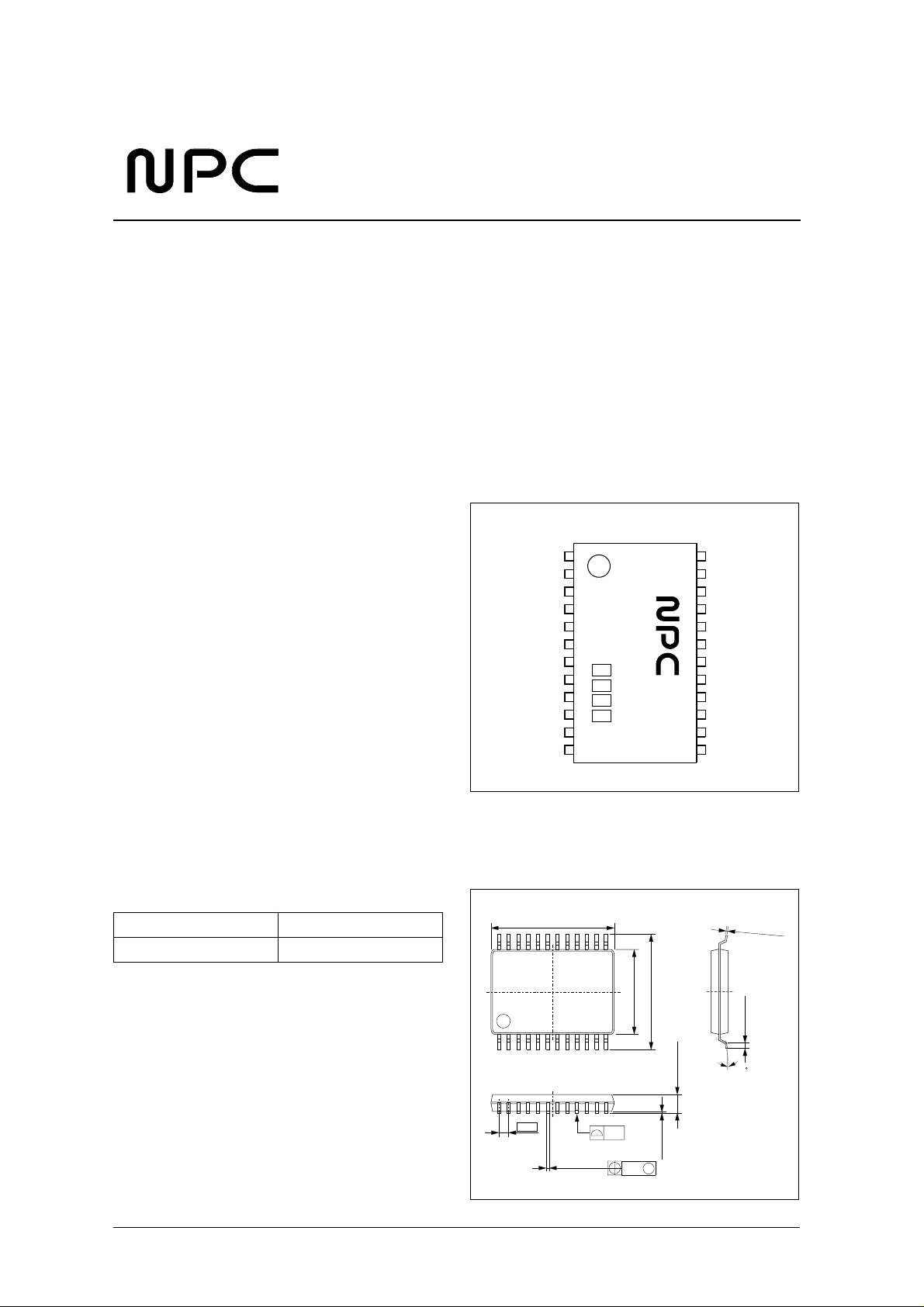
PINOUT
(T op V iew)
clock)
■
Generated clocks
• 27 MHz output
• 33.8688 MHz output
• 384fs output
• 512fs output
• 768fs output
■
Sampling frequency fs
• 44.1/48 kHz
■
Output disable function
■
Low jitter output: 100 ps (typ, 15pF load)
■
Supply voltage: 3.3 V
■
24-pin VSOP package
1
VDD
VSS
MO1
MCK
MLEN
VDDA
VSSA
XTI RSV
XTO
RSV
RSV
12 13
SO1
SM8703AV
24
MO2
FSEL/MDT
SO5
RSV
SO2
VDD1
VSS1
SO3
SO4
VDD2
VSS2
APPLICATIONS
■
DVD players
■
Set top box
■
MPEG2 system
ORDERING INFORMATION
De vice Pack ag e
SM8703AV 24-pin VSOP
PACKAGE DIMENSIONS
(Unit: mm)
7.8 ± 0.1
7.6 ± 0.2
5.6 ± 0.1
+ 0.2
0.65
0.22 − 0.05
0.1
+ 0.1
NIPPON PRECISION CIRCUITS—1
0.13
0.1 ± 0.1
M
1.25 − 0.1
0 to 10
0.15
0.5 ± 0.2
+
0.05
−
0.02
Page 2
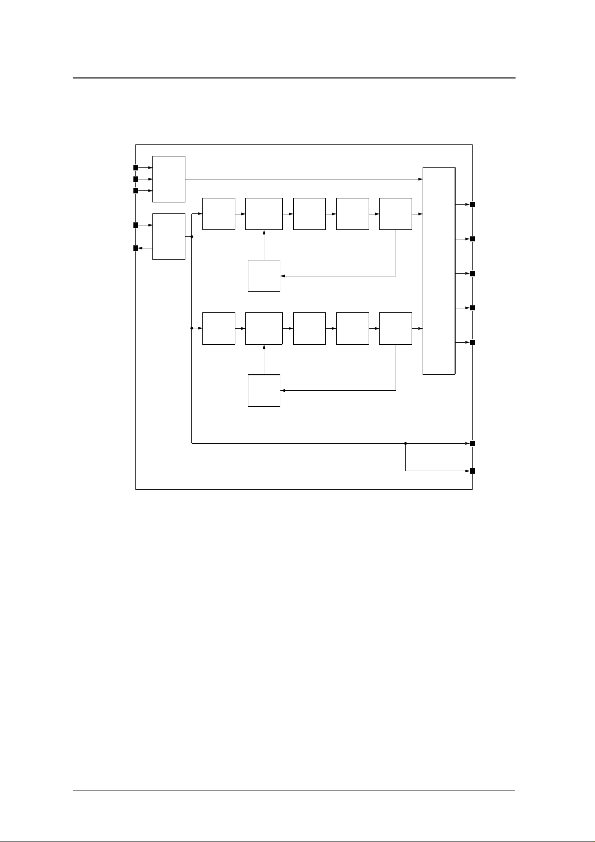
BLOCK DIAGRAM
SM8703AV
FSEL/MDT
MCK
MLEN
XTI
XTO
External
Interface
Oscillator
Divider0
Divider1
Phase
Comparator0
Divider0
Phase
Comparator1
Divider1
Charge
Pump0
Charge
Pump1
LPF0 VCO0
LPF1 VCO1
Divider
SO5
SO4
SO3
SO2
SO1
MO1
MO2
NIPPON PRECISION CIRCUITS—2
Page 3
SM8703AV
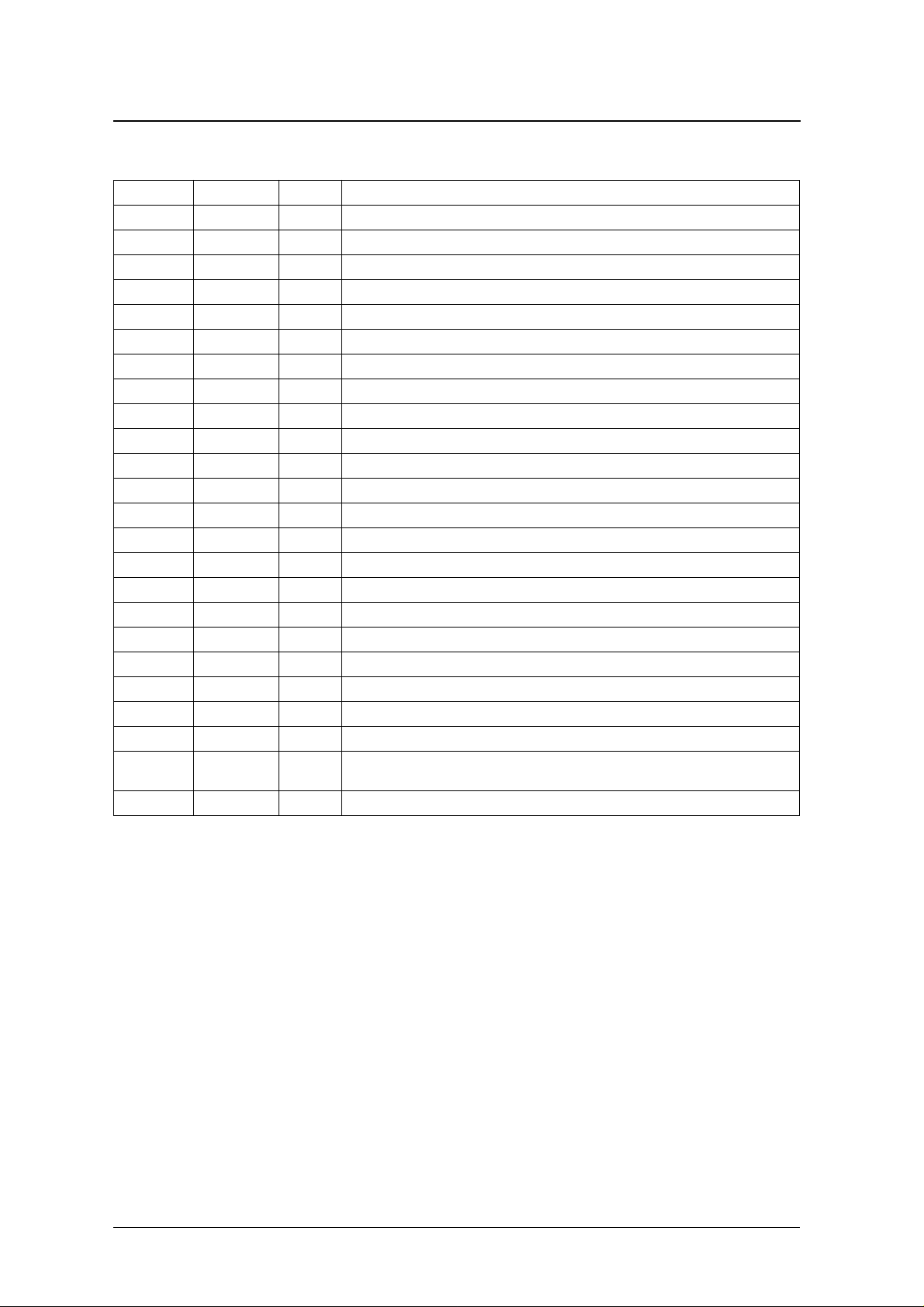
PIN DESCRIPTION
Number Name I/O Description
1 V DD – Po w er supply for Digital block
2 V SS – VSS for Digital block
3 MO1 O 27 MHz fixed-frequency output 1
1
4 MCK Ip
5 MLEN Ip
6 V DDA – Po w er supply for Analog block
7 VSSA – VSS for Analog block
8 XTI I Reference signal cr ystal oscillator element connection or external clock input
9 X T O O Re ference signal crystal oscillator element connection
10 R SV – Reserved (must be open)
11 R SV – Reserved (must be open)
12 SO1 O 33.8688 MHz fixed-frequency output
13 VSS2 – VSS for Output buffer
14 VDD2 – Power supply for Output buffer
15 SO 4 O 512fs output
16 SO 3 O 512fs output
17 R SV – Reserved (must be open)
18 VSS1 – VSS for Output buffer
19 VDD1 – Power supply for Output buffer
20 SO 2 O 384fs output
21 R SV – Reserved (must be open)
22 SO 5 O 768fs output
23 FSEL/MDT Ip
24 MO 2 O 27 MHz fixed-frequency output 2
1. Schmitt trigger input with internal pull-up resistor
Serial interface bit clock input
1
Serial interface latch enable input
Parallel mode: Sampling frequency select signal input
1
Ser ial mode: Control data input
NIPPON PRECISION CIRCUITS—3
Page 4
+
+
−
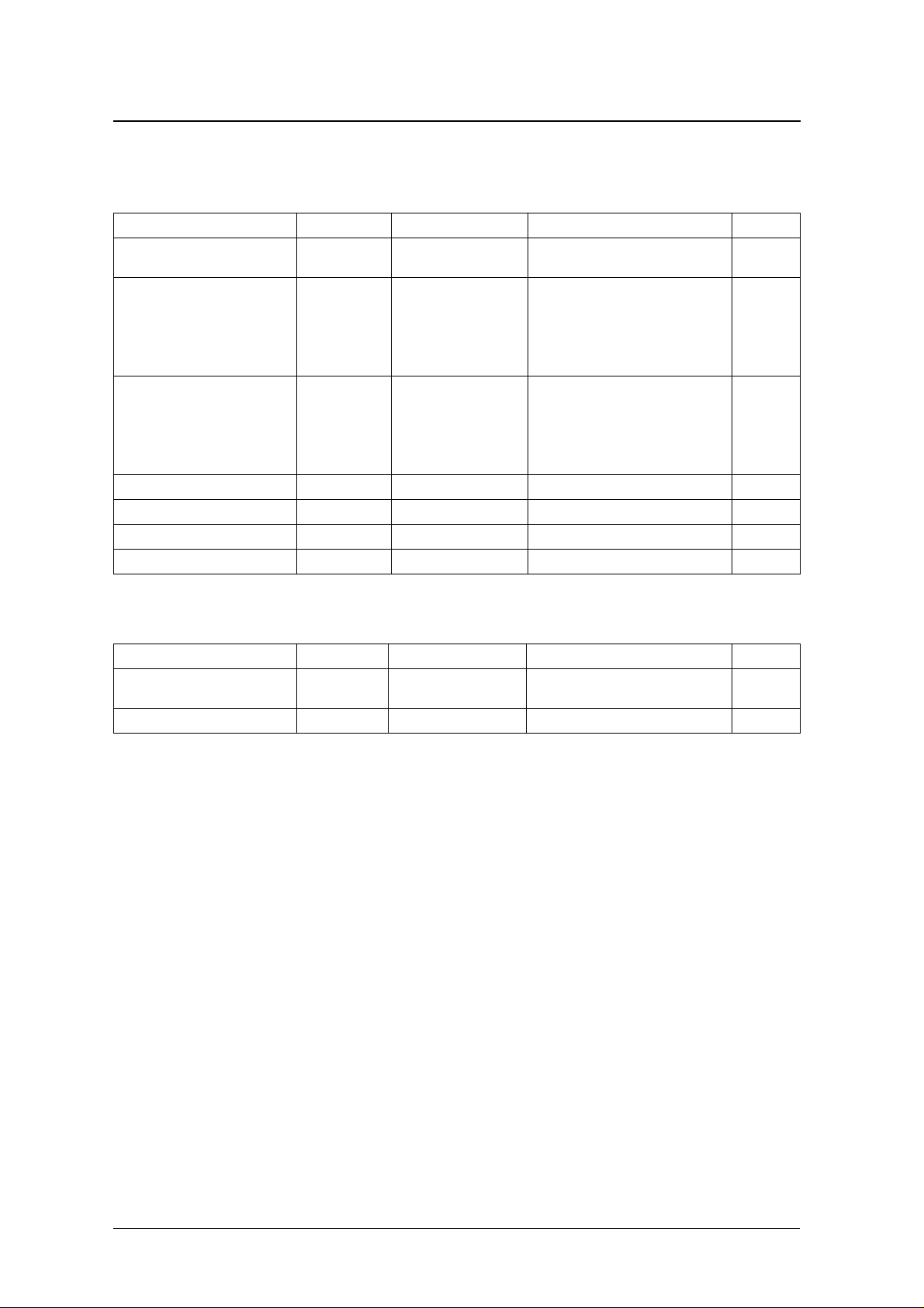
SPECIFICATIONS
Absolute Maximum Ratings
Parameter Symbol Condition Rating Unit
V
V
V
V
V
V
V
V
V
V
V
V
V
V
DDA
DD1
DDA
DDA
DDA
DD
DD
DD1
SSA
SSA
SSA
SS
SS
SS1
Supply voltage range
Supply voltage deviation
Ground voltage deviation
Input voltage range V
Output voltage range V
Po w er dissipation P
Storage temperature range T
−
−
−
° C
°
SM8703AV
, V
,
– V
– V
– V
– V
– V
– V
– V
– V
– V
– V
– V
– V
OUT
stg
, V
IN
D
DD
DD2
DD
DD1
DD2
DD1
DD2
DD2
SS
SS1
SS2
SS1
SS2
SS2
,
,
,
,
,
,
,
,
,
,
Digital inputs
Digital outputs
0.3 to 6.5 V
±0.1 V
±0.1 V
0.3 to V
0.3 to V
0.3 V
DD
0.3 V
DD
300 m W
55 to 125
Recommended Operating Conditions
Parameter Symbol Condition Rating Unit
V
, V
opr
,
DD
, V
DD2
Supply voltage ranges
V
DDA
DD1
Operating temperature range T
3.0 to 3.6 V
–40 to 85
C
NIPPON PRECISION CIRCUITS—4
Page 5

DC Electrical Characteristics
−
SM8703AV
°
−
−
−
External clock, T
= –40 to 85 ° C, V
a
Parameter Symbol Condition
Current consumption I
HIGH-level input voltage V
L O W -level input voltage V
HIGH-level input current I
L O W -level input current I
HIGH-level input current I
L O W -level input current I
HIGH-level output voltage V
L O W-level output voltage V
DD
IH
IL
IH1
IL1
IH2
IL2
OH
OL
AC Electrical Characteristics
External clock, T
= –40 to 85 ° C, V
a
= V
DDA
DD
= V
DD1
= V
= 3.0 to 3.6 V unless otherwise stated
DD2
Rating
min typ max
All supplies.
V
= V
= V
= V
DDA
DD
T
= 25
a
Cr ystal oscillator element,
DD1
C, fs = 48 kHz,
DD2
= 3.3V,
–3245mA
no load on all outputs
XTI, FSEL/MDT, MCK, MLEN 0.8 V
DD
––V
XTI, FSEL/MDT, MCK, MLEN – – 0.2 V
FSEL/MDT, MCK, MLEN, V
FSEL/MDT, MCK, MLEN, V
XTI, V
= V
IN
DD
XTI, V
= 0 V – –
IN
DDA
All outputs. I
All outputs. I
= V
DD
OH
OL
= V
=
2 mA V
= 4 mA – – 0.4 V
DD1
= V
IN
DD
= 0 V – –
IN
= V
= 3.0 to 3.6 V unless otherwise stated
DD2
––1µA
––40µA
0.4 – – V
DD
Unit
DD
100 µA
40 µA
V
Parameter Symbol Condition
Rating
min typ max
XTI external input clock frequency f
Output clock rise time t
Output clock fall time t
Output clock jitter
Output clock duty
1
1
JITTER
DUTY
Settling time t
Power-up time
2
M
All outputs, 0.2 to 0.8V
R
C
= 15 p F
L
All outputs, 0.8 to 0.2V
F
C
= 15 p F
L
DD
DD
,
,
All outputs, Standard tolerance,
Cr ystal oscillator element,
C
= 15 p F
L
All outputs, Crystal oscillator
element, 1.4V to 1.4V, C
All outputs – – 10 0 ns
S
All outputs – 1 5 30 ms
t
P
= 15 p F
L
– 27.0000 – MHz
– 2.0 – ns
– 2.0 – ns
– 100 – ps
45 50 55 %
1. 1.4V to 1.4V. Ta=20 ° C. The characteristics of output clock jitter and output clock duty depends on cr ystal oscillator.
NPC’s standard crystal oscillator: R = 10.5 Ω , L = 5.38 mH, Ca = 6.74 fF, Cb = 1.85 p F
measurement apparatus: HP4195
Load capacitance: C1 = 7 pF, C2 = 11 pF
Cb
Unit
L
Ca R
2. Time from OFF condition to stable frequency output.
NIPPON PRECISION CIRCUITS—5
Page 6

Serial Interface AC Characteristics
SM8703AV
×
External clock, T
= –40 to 85 ° C, V
a
DDA
= V
DD
= V
DD1
= V
= 3.0 to 3.6 V unless otherwise stated
DD2
Rating
Parameter Symbol Condition
MCK HIGH-level pulsewidth t
MCK LOW-level pulsewidth t
MCK pulse cycle time t
MDT setup time t
MDT hold time t
MLEN setup time
MLEN hold time
1
2
MLEN HIGH-level pulsewidth t
MLEN LOW-level pulsewidth t
MCWH
MCWL
MCY
MDS
MDH
t
MLS
t
MLH
MHH
MLL
min typ max
40 – – ns
40 – – ns
100 – – ns
40 – – ns
40 – – ns
40 – – ns
40 – – ns
200 – – ns
16
t
MCY
––ns
1. Time from the MLEN falling edge to the next MCK rising edge. If the MCK clock stops after the LSB, the MLEN rise timing is optional.
2. Time from MCK rising edge corresponding to the LSB to the MLEN rising edge.
t
MCWL
t
MCWH
MCK
t
MLHtMLS
0.5V
Unit
DD
MDT
MLEN
t
MCY
MSB LSB
t
MLS
t
MDS
t
MDH
t
MLL
t
MHH
0.5V
0.5V
DD
DD
NIPPON PRECISION CIRCUITS—6
Page 7

SM8703AV
FUNCTIONAL DESCRIPTION
27 MHz Master Clock
The 27 MHz master clock is generated either by connecting a crystal oscillator element between XTI (pin 8)
and XTO (pin 9), as shown in figure 1, or by connecting an external 27 MHz clock to XTI, as shown in figure
2. Input 27MHz master clock on XTI when using an external clock. Crystal oscillator element must be funda-
mental.
C2
C1
C1, C2 = 5 to 33pF
External Clock
Open
XTI (Pin8)
XTO (Pin9)
SM8703AV
XTI (Pin8)
XTO (Pin9)
Oscillator
Figure 1. Crystal oscillator connection
Oscillator
Internal
Circuits
Internal
Circuits
MO1 (Pin3)
MO2 (Pin24)
SM8703AV
MO1 (Pin3)
MO2 (Pin24)
Figure 2. External clock input
NIPPON PRECISION CIRCUITS—7
Page 8
SM8703AV
Sampling Frequency and Output Clock Frequency
The SM8703AV generates several output clocks from the 27 MHz master clock, with frequencies of 384fs
(SO2), 512fs (SO3, SO4) and 768fs (SO5), where fs is the sampling frequency selected by external control
inputs. SO1 outputs 33.8688 MHz clock. The supported sampling frequencies are 44.1 kHz and 48 kHz,
selected by the sampling frequency select pin (FSEL). The generated frequencies are shown in table 1.
Table 1. Sampling frequency and output clock frequency
FSEL
LO W 44.1 kHz 33.8688 16.9344 22.5792 33.8688
HIGH 48 kHz 33.8688 18.4320 24.5760 36.8640
Sampling
frequency fs
SO1 S O2 SO3, SO4 SO 5
Output clock frequency (MHz)
Enable/Disable control
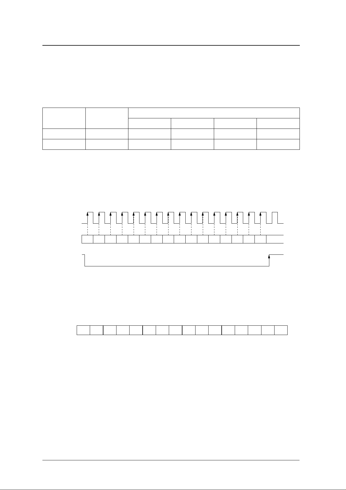
3 wire serial interface is available by using MCK(pin4), MLEN(pin5) and MDT(pin23:FSEL common) pins as
serial mode. At the serial control mode, each enable (fix ed as "LOW" at disable) of output frequency can be set
to stop unnecessary outputs.
MCK
FSEL/MDT
D15 D14 D13 D12 D11 D10 D9 D8 D7 D6 D5 D4 D3 D2 D1 D0
MLEN
Figure 3. Serial control format
16-bit mode resister (MREG) construction in Figure 4. The name and function of each bit are shown in Table 2
and 3. Set the mode-resister D15-D10 as "011100" in the serial control.
0 1 1 1 0 0 RSV CE5 CE4 CE3 CE2 CE1 RSV RSV RSVMREG
D15 D14 D13 D12 D11 D10 D9 D8 D7 D6 D5 D4 D3 D2 D1 D0
RSV
Note: RSV is fixed as LOW .
Figure 4. Mode resister construction
NIPPON PRECISION CIRCUITS—8
Page 9

Table 2. Mode resister function
Bit Name Function
D9 R SV Must be "LOW"
D8 CE5 MO1, MO2 output enable/disable
D7 CE 4 SO5 output enable/disable
D6 CE3 SO3, SO4 output enable/disable
D5 CE 2 SO2 output enable/disable
D4 CE 1 SO1 output enable/disable
D3/D2/D1/D0 R SV Must be "LOW"
Table 3. Clock output control settings(CE5 to 1)
CE5 to CE1 Clock output
LO W Disable (Output fixed as "LOW ")
HIGH Enable (Default)
Note
SM8703AV
Output frequency changes according to the MDT pin condition, as MDT and FSEL pin (Sampling frequency
select signal input) are common. Refer to the section “Settling Time (when the sampling frequenc y is changed)”.
MCK
FSEL/MDT
MLEN
SO2 to 5
MREG (16bit data)
UnstableStable
ts
Stable
Figure 5. Serial transfer timing
NIPPON PRECISION CIRCUITS—9
Page 10

SM8703AV
Settling Time (when the sampling frequency is changed)
The output response when the frequency is changed is shown in figure 6.
FSEL/MDT
SO2
SO3
SO4
SO5
MO1
MO2
SO1
tS
fs = 44.1kHz fs = 44.1kHz
fs = 48kHz
27.0000MHz
33.8688MHz
tS
Figure 6. System clock transient timing
NIPPON PRECISION CIRCUITS—10
Page 11

TYPICAL APPLICATION
SM8703AV
+3.3V
CPU
C3
C4
C1
C2
VDD
VSS
MO1
MCK
MLEN
VDDA
VSSA
XTI
X'tal
XTO
RSV
SM8703AV
MO2
FSEL/MDT
SO5
RSV
SO2
VDD1
VSS1
RSV
SO3
SO4
VDD2RSV
VSS2SO1
+3.3V
27MHz
27MHz
768fs
384fs
C5
512fs
512fs
C6
33.8688MHz
■ Connect the decoupling capacitors (approximately
0.1µF and 1000pF) in parallel, as close to power
supply pins as possible.
■ In order to minimize noise, it is useful to make
VSS as solid pattern.
■ Master clock stability affects the other outputs sta-
bility. In the usage of crystal oscillator, load
capacitor and crystal oscillator should be placed as
close to the SM8703AV as possible, and wired
shortly. Select crystal oscillators and load capacitance carefully, depending on the condition, as
those combination will have influence on the frequency accuracy(C1, C2).
■ Supply pattern including decoupling capacitors
needs careful attention to make the IC’s performance better, since the SM8703AV outputs several high frequency clocks. Pattern capacitance
from output pins should not to be large for prevention of the noise. Connecting output pins to buffers is useful if it is necessary.
■ Power supply and VSS pins.
• VDD : Power supply for digital block
(CPU I/F*, MO1, MO2)
• VSS : VSS for digital block
(CPU I/F*, MO1, MO2)
• VDDA : Power supply for PLL block
(XTI, XTO, PLL/VCO)
• VSSA : VSS for PLL block
(XTI, XTO, PLL/VCO)
• VDD1 : Power supply for output block
(except SO1)
• VSS1 : VSS for output block
(except SO1)
• VDD2 : Power supply for SO1
• VSS2 : VSS for SO1
*: CPU I/F: FSEL/MDT, MLEN, MCK
NIPPON PRECISION CIRCUITS—11
Page 12

SM8703AV
NIPPON PRECISION CIRCUITS INC. reserves the right to make changes to the products described in this data sheet in order to
improve the design or performance and to supply the best possible products. Nippon Precision Circuits Inc. assumes no responsibility for
the use of any circuits shown in this data sheet, conveys no license under any patent or other rights, and makes no claim that the circuits
are free from patent infringement. Applications for any devices shown in this data sheet are for illustration only and Nippon Precision
Circuits Inc. makes no claim or warranty that such applications will be suitable for the use specified without further testing or modification.
The products described in this data sheet are not intended to use for the apparatus which influence human lives due to the failure or
malfunction of the products. Customers are requested to comply with applicable laws and regulations in effect now and hereinafter,
including compliance with export controls on the distribution or dissemination of the products. Customers shall not export, directly or
indirectly, any products without first obtaining required licenses and approvals from appropriate government agencies.
NIPPON PRECISION CIRCUITS INC.
4-3, Fukuzumi 2-chome
Koto-ku, Tokyo 135-8430, Japan
NIPPON PRECISION CIRCUITS INC.
Telephone: 03-3642-6661
Facsimile: 03-3642-6698
NC9902AE 2000.03
NIPPON PRECISION CIRCUITS—12
 Loading...