

Page 1
2 ×
6 ×
2 ×
1 ×
1 ×
SM8702AM
NIPPON PRECISION CIRCUITS INC.
Clock Generator IC
OVERVIEW
The SM8702AM is a clock generator IC that can generate clock signals up to and exceeding 100MHz for personal computer (PC) motherboards. It uses a single 14.318MHz crystal oscillator element and 2 built-in PLLs
to simultaneously and independently generate 2 CPU clocks, 6 PCI bus clocks, 2 reference clocks with the
same frequency as the crystal element, 48MHz USB interface clock, and 24MHz Super I/O chip clock outputs.
It also has 14 outputs that can function as SDRAM clocks by buffering an external input SDRAM clock.
FEATURES
■
Intel
Pentium
compatibles supported
■
2.5/3.3V CPU clock outputs and IOAPIC clock
output
■
14 × SDRAM clock outputs (3 DIMMs)
■
CPU clock outputs
(60), 66, 75, 83, 95, 100, 103, 112, (124), 133MHz
CPU/SDRAM clock frequencies. Values in parentheses are available as mask options.
■
PCI bus clock outputs (one free-running output)
33MHz or 1/2, 1/3, 1/4 of the CPU clock frequency
■
reference clock outputs and 1 × IOAPIC clock
output
14.318MHz REF/IOAPIC clock frequency
■
48MHz USB interface clock output
■
24MHz clock output for Super I/O chip
2
■
I
C serial data bus for frequency/mode output con-
trol
■
CPU-stop and PCI-stop functions
■
Spread Spectrum Clock Generator (SSCG) outputs
Center spread/Down spread, ± 0.5% or ± 1.5%
■
3.3V (VDD) and 2.5/3.3V (VDDL) supply voltages
■
48-pin SSOP package (pin compatible with
ICS9148-26)
II, Pentium
III, and AMD x86-
APPLICATIONS
■
PC motherboards using Intel
tium
II/III, AMD-K6 devices, and x86 architec-
ture CPUs
Pentium
, Pen-
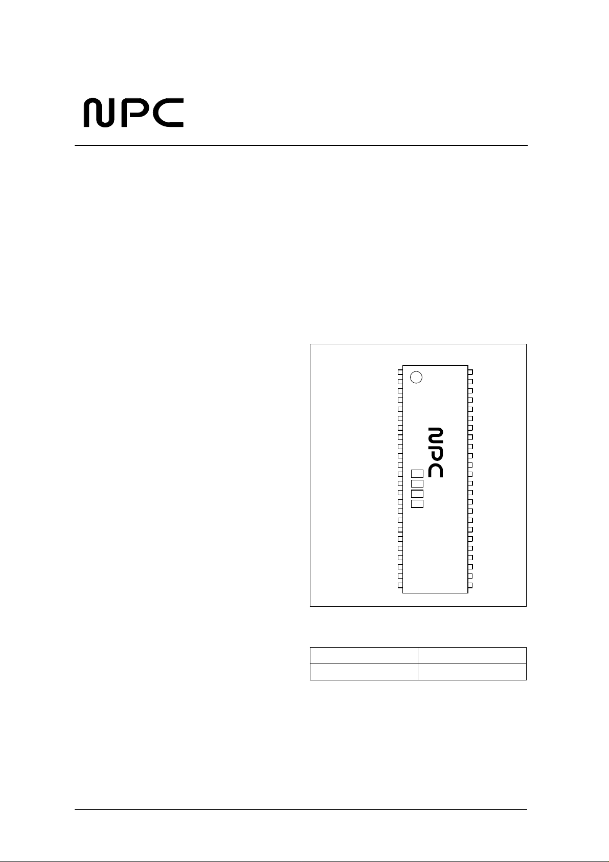
PINOUT
48-pin SSOP (300 mil)
(Top view)
148
VDD1
REF0
VSS
XT
XTN
PCICLK_F/MODE
VDD2
PCICLK0 SDRAM13
VSS
PCICLK1
PCICLK2
PCICLK3
PCICLK4
VDD2
BUFFERIN
VSS
SDRAM11/CPU_STOP#
SDRAM10/PCI_STOP#
VDD3
SDRAM9
SDRAM8
VSS
SDATA
SCLK
24 25
SM8702AM
ORDERING INFORMATION
De vice Pack ag e
SM8702AM 48-pin SSOP
VDDL1
IOAPIC
REF1/FS2
VSS
CPUCLK0
CPUCLK1
VDDL2
SDRAM12
VSS
SDRAM0
SDRAM1
VDD3
SDRAM2
SDRAM3
VSS
SDRAM4
SDRAM5
VDD3
SDRAM6
SDRAM7
VDD4
48MHz/FS0
24MHz/FS1
Intel
and Pentium
are registered trademarks of Intel co..
AMD and AMD-K6 are registered trademarks of Advanced Micro Devices, Inc..
2
I
C Bus is a registered trademark of Philips Electronics N. V..
preliminary
NIPPON PRECISION CIRCUITS—1
Page 2
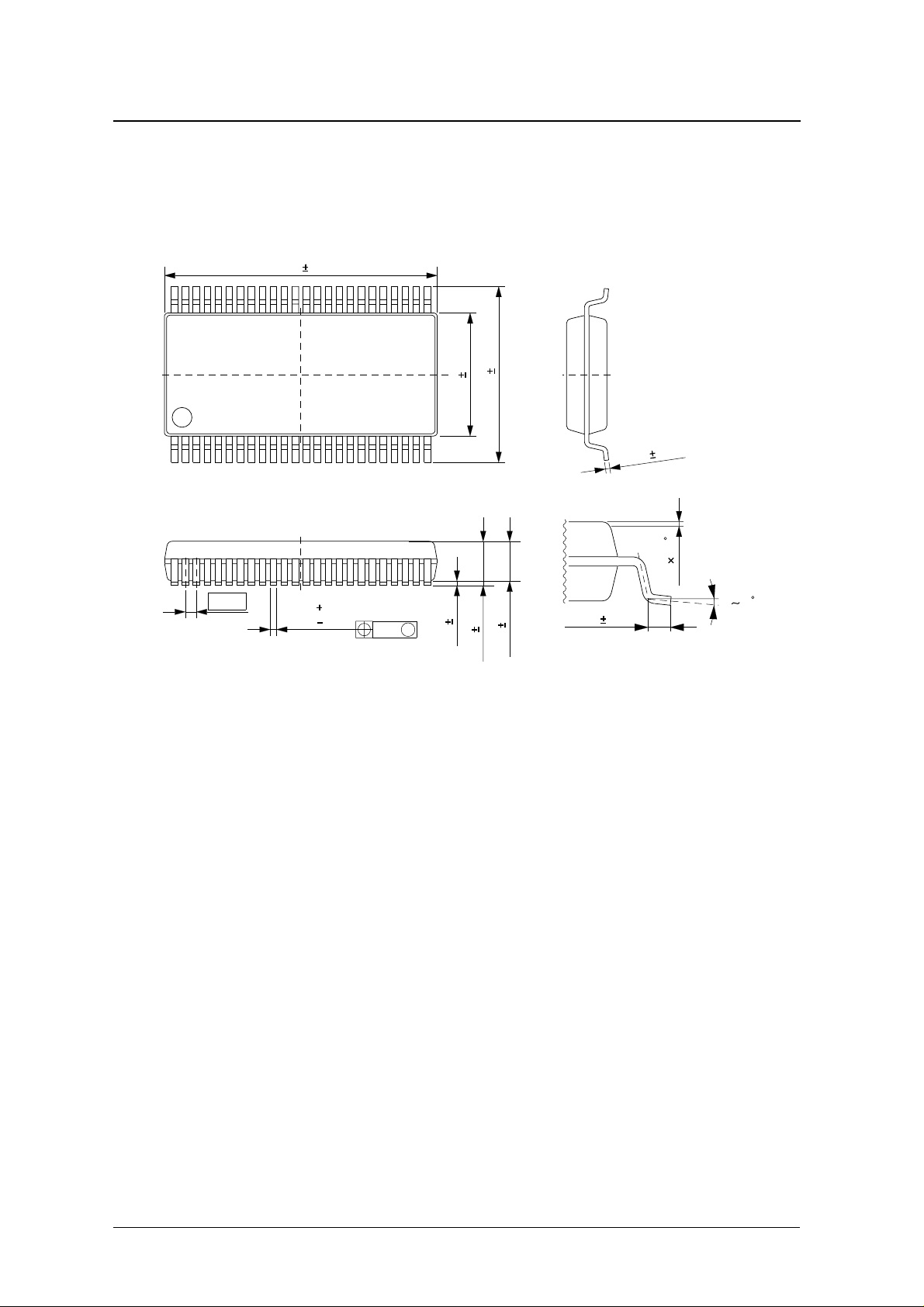
PACKAGE DIMENSIONS
(Unit: mm)
15.85 0.1
SM8702AM
7.50 0.05
10.285 0.125
0.635
0.05
0.25 0.03
0.12
0.20 0.02
0.5 45
0
M
0.3 0.1
2.59 0.15
2.29 0.05
0.80 0.1
8
preliminary
NIPPON PRECISION CIRCUITS—2
Page 3
BLOCK DIAGRAM
SM8702AM
XT XTN
BUFFERIN
FS[0:2]
MODE
Unlock Detector
R-Countor
Buff. Amp.
R-Countor
3
I/O
Latch
Phase
Detector
N-Countor
Phase
Detector
N-Countor
ROM
Unlock Detector
Charge
Pump
Current
Source
SS_CONTROLLER
Charge
Pump
Current
Source
(1st PLL)
VCO
(2nd PLL)
VCO
DIV/3
to DIV/6
DIV/2
DIV/3
1/2
(MS)
5
2
14
2
PCICLK_F
PCICLK
[0:4]
CPUCLK
[0:1]
SDRAM
[0:13]
48MHz
(USB)
24MHz
(Super I/O)
REF[0:1]
IOAPIC
SDATA
SCLK
CPU_STOP#
PCI_STOP#
I C
2
Control Logic
PIN DESCRIPTION
Number Name I/O Function Notes
1 VDD1 – 3.3V supply XT, XTN oscillator, REF[0:1] buffer, stop logic, 3.3V line
2 REF0 I/O 14.318MHz reference clock output
3 VS S – Ground Crystal oscillator, REF[0:1], 3.3Vline
4 X T I Cr ystal oscillator input
5 XT N O C r ystal oscillator output
6 VDD2 – 3.3V supply
PCICLK_F O PCI bus free-running clock output
7
MODE I Mode settings (latch input)
preliminary
8 PCICLK0 O PCI bus clock output
9 V S S – Ground (3.3V supply) PCI clock output buffers, pre-buffer, stop logic
10 PCICLK1 O PCI bus clock output
PCI clock output buffers, pre-buffer, stop logic, and
internal circuit logic supply
CPU_STOP# (pin 17) and PCI_STOP# (pin 18) mode
select pin.
MODE = HIGH: Desktop mode
MODE = LOW: Mobile mode
NIPPON PRECISION CIRCUITS—3
Page 4

SM8702AM
Number Name I/O Function Notes
11 PCICLK2 O PCI bus clock output
12 PCICLK3 O PCI bus clock output
13 PCICLK4 O PCI bus clock output
14 VDD2 – 3.3V supply PCI clock output buffers, pre-buffer, stop logic
15 BUFFERIN I SDRAM clock input
16 VS S – Ground (3.3V supply) SDRAM clock output buffers, pre-buffer, stop logic
SDRAM11
17
18
19 VDD3 – 3.3V supply SDRAM clock output buffers, pre-buffer, stop logic
20 SDRAM9 O SDRAM clock output
21 SDRAM8 O SDRAM clock output
22 VS S – Ground (3.3V supply)
23 SDATA I/O I
24 SCLK I I
25
26
27 VDD4 – 3.3V supply
28 SDRAM7 O SDRAM clock output
29 SDRAM6 O SDRAM clock output
30 VDD3 – 3.3V supply SDRAM clock output buffers, pre-buffer, stop logic
31 SDRAM5 O SDRAM clock output
32 SDRAM4 O SDRAM clock output
33 VS S – Ground (3.3V supply) SDRAM clock output buffers, pre-buffer, stop logic
34 SDRAM3 O SDRAM clock output
35 SDRAM2 O SDRAM clock output
36 VDD3 – 3.3V supply SDRAM clock output buffers, pre-buffer, stop logic
37 SDRAM1 O SDRAM clock output
38 SDRAM0 O SDRAM clock output
39 VS S – Ground (3.3V supply) SDRAM clock output buffers, pre-buffer, stop logic
40 SDRAM12 O SDRAM clock output
41 SDRAM13 O SDRAM clock output
42 VDDL2 – 2.5/3.3V supply CPU clock output buffers, pre-buffer, stop logic
43 CPUCLK1 O CPU clock output
44 CPUCLK0 O CPU clock output
45 V S S – Ground (2.5/3.3V supply) CPU clock output buffers, pre-buffer, stop logic
46
47 IOAPIC O 14.318MHz IOAPIC clock output
48 VDDL1 – 2.5/3.3V supply IOAPIC output buffer, pre-buffer, stop logic
CPU_STOP# CPU clock outputs stop control
SDRAM10
PCI_STOP# PCI clock outputs stop control
24MHz
FS 1 Frequency select 1 (latch input)
48MHz
FS 0 Frequency select 0 (latch input)
preliminary
REF1
FS 2 Frequency select 2 (latch input)
SDRAM clock output
I/O
SDRAM clock output
I/O
2
C s er ial data input
2
C clock input
24MHz clock output
I/O
48MHz USB clock output
I/O
14.318MHz reference clock output
I/O
Input on BUFFERIN is buffered and then output on
SDRAM[0:13]
In mobile mode (MODE = LOW), CPUCLK[0:1] tied LOW
when CPU_STOP# = LOW.
In mobile mode (MODE = LOW), PCICLK[0:4] tied LOW
when PCI_STOP# = LOW.
PLL and internal logic ground, I
24MHz/48MHz output ground
2
I
C interface , 24MHz/48MHz output supply, PLL and
internal logic supply
2
C interface ,
NIPPON PRECISION CIRCUITS—4
Page 5
) −
) −
SPECIFICATIONS
Absolute Maximum Ratings
VDD:VDD1, VDD2, VDD3, VDD4
VDDL:VDDL1, VDDL2 unless otherwise noted.
Parameter Symbol Rating Unit
DD1
, V
(V
DD2
V
DDL1
V
DDL
V
OUT
(V
Supply voltage range
Input voltage range V
Output voltage range V
Storage temperature range T
Po w er dissipation P
SM8702AM
DD
, V
, V
DD3
DD4
, V
DDL2
SS
IN
stg
D
−
−
−
°
°
0.3 to 6.0 V
0.3 to 6.0 V
0V
0.3 to V
0.3 to V
+ 0.3 V
DD
+ 0.3 V
DD
55 to 125
0.8 W
C
Recommended Operating Conditions
V
= 0V
SS
Parameter Symbol Condition
(V
DD1
V
(V
DD3
DDL1
Supply voltages
Operating temperature range T
Maximum load capacitance
Reference frequency f
V
V
C
C
C
DD
, V
, V
DDL
, V
opr
L1
L2
L3
REF
Excludes internal core, CPU
,
clock and IOAPIC output
DD2
)
stages
DD4
Internal core, CPU clock
)
and IOAPIC output stages
DDL2
CPUCLK 10 – 20 pF
PCICLK, SDRAM 20 – 30 pF
RE F, 24/48MHz, IOAPIC 10 – 20 pF
Rating
Unit
min typ max
3.135 3.300 3.465 V
2.375 2.500 2.625 V
0–70
– 14.318 – MH z
C
preliminary
NIPPON PRECISION CIRCUITS—5
Page 6

DC Electrical Characteristics
T
= 0 to 70 ° C, V
a
= 3.3V ± 5%, V
DD
= 2.5V ± 5%, V
DDL
SM8702AM
= 0V unless otherwise noted.
SS
−
−
−
−
Parameter Symbol Condition
HIGH-level input voltage V
All pins excl. X T, XT N 2.0 – V
IH
All pins excl. X T, XTN, SDATA, SCLK V
L O W -level input voltage V
HIGH-level input current I
L O W -level input current I
HIGH-level output voltage V
L O W-level output voltage V
HIGH-level output voltage V
L O W-level output voltage V
IL
SD ATA, SCLK: I
V
IH
IH
V
IL
IL
All clock outputs:
OH(3.3V)
I
OH
All clock outputs:
OL(3.3V)
I
OL
CPUCLK[0:1], IOAPIC:
OH(2.5V)
I
OH
CPUCLK[0:1], IOAPIC:
OL(2.5V)
I
OL
= V
DD
= 0V – – 1 0 µA
=
1mA, V
= 1mA, V
DD
=
1mA, V
= 1mA, V
DDL
CPUCLK[0:1]: V
PCICLK_F, PCICLK[0:4]:
V
= 2.0V
OH
HIGH-level output current I
OH
SDRAM[0:13]: V
REF[0:1], 24/48MHz:
V
= 2.0V
OH
IOAPIC: V
= 1.7V 8.5 – 23.0
OH
CPUCLK[0:1]: V
PCICLK_F, PCICLK[0:4]:
V
= 0.8V
OL
L O W-level output current I
OL
SDRAM[0:13]: V
REF[0:1], 24/48MHz:
V
= 0.8V
OL
= 0.7V 11.0 – 25.3
OL
= 0pF, V
= 0pF, V
= 0pF, V
= 3.465V
DD
DDL
DDL
Output leakage current I
Current consumption
IOAPIC: V
Outputs high impedance
OZ
I
C
DD
L
C
DDL1
I
DDL2
L
C
L
Rating
min typ max
– 0.8
– 0.7
2
C interface V
SS
SS
10 – 10 µA
= 3.135V
DD
= 3.135V
= 2.375V
DDL
= 2.375V
= 1.7V
OH
PCICLK, SDRAM, REF,
24/48MHz pins.
Also, CPUCLK[0:1] and
IOAPIC outputs, when
VDDL[1:2] = 3.3V.
CPUCLK[0:1] and
IOAPIC outputs, when
VDDL[1:2] = 2.5V.
2.4 – – V
– – 0.4 V
2.0 – – V
– – 0.4 V
8.5 23.0
18.7 – 42.6
f
= 2.0V 18.7 – 42.6
OH
= 66.5MHz
OUT
18.7 – 42.6
= 0.7V
OL
11.0 – 25.3
18.7 – 40.3
= 0.8V 18.7 – 40.3
OL
= 66.5MHz
f
OUT
18.7 – 40.3
10 – 10 µA
– – 180
f
= 3.465V – – 30
= 66.5MHz
OUT
= 2.625V – – 20
DD
Unit
V
V
mA
mA
mAI
preliminary
NIPPON PRECISION CIRCUITS—6
Page 7

AC Electrical Characteristics
CPU clock characteristics 1
T
= 0 to 70 ° C, V
a
wise noted.
= 3.3V ± 5%, V
DD
= 2.5V ± 5%, V
DDL
SM8702AM
= 0V, f
SS
= 14.318MHz, CL = 20pF unless other-
X’tal
Parameter Symbol Condition
Output clock rise time
Output clock fall time
Duty cycle Dt VT = 1.25V 45 50 55 %
Output clock jitter
Output clock skew
Clock frequency stabilize time
Output impedance
1. Design maximum values, not 100% guaranteed.
2. Design estimate values, not 100% guaranteed.
1
1
1
1
2
1
t
VOL = 0.4V → VOH = 2.0V transition time – – 2.0 n s
r
t
VOH = 2.0V → VOL = 0.4V transition time – – 2.0 n s
f
t
VT = 1.25V, rising edge Cycle-to-cycle jitter – – 2 5 0 ps
jc
t
skwVT
t
stb
Z
O
= 1.25V, rising edge
Cold start
VO = 0.5V
DDL
Between CPUCLK0 and
CPUCLK1
Supply ON (VDD = 3.3V)
until clock reaches
specified frequency
min typ max
10–90Ω
Rating
– – 250 ps
––3ms
CPU clock characteristics 2
Ta = 0 to 70°C, VDD = V
Parameter Symbol Condition
Output clock rise time
Output clock fall time
Duty cycle Dt VT = 1.5V 45 50 55 %
Output clock jitter
Output clock skew
Clock frequency stabilize time
Output impedance
1. Design maximum values, not 100% guaranteed.
2. Design estimate values, not 100% guaranteed.
1
1
1
1
2
= 3.3V ± 5%, VSS = 0V, f
DDL
t
VOL = 0.4V → VOH = 2.4V transition time – – 2.5 n s
r
t
VOH = 2.4V → VOL = 0.4V transition time – – 2.5 n s
f
t
VT = 1.5V, rising edge Cycle-to-cycle jitter – – 2 5 0 ps
jc
1
t
skwVT
t
stb
Z
O
Cold start
VO = 0.5V
= 1.5V, rising edge
DDL
= 14.318MHz, CL = 20pF unless otherwise noted.
X’tal
Rating
min typ max
Between CPUCLK0 and
CPUCLK1
Supply ON (VDD = 3.3V)
until clock reaches
specified frequency
– – 250 ps
––3ms
10–60Ω
Unit
Unit
preliminary
NIPPON PRECISION CIRCUITS—7
Page 8

PCI clock characteristics
SM8702AM
Ta = 0 to 70°C, VDD = 3.3V ± 5%, VSS = 0V, f
Parameter Symbol Condition
Output clock rise time
Output clock fall time
Duty cycle Dt VT = 1.5V 45 50 55 %
Output clock jitter
Output clock skew
CPU/PCI clock skew
Clock frequency stabilize time
Output impedance
1. Design maximum values, not 100% guaranteed.
2. CPUCLK and PCICLK rising edges, V
3. Design estimate values, not 100% guaranteed.
1
1
1
1
2
3
1
t
VOL = 0.8V → VOH = 2.4V transition time – – 2.0 n s
r
t
VOH = 2.4V → VOL = 0.8V transition time – – 2.0 n s
f
t
VT = 1.5V, rising edge Cycle-to-cycle jitter – – 25 0 ps
jc
t
skwVT
t
hpsk
t
stb
Z
O
T-CPUCLK
V
V
edges
Cold start
VO = 0.5V
= 1.5V, rising edge
= 1.25/1.5V,
T-CPUCLK
= 1.5V, rising
T-PCICLK
DD
= 1.25V (V
= 14.318MHz, CL = 30pF unless otherwise noted.
X’tal
Rating
min typ max
Between PCI clocks:
PCICLK_F and
PCICLK[0:4]
Between CPU and PCI
clocks: CPUCLK[0:1] and
PCICLK_F/PCICLK[0:4]
Supply ON (VDD = 3.3V)
until clock reaches
specified frequency
= 2.5V)/1.5V (V
DDL
= 3.3V), V
DDL
T-PCICLK
– – 250 ps
1.0 2.2 4.0 ns
––3ms
10–60Ω
= 1.5V skew measurement.
SDRAM clock characteristics
Unit
Ta = 0 to 70°C, VDD = V
Parameter Symbol Condition
Output clock rise time
Output clock fall time
Duty cycle
Output clock skew
Input to output propagation
delay
Output impedance
1. Design maximum values, not 100% guaranteed.
2. BUFFERIN and SDRAM rising edges, V
3. Design estimate values, not 100% guaranteed.
1
2,3
1
1
1
3
= 3.3V ± 5%, VSS = 0V, f
DDL
t
VOL = 0.8V → VOH = 2.4V transition time – – 2.0 n s
r
t
VOH = 2.4V → VOL = 0.8V transition time – – 2.0 n s
f
V
= 1.5V, BUFFERIN
T
Dt
input clock signal rise
and fall time rate ≥ 1V/ns
VT = 1.5V, rising edge,
BUFFERIN input clock
t
skw
signal rise and fall time
rate ≥ 1V/ns
V
T-BUFFERIN
V
T-SDRAM
t
edges, BUFFERIN input
pd
clock signal rise and fall
time rate ≥ 1V/ns
Z
VO = 0.5V
O
T-BUFFERIN
preliminary
= 14.318MHz, CL = 30pF unless otherwise noted.
X’tal
3.3V BUFFERIN input
clock signal logic level
Between SDRAM clocks:
SDRAM[0:13]
= 1.5V,
= 1.5V, rising
DD
= 1.5V (logic level = 3.3V), V
Between BUFFERIN and
SDRAM[0:13]
= 1.5V delay measurement.
T-SDRAM
Rating
Unit
min typ max
40 50 60 %
– 200 600 ps
– 5.5 7.0 ns
10–60Ω
NIPPON PRECISION CIRCUITS—8
Page 9

SM8702AM
24MHz/48MHz, REF[0:1] clock characteristics
Ta = 0 to 70°C, VDD = 3.3V ± 5%, VSS = 0V, f
Parameter Symbol Condition
Output clock rise time
Output clock fall time
Duty cycle
Output clock jitter
Clock frequency stabilize time
Output impedance
1. Design maximum values, not 100% guaranteed.
2. Design estimate values, not 100% guaranteed.
1
1
1
1
2
t
VOL = 0.8V → VOH = 2.4V transition time – – 2.0 n s
r
t
VOH = 2.4V → VOL = 0.8V transition time – – 2.0 n s
f
Dt VT = 1.5V 40 50 60 %
t
VT = 1.5V, rising edge Absolute jitter – 2 5 0 8 0 0 ps
jc
1
t
Cold start
stb
Z
VO = 0.5V
O
DD
IOAPIC clock characteristics
Ta = 0 to 70°C, VDD = 3.3V ± 5%, VSS = 0V, f
Parameter Symbol Condition
VOL = 0.8V → VOH = 2.4V transition time,
V
= 3.3V
Output clock rise time
Output clock fall time
Duty cycle
Output clock jitter
Clock frequency stabilize time
Output impedance
1. Design maximum values, not 100% guaranteed.
2. Design estimate values, not 100% guaranteed.
1
1
1
1
1
2
Z
DDL1
t
r
VOL = 0.4V → VOH = 2.0V transition time,
V
= 2.5V
DDL1
VOH = 2.4V → VOL = 0.8V transition time,
V
= 3.3V
DDL1
t
f
VOH = 2.0V → VOL = 0.4V transition time,
V
= 2.5V
DDL1
Dt VT = 1.5V, V
t
VT = 1.5V, rising edge Absolute jitter – 2 5 0 8 0 0 ps
jc
t
Cold start
stb
VO = 0.5V
O
DDL1
DD
= 14.318MHz, CL = 20pF unless otherwise noted.
X’tal
Rating
min typ max
Supply ON (VDD = 3.3V)
until clock reaches
specified frequency
= 14.318MHz, CL = 20pF unless otherwise noted.
X’tal
= 3.3V 40 50 60 %
Supply ON (VDD = 3.3V)
until clock reaches
specified frequency
––3ms
10–60Ω
Rating
min typ max
– – 2.0
– – 2.0
– – 2.0
– – 2.0
––3ms
10–90Ω
Unit
Unit
ns
ns
preliminary
NIPPON PRECISION CIRCUITS—9
Page 10

SM8702AM
I2C serial interface electrical characteristics
Ta = 0 to 70°C, VDD = 3.3V ± 5%, VSS = 0V, f
Parameter Symbol Condition
Se r ial clock frequency f
Se r ial clock star t state hold time t
Se r ial clock LOW-level pulsewidth t
Se r ial clock HIGH-level pulsewidth t
Successive star t state setup time t
Data hold time t
Data input setup time t
Pulse rise time t
Pulse fall time t
Stop state setup time t
Se r ial data bus buffer time t
Bus line load capacitance C
HD;STA
SU;STA
HD;DAT
SU;DAT
SU;STO
I2C standard mode 0 – 1 00 k Hz
SCLK
LOW
HIGH
I2C device data 0 – 3.45 µs
r
f
BUF
b
= 14.318MHz, CL = 30pF unless otherwise noted.
X’tal
Rating
min typ max
4.0 – – µ s
4.7 – – µ s
4.0 – – µ s
4.7 – – µ s
250 – – ns
– – 1000 ns
– – 300 ns
4.0 – – µ s
4.7 – – µ s
– – 400 pF
Unit
tBUF
SDATA
SCLK
tr
tSU;STO
tHD;STA
tf
tLOW
tHD;DAT
tr
tSU;DAT
tHD;STA
tf
tSU;STA
tHIGH
I2C ser ial data timing
preliminary
NIPPON PRECISION CIRCUITS—10
Page 11

SM8702AM
FUNCTIONAL DESCRIPTION
Mode Setting Overview
There are 2 methods that can be used to set the frequency and clock output start/stop operating modes.
■ Using external inputs (pins 7, 17, 18, 25, 26, 46) or,
■ Using data read in from an I
The default state is where the operating state is set by external pin control. Thus, the output frequency can be
set by FS[0:2] (pins 25, 26, 46). Note that the SSCG function is OFF in this case. If the I2C serial data byte 0
bit 3 is set to 1, then the output frequency is determined by data using the I2C interface. Then, the Spread Spectrum function (SSCG) can be selected using I2C data. However, if mode settings using I2C data and external
pin control conflict or overlap, the mode settings dictated by I2C data have precedence over external pin control.
During normal operation, pins 17 and 18 can function as SDRAM clock outputs (desktop mode) or they can
function as CPUCLK output stop control and PCICLK output stop control (mobile mode), depending on the
state of MODE (pin 7) when power is first applied.
In addition to output frequency settings, other operating mode settings which can be controlled by I2C serial
data include SSCG operation and mode, and output pin grouping enable/disable switching.
Hardware Frequency Selection
When power is applied, the frequency setting is controlled by FS[0:2] when byte 0 bit 3 is set to 0. Note that if
byte 0 bit 3 is set to 1, the frequency is selected by bits 4 to 6 in the same manner as inputs FS0 to FS2.
Inputs Output frequency
FS2 FS1 FS0
HIGH HIGH HIGH 100.2 33.4
HIGH HIGH LOW 133 33.2
HIGH LOW HIGH 112.1 37.3
HIGH LOW LOW 103 34.3
LOW HIGH HIGH 66.5 33.2
LOW HIGH LOW 83.3 41.6
LOW L OW HIGH 74.9 37.4
LO W L OW L O W 94.7 31.6
2
C serial interface.
CPUCLK
[MHz]
PCICLK
[MHz]
Mode and Power Management Inputs
The SM8702AM supports 2 operating modes, desktop mode and mobile mode, selected by MODE (pin 7).
If MODE is HIGH when power is first applied, desktop mode is selected. In this mode, pins 17 and 18 function
as SDRAM clock outputs, SDRAM11 and SDRAM10, respectively.
If MODE is LOW when power is first applied, mobile mode is selected. In this mode, pins 17 and 18 function
as the CPU clock (CPUCLK[0:1]) and PCI clock (PCICLK[0:4]) output stop control signal inputs,
CPU_STOP# and PCI_STOP#, respectively. This function is used mainly to reduce power consumption.
MODE Pin 17 Pin 18 Mode
HIGH SDRAM11 SDRAM10
LOW CPU_STOP# PCI_STOP#
preliminary
Desktop mode
Pins 17 and 18 are outputs.
Mobile mode
Pins 17 and 18 are inputs.
NIPPON PRECISION CIRCUITS—11
Page 12

SM8702AM
Operating Mode Summary
The state of the various external inputs and outputs in the operating modes is indicated in the following table.
MODE
MODE = HIGH
(desktop
mode)
MODE = LOW
(mobile mode)
1. Enabled = output functions active . Disabled = LOW-level output.
SDRAM11/
CPU_STOP#
Enabled
(SDRAM output)
HIGH
(CPU_STOP# input)
HIGH
(CPU_STOP# input)
LOW
(CPU_STOP# input)
LOW
(CPU_STOP# input)
SDRAM10/
PCI_STOP#
Enabled
(SDRAM output)
HIGH
(PCI_STOP# input)
LOW
(PCI_STOP# input)
HIGH
(PCI_STOP# input)
LOW
(PCI_STOP# input)
CPUCLK[0:1] PCICLK[0:4]
Enabled Enabled Enabled Enabled Enabled
Enabled Enabled Enabled Enabled Enabled
Enabled Disabled Enabled Enabled Enabled
Disabled Enabled Enabled Enabled Enabled
Disabled Disabled Enabled Enabled Enabled
PCICLK_F,
24MHz/48MHz,
SDRAM[0:13]
Cr ystal
oscillator
VCO
(internal
signal)
1
Notes
Desktop mode.
Pins 17 and 18
function as outputs.
Mobile mode.
Pins 17 and 18
function as inputs.
Pin 17 =
CPU_STOP#
Pin 18 =
PCI_STOP#
CPU Clock Stop Function
In mobile mode, selected using MODE (pin 7), the CPUCLK[0:1] clock outputs can be stopped by external pin
control. The asynchronous stop signal input on CPU_STOP# is sampled internally on the rising edge of the
PCI free-running output clock (PCICLK_F).
When CPU_STOP# goes LOW, the CPU clock outputs (CPUCLK) stop after a delay of 2 to 4 clock cycles.
When CPU_STOP# goes HIGH, the CPU clock outputs start after a delay of 2 to 4 clock cycles. The actual
start and stop delay varies with the output frequency up to a maximum of 4 CPU clock cycles.
CPUCLK
(internal)
PCICLK
(internal)
PCICLK_F
(free-running)
CPU_STOP#
PCI_STOP#
(All "H")
CPUCLK
(external)
preliminary
NIPPON PRECISION CIRCUITS—12
Page 13

SM8702AM
PCI Clock Stop Function
In mobile mode, selected using MODE (pin 7), the PCICLK[0:4] clock outputs can be stopped by external pin
control, in the same way as the CPU clock stop function.
When PCI_STOP# goes LOW, the PCI clock outputs (PCICLK) stop, and when PCI_STOP# goes HIGH, the
PCI clock outputs start. In either case, the PCI_STOP# signal is sampled internally on the rising edge of PCICLK, and the output state transition occurs with 1 PCI clock cycle delay.
CPUCLK
(internal)
PCICLK
(internal)
PCICLK_F
(free-running)
CPU_STOP#
(All "H")
PCI_STOP#
PCICLK
(external)
preliminary
NIPPON PRECISION CIRCUITS—13
Page 14

SM8702AM
I2C Bus Serial Data Format
The format of the I2C serial data on SDATA (pin 23) which is input in sync with the serial data clock on SCLK
(pin 24) is shown below.
The SM8702AM I2C address is given below.
A6 A5 A4 A3 A2 A1 A0 R/W#
1101001−
R/W# = 0 or 1
In the start sequence, the I2C bus serial data is fed into the clock generator in the following direction.
1. I2C address with R/W# = 0
2. ACK acknowledge bit
3. Two successive 8-bit dummy command code data words (including ACK acknowledge bit)
4. 8-bit dummy command code (Byte 0 to Byte 5)
The direction of I C Data for Clock Generator
2
I C Addr.
+R/W#
The data transfer speed is 100k bps (I2C standard mode), with input logic level of 3.3V. When power is first
applied, all internal registers are restored to their default state as below.
■ Byte0 : default = 0 (bit 0 to bit 3 and bit 7)
■ Byte 1 to Byte 5 : default = 1 (all bits)
A
C
K
D2h
: default = 1 (bit 4 to bit 6)
2
A
Dummy
C
Command
K
8bit1bit 8bit1bit
Code
8bit1bit
Dummy
Command
Code
Bit 7 Bit 6 Bit 5 Bit 4 Bit 3 Bit 2 Bit 1 Bit 0
8bit 1bit
A
Byte 0 Byte 1 Byte 2
C
K
8bit 1bit
A
C
K
8bit 1bit
A
C
K
1bit
S
A
C
K
Byte 5
A
T
C
O
K
P
preliminary
NIPPON PRECISION CIRCUITS—14
Page 15

I2C Bus Data Bytes
Byte 0: function and frequency select
SM8702AM
Bit Function
7
6:4
3
2
1
0
0: Spread spectru m ± 1.5% modulation
1: Spread spectru m ± 0.5% modulation
Frequency select bits
Bit 6 Bit 5 Bit 4
1 1 1 100.2 33.4
1 1 0 133 33.2
1 0 1 112.1 37.3
1 0 0 103 34.3
0 1 1 66.5 33.2
0 1 0 83.3 41.6
0 0 1 74.9 37.4
0 0 0 94.7 31.6
0: Hardware frequency select using FS[0:2]
2
C b us serial data frequency select
1: I
0: Spread spectrum center spread select
1: Spread spectru m down spread select
0: Normal operating mode (SSCG disabled)
1: Spread spectru m operating mode (SSCG enabled)
0: Nor mal output mode (running)
1: Three-state output mode
CPUCLK
[MHz]
PCICLK
[MHz]
Power-ON
default
0
1
0 FS[0:2] are latch inputs
0
0
0 All outputs are high impedance when bit 0 is set to 1.
The spread spectrum accuracy of modulation is not
guaranteed.
The power-ON default for bits 4 to 6 is 1.
When bit 3 is set to 1 (I
the frequency in the same write cycle timing.
Notes
2
C select), bits 4 to 6 select
Byte 1: CPU register Byte 2: PCI register
Pin
Bit
number
7 26 1 48MHz USB
6 25 1 24MHz (Super I/O)
5 – 1 (Reser ved)
4 – 1 (Reser ved)
3 – 1 (Reser ved)
2 – 1 (Reser ved)
1 43 1 CPUCLK1 enable
0 44 1 CPUCLK0 enable
1. 1 = enabled, 0 = disabled
Power-ON
1
default
Notes
Bit
7 – 1 (Reser ved)
6 7 1 PCICLK_F enable
5 – 1 (Reser ved)
4 14 1 PCICLK4 enable
3 12 1 PCICLK3 enable
2 11 1 PCICLK2 enable
1 10 1 PCICLK1 enable
0 8 1 PCICLK0 enable
1. 1 = enabled, 0 = disabled
Pin
number
Power-ON
default
preliminary
1
Notes
NIPPON PRECISION CIRCUITS—15
Page 16

SM8702AM
Byte 3: SDRAM register
Pin
41
32
38
Power-ON
1
default
1 SDRAM[8,9,12,13] enable
1 SDRAM[4:7] enable
1 SDRAM[0:3] enable
Bit
number
7 – 1 (Reser ved)
6 – 1 (Reser ved)
5 – 1 (Reser ved)
4 – 1 (Reser ved)
3 17, 18 1
20, 21, 40,
2
28, 29, 31,
1
34, 35, 37,
0
1. 1 = enabled, 0 = disabled
Byte 4: Reserved register
Pin
Bit
number
7 – 1 (Reser ved)
6 – 1 (Reser ved)
5 – 1 (Reser ved)
4 – 1 (Reser ved)
3 – 1 (Reser ved)
2 – 1 (Reser ved)
1 – 1 (Reser ved)
0 – 1 (Reser ved)
1. 1 = enabled, 0 = disabled
Power-ON
1
default
Notes
SDRAM[10:11] enable in
desktop mode only (MODE =
HIGH)
Notes
Byte 5: REF/IOAPIC register
Pin
Bit
number
7 – 1 (Reser ved)
6 – 1 (Reser ved)
5 – 1 (Reser ved)
4 47 1 IOAPIC enable
3 – 1 (Reser ved)
2 – 1 (Reser ved)
1 46 1 REF1 enable
0 2 1 REF0 enable
1. 1 = enabled, 0 = disabled
Power-ON
1
default
Notes
preliminary
NIPPON PRECISION CIRCUITS INC. reserves the right to make changes to the products described in this data sheet in order to
improve the design or performance and to supply the best possible products. Nippon Precision Circuits Inc. assumes no responsibility for
the use of any circuits shown in this data sheet, conveys no license under any patent or other rights, and makes no claim that the circuits
are free from patent infringement. Applications for any devices shown in this data sheet are for illustration only and Nippon Precision
Circuits Inc. makes no claim or warranty that such applications will be suitable for the use specified without further testing or modification.
The products described in this data sheet are not intended to use for the apparatus which influence human lives due to the failure or
malfunction of the products. Customers are requested to comply with applicable laws and regulations in effect now and hereinafter,
including compliance with export controls on the distribution or dissemination of the products. Customers shall not export, directly or
indirectly, any products without first obtaining required licenses and approvals from appropriate government agencies.
NIPPON PRECISION CIRCUITS INC.
4-3, Fukuzumi 2-chome
Koto-ku, To kyo 135-8430, Japan
NIPPON PRECISION CIRCUITS INC.
Telephone: 03-3642-6661
Facsimile: 03-3642-6698
NP9907AE 1999.07
NIPPON PRECISION CIRCUITS—16
 Loading...