

Page 1
−
SM8580AM
Real-time Clock IC with 4-bit Interface
NIPPON PRECISION CIRCUITS INC.
OVERVIEW
The SM8580AM is a real-time clock IC based on a 32.768 kHz crystal oscillator, which features a 4-bit parallel interface for communication with an external microcontroller.
It comprises second-counter to year-counter clock and calendar circuits that feature automatic leap-year adjustment up to year 2099, alarm and timer interrupt functions, clock counter change detect functions, ±30-second
correction function, time error correction function, and built-in temperature sensor.
The 4-bit parallel interface is compatible with general-purpose SRAM over a high-speed bus.
and Built-in Temperature Sensor
FEATURES
■
High-speed bus 4-bit parallel interface
■
Date, day, hour, minute, and second-counter presettable alarm interrupt
■
1/4096 seconds to 255 minutes presettable interval
timer interrupt function
■
2 software-maskable alarm and timer interrupt
outputs
■
Clock counter change detect functions
■
4-digit western calendar display
■
Automatic leap year correction up to year 2099
■
±30-second adjust function
■
195 to +192ppm time error correction range
■
Built-in temperature sensor (analog voltage output)
■
2.4 to 5.5V interface voltage range
■
1.6 to 5.5V clock voltage range
■
0.6µA/3V (typ) current consumption
ORDERING INFORMATION
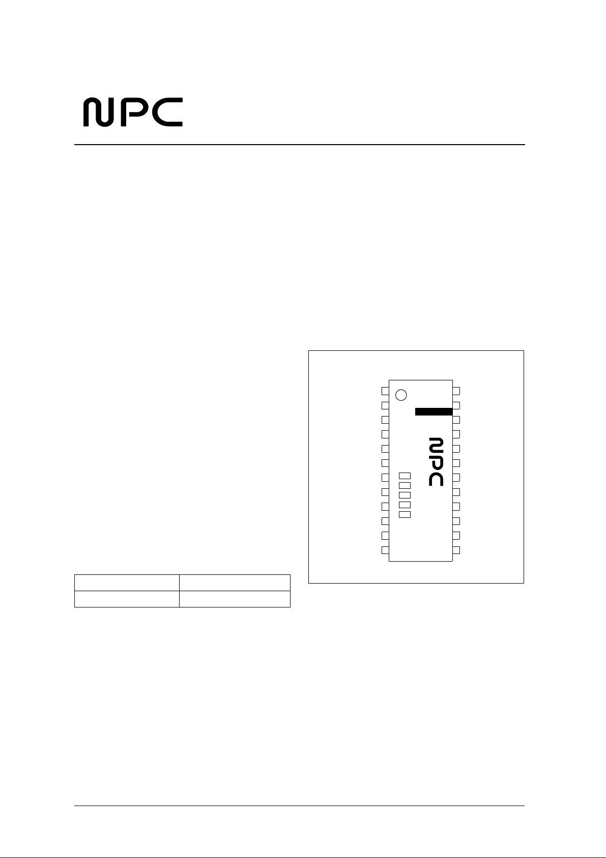
De vice Pack ag e
SM8580AM 24-pin SSOP
PINOUT
(Top view)
CE0N
FCON
FOUT
VTEMP
AIRQN
TIRQN
A0
A1
A2
A3
RDN
VSS
1
SM8580AM
12
24
VDD
XT
XTN
N.C.
N.C.
N.C.
CE1
D0
D1
D2
D3
13
WRN
NIPPON PRECISION CIRCUITS—1
Page 2
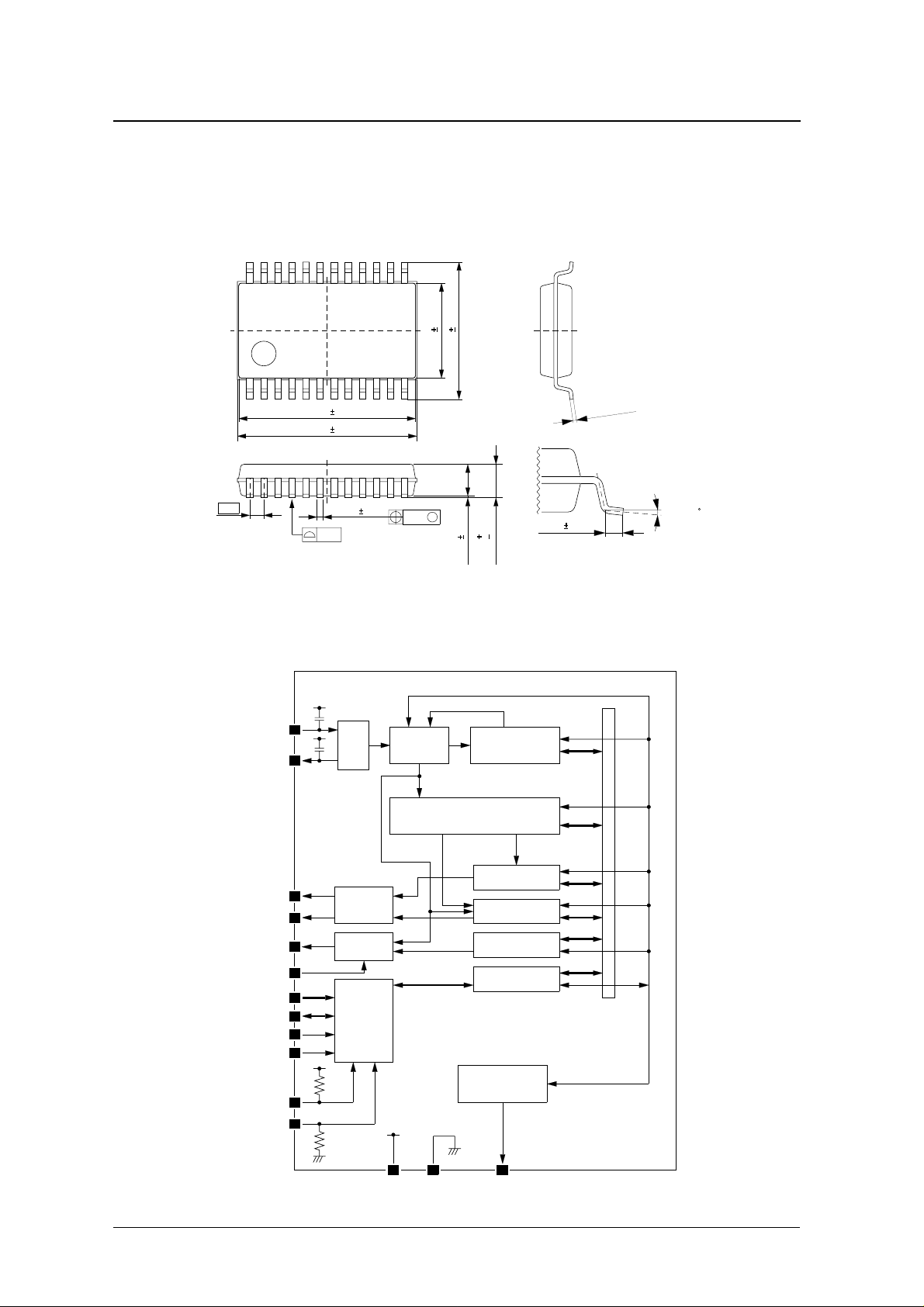
PACKAGE DIMENSIONS
(Unit: mm)
24-pin SSOP
10.05 0.20
10.20 0.30
SM8580AM
7.80 0.30
5.40 0.20
0.15
+
−
0.1
0.05
0.8
BLOCK DIAGRAM
XTN
AIRQN
TIRQN
FOUT
FCON
A0 to A3
D0 to D3
WRN
RDN
CE0N
XT
CE1
0.36 0.10
0.10
CG
CD
OSC
Interrupt
Control
FOUT
Control
BUS
Interface
M
0.12
Divider
Clock and Calendar
1.80
0.10
0.20
1.90
0.10 0.10
Digital Trimming
Controller
Counter
Alarm Register
Timer Register
FOUT Register
Control Register
Temperature
Sensor
0.50 0.20
Control line
0 to 10
VDD VSS
VTEMP
NIPPON PRECISION CIRCUITS—2
Page 3

PIN DESCRIPTION
SM8580AM
Number Name I/O Function
1 CE0N I
2 FCON I
3 FOUT O Frequency set register, frequency output (CMOS output)
4 VTEMP O Temperature voltage output (analog output)
5 AIRQN O Alarm interrupt output (N-channel open-drain output)
6 TIRQN O Timer interrupt output (N-channel open-drain output)
7A0I
8A1I
9A2I
10 A3 I
11 RDN I
12 VS S – Ground
13 WRN I
14 D 3 I/O
15 D 2 I/O
16 D 1 I/O
17 D 0 I/O
18 CE1 I
19 NC – No connection
20 NC – No connection
21 NC – No connection
22 X T N O Oscillator output, with built-in oscillator capacitance C
23 XT I Oscillator output, with built-in oscillator capacitance C
24 V D D – Supply
1. Connect a 0.1µF capacitor between VDD and VS S.
Chip enable 0 input with built-in pull-up resistor.
The SM8580AM can be accessed when CE0N is LOW and CE1 is HIGH.
FOUT output frequency select control input (when CE1 is HIGH).
32.768kHz fixed frequency output when FCON is LOW.
Output frequency determined by bit FD when FCON is HIGH (when FE bit is 1).
Note that a HIGH-level voltage should be applied to FCON to avoid unwanted 32.768kHz output during
backup.
Address inputs.
Connect to the microcontroller address bus.
The selected register address is input on this bus when accessing the SM8580AM (positive logic).
Read strobe input. Data can be read from SM8580AM when RDN is LOW and WRN is HIGH.
An error will occur if both RDN and WRN are simultaneously LOW.
W rite strobe input. Data can be written to SM8580AM when RDN is HIGH and WRN is LOW.
An error will occur if both RDN and WRN are simultaneously LOW.
Data bus input/outputs.
Connect to the microcontroller data bus.
Chip enable 1 input with built-in pull-down resistor.
The SM8580AM can be accessed when CE0N is LOW and CE1 is HIGH.
FOUT is in output mode when CE1 is HIGH, regardless of the state of CE0N. FOUT is high impedance
when CE1 is LOW.
1
D
G
NIPPON PRECISION CIRCUITS—3
Page 4
−
−
−
−
−
° C
−
°
SM8580AM
FOUT Output and SM8580AM Access Relationship
CE0N CE1 FCON FE bit FOUT output SM8580AM accessible
HIGH L OW
LOW LOW
HIGH HIGH
LOW HIGH
××
××
High impedance No
High impedance No
LO W 0 32.768kHz output No
LO W 1 32.768kHz output No
HIGH 0 High impedance No
HIGH 1 FD bit select frequency output No
LO W 0 32.768kHz output Yes
LO W 1 32.768kHz output Yes
HIGH 0 High impedance Yes
HIGH 1 FD bit select frequency output Yes
SPECIFICATIONS
Absolute Maximum Ratings
V
= 0 V
SS
Parameter Symbol Condition Rating Unit
Supply voltage range V
Input voltage range V
Output voltage range
Storage temperature range T
Recommended Operating Conditions
V
= 0 V
SS
Parameter Symbol Condition Rating Unit
Supply voltage range V
Clock supply voltage range V
Operating temperature range T
V
OUT1
V
OUT2
DD
IN
stg
DD
CLK
opr
All inputs, D0 to D3 V
TIRQN, AIRQN V
FOUT, D0 to D3, VTEMP V
0.3 to 7.0 V
SS
SS
0.3 to V
SS
0.3 to V
+ 0.3 V
DD
0.3 to 8.0 V
+ 0.3 V
DD
55 to 125
2.4 to 5.5 V
1.6 to 5.5 V
40 to 85
C
NIPPON PRECISION CIRCUITS—4
Page 5
DC Electrical Characteristics
−
−
−
V
= 0V, V
SS
= 1.6 to 5.5V, T
DD
= − 40 to 85 ° C unless otherwise noted
a
SM8580AM
°
−
−
Parameter Symbol Condition
Current consumption 1 I
DD1
V
= 5V CE0N = RDN = WRN = V
DD
A0 to A3 = D0 to D3 = V
CE1 = FCON = V
Current consumption 2 I
DD2
V
= 3V – 0.6 1.0 µA
DD
AIRQN = TIRQN = FOUT = V
VTEMP output OFF (TEMP bit = 0)
Current consumption 3 I
DD3
V
= 5V Ta = 25
DD
CE0N = RDN = WRN = V
A0 to A3 = D0 to D3 = V
Current consumption 4 I
DD4
V
DD
CE1 = FCON = V
= 3V – 40 6 0 µA
AIRQN = TIRQN = FOUT = V
VTEMP output ON (TEMP bit = 1)
Current consumption 5 I
DD5
V
= 5V CE0N = CE1 = RDN = WRN = V
DD
A0 to A3 = D0 to D3 = V
FCON = V
Current consumption 6 I
DD6
V
DD
AIRQN = TIRQN = FOUT = VTEMP = Hi-Z,
= 3V – 1.7 4.5 µA
VTEMP output OFF (TEMP bit = 0),
FOUT = 32kHz output, C
Current consumption 7 I
DD7
V
= 5V CE0N = CE1 = RDN = WRN = V
DD
A0 to A3 = D0 to D3 = V
FCON = V
Current consumption 8 I
DD8
V
DD
AIRQN = TIRQN = FOUT = VTEMP = Hi-Z,
= 3V – 5.0 12 µ A
VTEMP output OFF (TEMP bit = 0),
FOUT = 32kHz output, C
HIGH-level input voltage 1 V
L O W -level input voltage 1 V
HIGH-level input voltage 2 V
L O W -level input voltage 2 V
HIGH-level input voltage 3 V
L O W -level input voltage 3 V
Input leakage current I
Pull-up resistance 1 R
Pull-up resistance 2 R
Pull-down resistance 1 R
Pull-down resistance 2 R
Pull-down resistance 3 R
Pull-down resistance 4 R
HIGH-level output voltage 1 V
HIGH-level output voltage 2 V
HIGH-level output voltage 3 V
L O W-level output voltage 1 V
L O W-level output voltage 2 V
L O W-level output voltage 3 V
L O W-level output voltage 4 V
L O W-level output voltage 5 V
Output leakage current I
IH1
V
= 4.5 to 5.5V,
DD
CE0N, FCON, RDN, WRN, A0 to A3, D0 to D3
IL1
IH2
V
= 2.4 to 3.6V,
DD
CE0N, FCON, RDN, WRN, A0 to A3, D0 to D3
IL2
IH3
V
= 1.6 to 5.5V,
DD
CE1
IL3
CE0N = V
LEAK
FCON = RDN = WRN = A0 to A3 = V
V
UP1
DD
V
UP2
DD
V
DWN1
DD
V
DWN2
DD
V
DWN3
DD
V
DWN4
DD
V
OH1
DD
V
OH2
DD
V
OH3
DD
V
OL1
DD
V
OL2
DD
V
OL3
DD
V
OL4
DD
V
OL5
DD
D0 to D3, AIRQN, TIRQN, FOUT, V
OZ
, CE1 = V
DD
= 5V
CE0N = V
= 3V 150 300 600 k Ω
= 5V
CE1 = V
= 3V 42.5 85 17 0 M Ω
= 5V
CE1 = 0.5V
= 3V 55 110 220 k Ω
= 5V
I
OH
= 3V 2.0 – 3.0 V
= 3V I
OH
= 5V
I
OL
= 3V 0 – 0.8 V
= 3V I
OL
= 5V
I
OL
= 3V 0 – 0.4 V
Rating
Unit
+ 0.3 V
+ 0.3 V
DD
+ 0.3 V
DD
C,
SS
SS
SS
min typ max
SS
,
DD
or V
,
DD
DD
SS
,
,
– 1.0 2.0 µA
–5075µA
,
DD
or V
,
DD
,
SS
= 0pF
L
,
SS
= 30pF
L
or V
DD
DD
SS
SS
,
DD
DD
,
,
– 3.0 7.5 µA
– 8.0 20 µ A
2.2 – V
V
0.3 – 0.8 V
SS
0.8V
DD
V
0.3 – 0.2V
SS
0.8V
DD
V
0.3 – 0.2V
SS
DD
–V
DD
–V
DD
0.5 – 0.5 µA
,
SS
,
,
,
75 150 300 k Ω
SS
20 40 80 M Ω
DD
30 60 120 k Ω
4.5 – 5.0 V
= − 1mA, D0 to D3, FOUT
= − 100µA, D0 to D3, FOUT 2.9 – 3.0 V
0 – 0.5 V
= 1mA, D0 to D3, FOUT
= 100µA, D0 to D3, FOUT 0 – 0.1 V
0 – 0.25 V
= 1mA, AIRQN, TIRQN
= V
OUT
DD
or V
SS
0.5 – 0.5 µA
V
V
NIPPON PRECISION CIRCUITS—5
Page 6
Terminal Capacitance Characteristics
Ta = 25°C, f = 1MHz
SM8580AM
Parameter Symbol Condition
Address input capacitance C
Data output capacitance C
ADD
DATA
min typ max
A0 to A3 – – 8 pF
D0 to D3 – – 15 pF
Rating
Oscillator Characteristics
Ta = 25°C, Seiko Epson C-002SH crystal (CI = 30kΩ, CL = 10pF) unless otherwise noted
Parameter Symbol Condition
Oscillator start time t
Oscillator stop voltage V
Frequency voltage characteristic f/V VDD = 1.6 to 5.5V
Frequency accuracy
Input capacitance C
Output capacitance C
STA
STO
ε
IC
G
D
VDD = 1.6 V – – 3. 0 s
VDD = 3.0V
VDD = 3.0V – 15 – pF
VDD = 3.0V – 10 – pF
min typ max
– – 1.5 V
−
2 – +2 ppm/V
−
20 – +20 ppm
Rating
AC Characteristics (1)
VSS = 0V, Ta = −40 to 85°C unless otherwise noted
Unit
Unit
Parameter Symbol Condition
FOUT duty Duty
Oscillator failure detection time t
OSC
Rating
Unit
min m ax min
VDD = 5V ± 10% 40 – 60 %
VDD = 3V ± 10% 40 – 60 %
VDD = 5V ± 10% 10 – – ms
VDD = 3V ± 10% 10 – – ms
NIPPON PRECISION CIRCUITS—6
Page 7
AC Characteristics (2)
SM8580AM
VDD = 2.4 to 3.6V, VSS = 0V, Ta = −40 to 85°C, inputs VI = 0.5VDD, outputs VO = 0.5V
output load capacitance CL = 100pF (t
Parameter Symbol
Read cycle time t
Address access time t
CE access time t
RD access time t
CE output set time t
CE output floating t
RD output set time t
RD output floating t
Output hold time t
W r ite cycle time t
Chip select time t
Address valid to end-of-write t
Address setup time t
Address hold time t
W r ite pulsewidth t
Input data set time t
Input data hold time t
ACC
, t
, t
ARD
)
ACS
Rating
min max
RC
ACC
ACS
ARD
CLZ
CHZ
OLZ
OHZ
OH
WC
CW
AW
AS
WR
WP
DW
DH
150 – ns
– 150 ns
– 150 ns
– 100 ns
5–ns
–60ns
5–ns
–60ns
10 – ns
150 – ns
140 – ns
140 – ns
0–ns
0–ns
130 – ns
80 – ns
0–ns
DD
Unit
VDD = 4.5 to 5.5V, VSS = 0V, Ta = −40 to 85°C, inputs VI = 0.5VDD, outputs VO = 0.5V
output load capacitance CL = 100pF (t
Parameter Symbol
Read cycle time t
Address access time t
CE access time t
RD access time t
CE output set time t
CE output floating t
RD output set time t
RD output floating t
Output hold time t
W r ite cycle time t
Chip select time t
Address valid to end-of-write t
Address setup time t
Address hold time t
W r ite pulsewidth t
Input data set time t
Input data hold time t
ACC
, t
, t
ARD
)
ACS
Rating
min max
RC
ACC
ACS
ARD
CLZ
CHZ
OLZ
OHZ
OH
WC
CW
AW
AS
WR
WP
DW
DH
85 – ns
–85ns
–85ns
–45ns
3–ns
–30ns
3–ns
–30ns
5–ns
85 – ns
70 – ns
70 – ns
0–ns
0–ns
65 – ns
35 – ns
0–ns
DD
Unit
NIPPON PRECISION CIRCUITS—7
Page 8

Data read
A0 to A3
CE0N
SM8580AM
t
RC
t
ACC
t
ACS
t
CLZ
t
t
OH
CHZ
Data write
CE control
CE1
RDN
D0 to D3
A0 to A3
CE0N
CE1
WRN
t
t
ACS
t
CLZ
t
ARD
t
OLZ
t
WC
t
AW
t
CW
AS
t
DW
t
t
t
CHZ
t
OHZ
WR
DH
WR control
D0 to D3
A0 to A3
CE0N
CE1
WRN
D0 to D3
t
t
WC
t
t
WR
DH
t
AW
AS
t
WP
t
DW
NIPPON PRECISION CIRCUITS—8
Page 9

Temperature Sensor
VSS = 0V, Ta = −40 to 85°C unless otherwise noted
SM8580AM
Parameter Symbol Condition
Temperature sensor output voltage V
Output accuracy T
Temperature sensitivity
2
Linearity
1
Temperature detection range T
Output resistance
3
Output load capacitance C
Output load resistance R
Response time t
Ta = 25°C, VSS reference output voltage,
OUT
VDD = 2.7 to 5.5V, VTEMP
Ta = 25°C––±5
ACR
V
–40°C ≤ Ta ≤ 85°C, VDD = 2.7 to 5.5V
SE
∆
NL –40°C ≤ Ta ≤ 85°C, VDD = 2.7 to 5.5V – – ±2.0 %
∆
OPR
R
RSPVDD
NL ≤ ±2.0%, VDD = 2.7 to 5.5V
Ta = 25°C, VDD = 2.7 to 5.5V, VTEMP – 1.0 3.0 kΩ
O
VDD = 2.7 to 5.5V – – 10 0 pF
L
VDD = 2.7 to 5.5V 50 0 – – kΩ
L
= 3.0V, RL = 500kΩ, CL = 100pF – – 2 00 µs
1. Temperature sensitivity VSE = (V(85°C) − V(−40°C) ) ÷ 125 [mV/°C]
2. Linearity ∆NL = a ÷ b × 100 [%], where
a = maximum deviation between the measured value and the approximated value of VTEMP, and
b = difference between the measured values at temperatures of −40 and 85°C
VTEMP(V)
a
b
V (−40 C)
Approximate value
a
Measured value
Rating
min ma x min
– 1.470 – V
−
7.3
−
40 – 85
−
7.8
−
8.3 mV /°C
Unit
°
C
°
C
3. Output resistance RO = ∆V1 ÷ ∆I1 [Ω]
SM8580A
OP AMP
0 C−40 C 85 C
VTEMP
1MΩ
V1
a
V (85 C)
Ta
I1
NIPPON PRECISION CIRCUITS—9
Page 10

Backup Transfer and Return
SM8580AM
Parameter
Supply voltage falling edge CE setup time t
Supply voltage fall time t
Supply voltage rise time t
Supply voltage rising edge CE hold time t
1. Before switching the supply, confirm that the chip enable CE1 is LOW and that SM8580AM is deselected.
1
Symbol Condition
CD
CU
(VDD − V
F
(VDD − V
R
) ≤ 2.0V 2 – – µs/V
CLK
) > 2.0V 50 – – µs/V
CLK
min m ax min
0––µs
1 – – µs/V
0––µs
VDD
VCLK
CE1
VIL
tCD
tF
Backup mode
tR
tCU
Rating
Unit
VIL
NIPPON PRECISION CIRCUITS—10
Page 11

FUNCTIONAL DESCRIPTION
Register T ables
SM8580AM
Bank 0 (clock, calendar registers)
Ad dress Register Bit 3 Bit 2 Bit 1 Bit 0
0
Second registers
1 FOS 40 20 10
2
Mi nute registers
3 # 40 20 10
4
Hour registers
5##2010
Da y of week
6
7
8##2010
9
A ###10
B
C 80402010
D 800 400 200 100
E TEST TEMP 2000 1000
F Control register
register
Date registers
Month registers
Year registers
8421
8421
8421
#421
8421
8421
8421
Bank
SEL1
Bank
SEL0
STOP
BUSY/
ADJ
Bank 2 (digital correction, timer registers)
Ad dress Register Bit 3 Bit 2 Bit 1 Bit 0
0
Digital correction
1 DT_ON DT6 DT5 DT4
2 – ####
3 – ####
4
Timer counter set
5 128 64 32 16
6
Timer counter
output registers
7 128 64 32 16
8 Timer setting T E TI/TP TD 1 T D0
9 – ####
A – ####
B – ****
C – ****
D – ****
E Timer control TEST TEMP TF TIE
F Control register
registers
registers
DT3 DT2 DT1 DT0
8421
8421
Bank
SEL1
Bank
SEL0
STOP
BUSY/
ADJ
Bank 1 (alarm, FOUT registers)
Ad dress Register Bit 3 Bit 2 Bit 1 Bit 0
0
Second registers
1 AE402010
2
Mi nute registers
3 AE402010
4
Hour registers
5 A E * 20 10
Da y of week
6
7
8 A E * 20 10
9 – ****
A – ****
B CE1 control CTEMP CDT_ON * *
C
D
E Alarm control TEST TEMP AF AIE
F Control register
register
Date registers
FOUT divider set
register
FOUT frequency
set register
8421
8421
8421
AE421
8421
# FD2 FD1 FD0
FE # FD4 FD3
Bank
SEL1
Bank
SEL0
STOP
BUSY/
ADJ
■ All bits in register F and bits 2 to 3 in register E
are common to all register banks.
■ When alarm interrupts are not used, registers 0 to
8 in bank 1 can be used as RAM (total 36 bits).
■ When timer interrupts are not used, registers 4 to 5
in bank 2 can be used as RAM (total 8 bits).
■ When digital correction is not used, registers 0 to
1 in bank 2 can be used as RAM, excluding bit 3
(DT_ON) in register 1 (total 7 bits).
■ The BUSY/ADJ bit function is BUSY when read-
ing, and ADJ when writing.
■ The BUSY flag is set to 1 an interval of 244µs
before clock counter update timing.
■ Registers 6 and 7 in bank 2 are read-only registers,
and cannot be written to.
■ When power is applied, all register bits are unde-
fined, with the exception of bits FOS, TEST and
TEMP. Accordingly, these bits need to be initialized. TEST and TEMP are automatically reset to 0
and FOS is automatically reset to 1 when power is
applied.
■ Bits marked # are all read-only bits fixed to 0.
These bits cannot be written to.
■ Bits marked * can be used as RAM bits.
NIPPON PRECISION CIRCUITS—11
Page 12

SM8580AM
Control Registers (All Banks, Register E (bits 2, 3) and F)
Bank Address Bit 3 Bit 2 Bit 1 Bit 0
0, 1, 2
E TEST TEMP
F Bank SEL1 Bank SEL0 STO P B USY/ADJ
■ TEST bit
Factory test bit.
This bit should be set to 0. Take care when writing
to other E register bits not to accidentally write 1
to the TEST bit. Automatically resets to 0 when
power (VDD) is applied.
■ TEMP bit
When set to 1, it enables the temperature sensor
voltage output on pin VTEMP. When set to 0,
VTEMP is high impedance. Automatically resets
to 0 when power is applied.
■ Bank SEL bits
Bank select bits for read/write operations.
Bank SEL1 Bank SEL0 Accessed bank
0 0 Bank 0
0 1 Bank 1
1 0 Bank 2
1 1 Bank 1
■ STOP bit
When set to 1, the clock 32Hz frequency divider
counter stops and is reset. When set to 0, the clock
restarts.
■ BUSY/ADJ bit
This bit functions as a BUSY function in read
mode, and as an ADJ function in write mode.
• ADJ function (±30 seconds adjust bit)
Second registers are reset to 00 and minute registers not incremented when the clock counter is
reset and the second registers are currently 00 to
29.
Second registers are reset to 00 and minute registers are incremented when the clock counter is
reset and the second registers are currently 30 to
59.
The ADJ bit is automatically reset to 0 a maximum of 244µs after it is set to 1, and thus the
register should not be written to during this
244µs interval.
• BUSY function (second registers increment or
±30 seconds adjust busy indicator bit)
When BUSY is 1, the counters are being
updated (incremented or reset). To read or write
to clock and calendar registers, the BUSY flag
has to be 0. If reading data when BUSY is set to
1, there is a possibility that incorrect (intermediate) data will be output.
BUSY is set to 1 under the following two circumstances.
Normal seconds digit carry
244µs
Carry complete
±30 seconds digit adjust (when ADJ is set to 1)
max 244µs
Setting ADJ bit to "1"
Adjust function
complete
NIPPON PRECISION CIRCUITS—12
Page 13

SM8580AM
■ Function operation table
Bit Function
STO P AD J Clock Timer Alarm FOUT
Operating
3
4
5
5
Operating Operating
Operating Operating
Stopped Operating/stopped
Stopped Operating/stopped
0 0 Operating Operating
0 1 Adjust
1
1 0 Stopped Operating/stopped
1 1 Stopped/adjust2Operating/stopped
1. ±30 seconds adjust function
2. The clock stops, and the ±30 seconds adjust function operates.
3. If the timer source clock frequency is ≤ 1Hz, the timer cycle changes when the digital correction function is used.
If the timer source clock frequency is ≥ 64Hz, the timer cycle is not affected when the digital correction function is used.
4. If the timer source clock frequency is ≤ 1Hz, the timer cycle changes.
If the timer source clock frequency is ≥ 64Hz, the timer cycle does not change.
5. If the timer source clock frequency is ≤ 1Hz, the timer is stopped.
If the timer source clock frequency is ≥ 64Hz, the timer operates.
6. If the FOUT source clock frequency is ≤ 1Hz, the cycle changes when the digital correction function is used.
If the FOUT source clock frequency is ≥ 32Hz, the cycle is not affected when the digital correction function is used.
7. If the FOUT source clock frequency is ≤ 1Hz, the cycle changes.
If the FOUT source clock frequency is ≥ 32Hz, the cycle does not change.
8. If the FOUT source clock frequency is ≤ 1Hz, the timer is stopped.
If the FOUT source clock frequency is ≥ 32Hz, the timer operates.
6
7
8
8
NIPPON PRECISION CIRCUITS—13
Page 14

SM8580AM
Clock and Calendar Registers (Bank 0, Registers 0 to E)
Clock counters (registers 0 to 5)
Bank Address Register Bit 3 Bit 2 Bit 1 Bit 0
0
1 FO S 40 20 10
2
0
3 40 20 10
4
5 20 10
Second registers
Mi nute registers
Hour registers
8421
8421
8421
■ Data in these registers is interpreted in BCD for-
mat. For example, if the seconds registers 1 and 0
■ Hour register contents are values expressed in 24-
hour mode.
contain 0101 1001, then the contents are interpreted as the value 59 seconds.
FOS (oscillator failed detect bit (register 1, bit 3) )
■ The FOS bit is the oscillator failure flag. It indi-
cates that the oscillator has stopped due to supply
voltage reduction during operation. It is set to 1
by writing 0 to FOS. It is not affected by the func-
tion of other bits. A 1 is written to FOS when
power is applied.
when the oscillator stops, and remains 1 until reset
Day-of-week counter (register 6)
Bank Address Register Bit 3 Bit 2 Bit 1 Bit 0
0 6 Da y of week register 4 2 1
■ The day-of-week register contains values repre-
senting the day of the week as shown in the following table.
Bit 2 Bit 1 Bit 0 Weekday
0 0 0 Sunday
0 0 1 Monday
0 1 0 Tuesday
0 1 1 W ednesday
1 0 0 Thursday
101 Friday
1 1 0 Saturday
Calendar registers (registers 7 to E)
Bank Address Register Bit 3 Bit 2 Bit 1 Bit 0
7
Date registers
8 20 10
9
Month registers
A 10
0
B
C 80402010
Year registers
D 800 400 200 100
E TEST TEMP 2000 1000
■ Registers B to E are 4 digits forming the western
calendar year.
8421
8421
8421
■ Leap-year adjustment is automatic for years 1901
to 2099.
NIPPON PRECISION CIRCUITS—14
Page 15

SM8580AM
Alarm Registers (Bank 1, Registers 0 to 8, E)
Alarm control register (register E)
Bank Address Register Bit 3 Bit 2 Bit 1 Bit 0
1 E Alarm control A F AIE
■ AF bit (alarm flag)
The AF bit is set to 1 when an alarm event is
occurred, when the settings in the alarm set registers (bank 1, registers 0 to 8) match the settings in
the day, clock and calendar registers (bank 0, registers 0 to 8). The AF bit remains 1 until reset by
■ AIE bit (alarm interrupt enable)
This bit enables the output on AIRQN when an
alarm interrupt is occurred. If the AIE is not set to
1, then no output occurs even if the AF bit is set to
1. The AIRQN output is high impedance when
AIE is set to 0.
writing 0 to AF. A logic 1 cannot be written to AF.
Alarm set registers (registers 0 to 8)
Bank Address Register Bit 3 Bit 2 Bit 1 Bit 0
0
1 AE402010
2
3 AE402010
1
■ These registers set the alarm time and date.
■ When the corresponding bank 0 registers match
4
5 AE * 20 10
6 Da y of week register AE 4 2 1
7
8 AE * 20 10
Second registers
Mi nute registers
Hour registers
Date registers
these bank 1 registers, an alarm event occurs and
AIRQN goes LOW if AIE is set to 1.
■ An alarm can be set for date, day-of-week, hour,
minute, and second. Each of these have a corresponding AE (alarm enable) bit which allows easy
8421
8421
8421
8421
■ Note that alarms cannot be set for multiple days
within the same week (such as an alarm on Mon-
days and Fridays only).
■ When an AE bit is set to 0, the relevant register
and corresponding bank 0 register are compared.
When an AE bit is set to 1, the data is disregarded
and all bits considered as “don’t care” bits.
combination to create alarm events every second,
every minute, hourly, daily, and weekly alarms.
Day-of-week alarm bits (register 6)
■ The day-of-week register contains values repre-
senting the day of the week as shown in the following table.
Bit 2 Bit 1 Bit 0 Weekday
0 0 0 Sunday
0 0 1 Monday
0 1 0 Tuesday
0 1 1 W ednesday
1 0 0 Thursday
101 Friday
1 1 0 Saturday
NIPPON PRECISION CIRCUITS—15
Page 16

SM8580AM
Timer Registers (Bank 2, Registers 4 to 8, E)
Timer control registers (registers 8, E)
Bank Address Register Bit 3 Bit 2 Bit 1 Bit 0
2
8 Timer setting T E TI/TP
E Timer control TF TIE
■ TE bit (timer enable)
Timer countdown stop/start control bit.
When set to 1, the timer starts counting down.
When set to 0 during countdown, the timer stops.
■ TF bit (timer flag)
The timer flag is set to 1 when the timer counter
counts down to zero, occurring a timer event. It is
held at 1 until 0 is written to this bit. A 1 cannot be
written to TF.
■ TIE bit (timer interrupt enable)
This bit enables the timer interrupt output on
TIRQN when a timer event is occurred. If the TIE
is not set to 1, then no output occurs even if the TF
bit is set to 1. The TIRQN output is high impedance when TIE is set to 0.
■ TI/TP bit (level/periodic interrupt mode select bit)
Sets the timer interrupt signal output mode.
The SM8580AM supports two timer function
modes.
Timer source clock set register (register 8)
• TI/TP = 0 (level interrupt mode)
When a timer interrupt is occurred, TIRQN
goes LOW (if TIE = 1) and TF is set to 1.
TIRQN remains LOW and TF is held at 1 until
a 0 is written to the TF bit.
The timer operates by counting down until the
data is zero, then the TE bit is cleared and the
count stops automatically. However, if the timer
is started when the TF bit is 1, then the TE bit is
not cleared. The timer count register contents
remain zero after the count down stops.
• TI/TP = 1 (periodic interrupt mode)
When a timer interrupt is occurred, TIRQN
goes LOW (if TIE = 1) and TF is set to 1.
TIRQN subsequently goes high impedance
after a fixed interval, but TF is held at 1 until a 0
is written to the TF bit.
The timer operates by counting down until the
data is zero, then the timer register data is
reloaded automatically after a fixed interval,
and the countdown restarts. This mode can be
used as a repetitive interval timer.
Bank Address Register Bit 3 Bit 2 Bit 1 Bit 0
2 8 Timer setting T D 1 TD 0
■ The register 8 bits 0 and 1 set the timer source
clock to one of four frequencies listed in the following table.
TD 1 TD 0 Timer source clock
0 0 4096Hz
0 1 64Hz
1 0 1Hz
1 1 1/60Hz (1 minute)
NIPPON PRECISION CIRCUITS—16
Page 17

SM8580AM
Timer counter set registers (registers 4 to 7)
Bank Address Register Bit 3 Bit 2 Bit 1 Bit 0
4
2
5 128 64 32 16
6
7 128 64 32 16
Timer counter set registers
Timer counter output registers
8421
8421
■ Registers 4 and 5 set an 8-bit presettable binary
down-counter value for the timer interrupt function.
■ The value of the count can be determined by read-
ing the values of registers 6 and 7 during the
count.
■ The presettable binary down-counter is updated
when the data is written to registers 4 and 5.
■ The data written to registers 4 and 5 are stored and
This allows these bits to function as RAM bits if the
timer interrupt mode is not used (when TIE = 0).
■ When TE is set to 1, periodic interrupts are not
output on TIRQN, even if registers 4 and 5 are set
to zero.
■ The timer error once a timer operation is started is
a maximum of one cycle of the source clock.
Timer operations started and stopped in less than
one cycle of the source clock are not counted.
are not changed until replacement data is written.
Timer interrupt function example
Example of an hourly periodic timer interrupt
Bank Address Register Bit 3 Bit 2 Bit 1 Bit 0
4
Timer counter set registers
5 0011
2
8 Timer set register T E 1 1 1
E Timer control TEST TEMP TF 1
1100
The timer start timing is set up in write mode when
the WRN rising edge corresponding to the TE bit
occurs, as shown in the following timing diagram.
WRN pin
D3 pin
Timer
TIRQN pin
Address 8
TE
Count down start
Finish
NIPPON PRECISION CIRCUITS—17
Page 18

SM8580AM
CE1 Control Register (Bank 1, Register B)
Bank Address Register Bit 3 Bit 2 Bit 1 Bit 0
1 B CE1 control CTEMP CDT_ON
■ This register determines whether the temperature
■ Function operation tables
sensor function and digital correction function in
combination with the CE1 input pin. CTEMP
determines the temperature sensor operation, and
CE1 pin CTEMP bit TEMP bit
CDT_ON determines the digital correction function operation.
■ CTEMP bit
When CTEMP is set to 0, the temperature sensor
operates only when the CE1 pin is HIGH.
When CTEMP is set to 1, the temperature sensor
operates without any relationship to the CE1 input
state.
Note that the temperature sensor operation also
CE1 pin CDT_ON bit DT_ON bit
depends on the bank 2 TEMP bit to be active.
■ CDT_ON bit
When CDT_ON is set to 0, the digital correction
function operates only when the CE1 pin is HIGH.
When CDT_ON is set to 1, the digital correction
function operates without any relationship to the
CE1 input state.
Note that the digital correction function also
depends on the bank 2 DT_ON bit to be active.
Frequency Set Registers (Bank 1, Registers C, D)
Temperature
sensor
××
LO W 0 1 Not operating
HIGH 0 1 Operating
L O W 1 1 O pe r ating
HIGH 1 1 Operating
××
LO W 0 1 Not operating
HIGH 0 1 Operating
L O W 1 1 O pe r ating
HIGH 1 1 Operating
0 Not operating
Digital
correction
0 Not operating
Bank Address Register Bit 3 Bit 2 Bit 1 Bit 0
1
■ FD3, FD4 bit
FOUT source clock frequency set bits.
FD4 FD 3 Source clock
0 0 32768Hz
0 1 1024Hz
1 0 32Hz
1 1 1Hz
C FOUT divider set register FD 2 FD 1 FD 0
D FOUT frequency set register F E FD 4 F D 3
FD2 FD1 FD0
1 0 0 1/5 1/5
1 0 1 1/10 1/2
1 1 0 1/15 1/3
1 1 1 1/30 1/2
■ FE bit
Frequency divider
ratio
FOUT frequency signal set by FD0 to FD4 output
■ FD0 to FD2 bits
Frequency divider set bits for the FOUT source
clock set by FD3 and FD4.
enable bit.
When FCON is HIGH and FE is set to 1, then the
frequency signal set by FD0 to FD4 is output on
FOUT. When FE is set to 0, the FOUT output is
FD2 FD1 FD0
0 0 0 1/1 1/2
0 0 1 1/2 1/2
0 1 0 1/3 1/3
0 1 1 1/6 1/2
Frequency divider
ratio
FOUT output duty
high impedance.
When FCON is LOW, a standard 32.768kHz signal is output on FOUT without reference to the
settings in the C and D registers.
FOUT output duty
NIPPON PRECISION CIRCUITS—18
Page 19

SM8580AM
Digital Correction Registers (Bank 2, Registers 0, 1)
Bank Address Register Bit 3 Bit 2 Bit 1 Bit 0
2
0
Digital correction registers
1 DT_ON DT6 DT5 DT4
DT3 DT2 DT1 DT0
■ These registers enable and set the level of digital
correction applied to oscillator clock. DT_ON
enables the correction function, and bits DT0 to
DT6 set the level of correction to be applied. This
function adjusts the number of 1 second cycles
which occur every 10 seconds.
■ When digital correction is not used, a 0 should be
written to DT_ON to disable correction.
■ Correction range and resolution (correction range
depends on the frequency)
Correction range Correction resolution Correction cycle
−
195.20 to +192.15ppm 3.05ppm 10 seconds
■ DT bits and digital correction (correction value
depends on the frequency)
Digital correction bits
DT6 DT5 DT4 DT3 DT2 DT1 DT0
0111111+192.15
0111110+189.10
↓↓
0000010 +6.10
0000001 +3.05
0000000 ±0.00
1111111
1111110
↓↓
1000001
1000000
Correction
(ppm)
−
3.05
−
6.10
−
192.15
−
195.20
■ Correction value calculation
• Positive correction (leading time)
[DT6:0] = correction ÷ 3.05 (with decimal
round-off)
Example: for correction of 192.15ppm
[DT6:0] = 192.15 ÷ 3.05 = 63
= 0111111
10
• Negative correction (lagging time)
[DT6:0] = 128 + correction ÷ 3.05 (with decimal round-off)
Example: for correction of −158.6ppm
[DT6:0] = 128 + (−158.6 ÷ 3.05) = 7610 =
1001100
2
2
NIPPON PRECISION CIRCUITS—19
Page 20

SM8580AM
INTERRUPT OPERATION
Alarm Interrupt
When AIE is 1 and an alarm event occurs (AF bit is set to 1), AIRQN output goes LOW. If AIE is 0, however,
AIRQN is in a high-impedance state. The alarm interrupt is output when a carry from the seconds register to
the minute register occurs.
"1"
AIE bit
"0"
AIRQN pin
AF bit
"1" "1"
*No output while AIE bit is "0".
"0"
Setting AF bit to "0".
Hi-Z
"L" level
"1"
"0"
Interrupt is active.
Timer Interrupt
The timer interrupt mode (level interrupt or periodic interrupt) is selected by the setting of TI/TP.
Level interrupt mode (TI/TP = 0)
When TIE is 1 and a timer interrupt event occurs (TF bit is set to 1), TIRQN goes LOW. When TIE is 0, however, TIRQN is in a high-impedance state.
"1"
TIE bit
TIRQN pin
"1" "1"
"0"
"0"
*No output while TIE bit is "0".
Hi-Z
"L" level
TF bit
"1"
"0"
Interrupt is active.
Setting TF bit to "0".
NIPPON PRECISION CIRCUITS—20
Page 21

SM8580AM
Periodic interrupt mode (TI/TP = 1)
When TIE is 1 and a timer interrupt event occurs (TF bit is set to 1), TIRQN goes LOW. If TIE is 0, however,
TIRQN is in a high-impedance state, and the TF bit remains set to 1.
"1"
TIE bit
"0"
tRTN
TIRQN pin
Auto-return
TF bit
Setting TF bit to "0".
Hi-Z
"L" level
"1"
"0"
Interrupt is active.
The auto-return time (t
), shown in the following figure and table, is determined by the source clock fre-
RTN
quency set by register D in bank 1 bits FD3 and FD4.
Source CLK
TIRQN pin
Auto return time (tRTN)
Interrupt cycle
Source clock A uto-return time (t
4096Hz 0.122ms
64Hz 7.81ms
1Hz 7.81ms
1/60Hz 7.81ms
RTN
)
Hi-Z
"0"
NIPPON PRECISION CIRCUITS—21
Page 22

APPLICATION NOTES
Setting the Alarm
SM8580AM
Alarms can be set for day, weekday, hour, minute,
and second. However, it is not possible to set an
alarm for more than one weekday.
Note that it is recommended that AF and AIE be set
to 0 at the same time to avoid accidental hardware
interrupts while setting the alarm. After the alarm
data is entered, initialization occurs when AF is
again set to 0.
If the interrupt output is not used by setting AIE set
to 0, an alarm can still be controlled by software
monitoring of the AF bit.
Example 1
To set an alarm for 6pm of the following day:
• Set bits AIE and AF to 0.
• Set the day register AE bit to 1.
• Acquire the current weekday setting from bank
0 register 6, add 1 to the current value (except in
Using the Temperature Sensor
The SM8580AM temperature sensor can be used to
monitor the surrounding temperature. The temperature sensor information can then be used to adjust the
clock for any temperature variations in the oscillator
frequency which affect the accuracy of the clock.
One method of utilizing the temperature sensor to
adjust timing errors is by using the clock error correction function (digital correction), as described
below.
1. Based on the known temperature characteristics
of the oscillator crystal, store temperature correction values for various temperatures in an
external non-volatile EEPROM.
the case of Saturday), and write the updated
data. Note that the day following 6
is 0H (Sunday).
• Write 18H to the hour alarm register.
• Write 00H to the minute alarm register.
• Write 00H to the seconds alarm register.
• Set bit AF to 0.
• Set bit AIE to 1.
Example 2
To set an alarm for 6am on every for Sunday:
• Set bits AIE and AF to 0.
• Set the day alarm register AE bit to 1.
• Write 0H to the weekday alarm register.
• Write 06H to the hour alarm register.
• Write 00H to the minute alarm register.
• Write 00H to the seconds alarm register.
• Set bit AF to 0.
• Set bit AIE to 1.
2. Use an A/D converter, such as in a general-purpose CPU, to convert the VTEMP temperature
sensor output voltage into a digital value.
3. Use the digital value of the current temperature
to access the temperature correction data stored
in the EEPROM, and then write the corresponding data into the digital correction registers.
This procedure is useful in implementing a highaccuracy clock function.
(Saturday)
H
Monitoring Digital Correction
Using the test mode allows the 64Hz digital correction clock to be output on pin FOUT. The test mode
works as follows.
1. Apply a HIGH-level on FCON.
2. Set the FOUT frequency set register FE bit to 1.
3. Set the CE1 control register CDT_ON bit to 1.
4. Set correction data in the digital correction register DT0 to DT6 bits, and then set DT_ON to 1.
5. Set the bank 2 register C, bit 1 to 1.
6. When CE0N is LOW and CE1 is HIGH and the
test mode set register TEST bit is set to 1, the
digital correction cycle changes from 10 seconds
to 1/64 seconds, and the clock output on FOUT
is the 64Hz clock after timing correction. The
output is the corrected timing for the set digital
correction value corresponding to a 64Hz clock
× 64[ppm]. Measuring this output provides a
quick method for monitoring the digital correction function.
7. When CE0N goes HIGH, the TEST bit is reset to
1 and test mode is released.
NIPPON PRECISION CIRCUITS—22
Page 23

SM8580AM
NIPPON PRECISION CIRCUITS INC. reserves the right to make changes to the products described in this data sheet in order to
improve the design or performance and to supply the best possible products. Nippon Precision Circuits Inc. assumes no responsibility for
the use of any circuits shown in this data sheet, conveys no license under any patent or other rights, and makes no claim that the circuits
are free from patent infringement. Applications for any devices shown in this data sheet are for illustration only and Nippon Precision
Circuits Inc. makes no claim or warranty that such applications will be suitable for the use specified without further testing or modification.
The products described in this data sheet are not intended to use for the apparatus which influence human lives due to the failure or
malfunction of the products. Customers are requested to comply with applicable laws and regulations in effect now and hereinafter,
including compliance with export controls on the distribution or dissemination of the products. Customers shall not export, directly or
indirectly, any products without first obtaining required licenses and approvals from appropriate government agencies.
NIPPON PRECISION CIRCUITS INC.
4-3, Fukuzumi 2-chome
Koto-ku, Tokyo 135-8430, Japan
NIPPON PRECISION CIRCUITS INC.
Telephone: 03-3642-6661
Facsimile: 03-3642-6698
NC9915AE 2000.05
NIPPON PRECISION CIRCUITS—23
 Loading...