

Page 1
❏
SM8578BV
NIPPON PRECISION CIRCUITS INC.
OVERVIEW
The SM8578BV is a CMOS serial interface, realtime clock IC that uses a 32.768 kHz crystal oscillator for its reference timing.
It comprises second-counter to year-counter clock
and calendar circuits that feature automatic leap-year
adjustment, alarm and timer interrupt functions, as
well as oscillator stop, timer reloading, and other
detection functions. Data is transferred to and from
an external controller using a 3-wire serial interface.
It is available in compact 8-pin VSOP packages,
making it ideal for use in all types of portable, handheld equipment.
FEATURES
■
3-wire serial interface control
■
Day (day of the month), weekday (Sunday to Saturday), hour and minute alarm interrupt function
■
1/4096 seconds to 255 minutes presettable interval
timer interrupt function
■
Oscillator stop and timer reload detect functions
■
Automatic leap-year adjustment function (W estern
and Japanese calendars)
■
1.6 to 5.5 V supply voltage range
■
0.5 µA (typ. at 3 V) current consumption
■
C
oscillator capacitor built-in
D
■
Compact 8-pin VSOP package
Real-time Clock IC
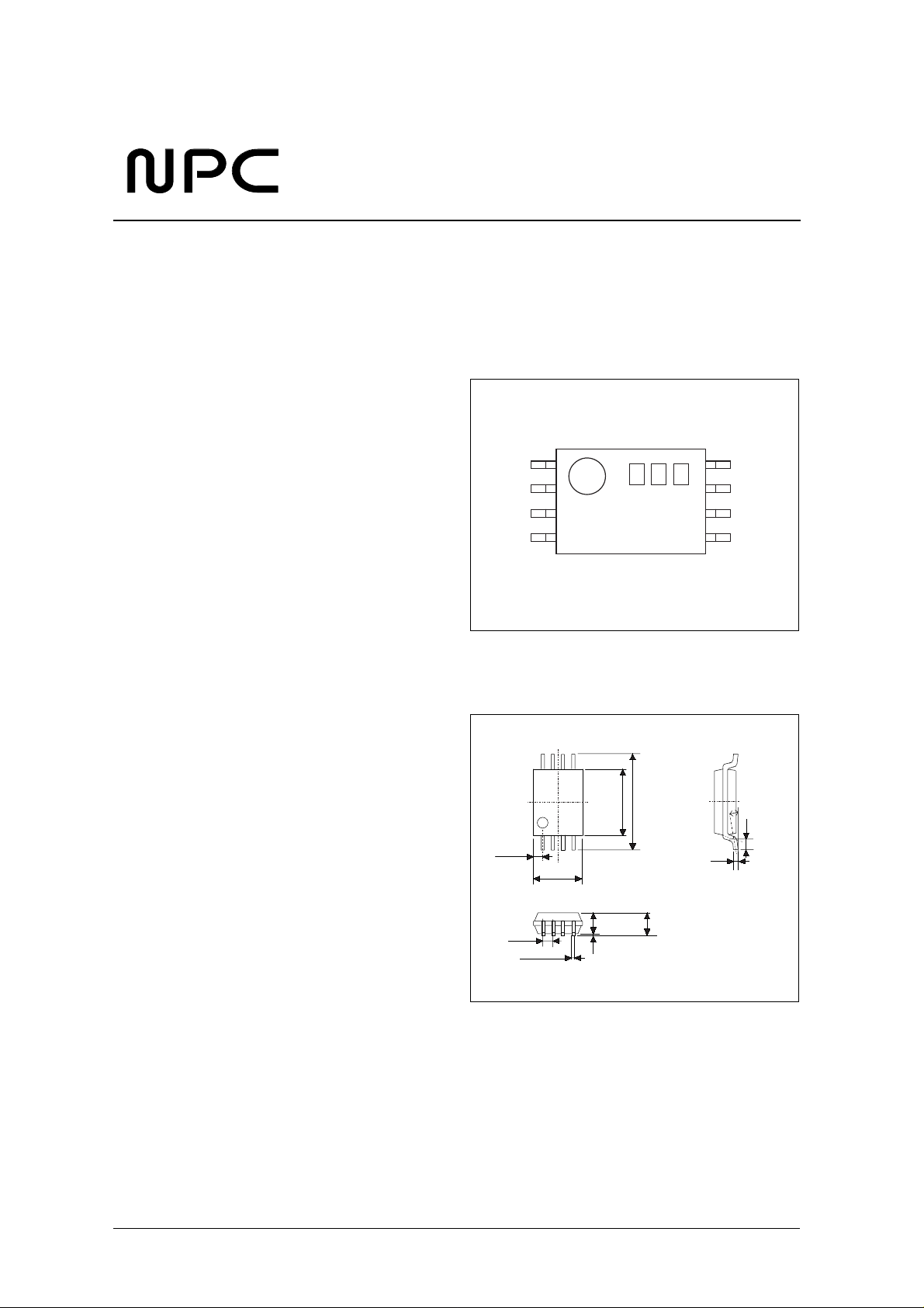
PINOUT
8-pin VSOP
Top view
INTN
XTN
XT
VSS
= date code
PACKAGE DIMENSIONS
Unit: mm
0.585 TYP
1
8578B
4
4.4±0.2
3.12±0.3
6.4±0.3
0.15
8
VDD
DATA
CLK
CE
5
0 to 10°
0.5±0.2
+0.1
-0.05
0.65
0.22±0.1
1.15±0.05
0.05±0.05
NIPPON PRECISION CIRCUITS—1
1.30 MAX
Page 2
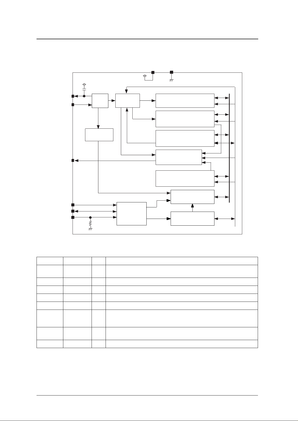
BLOCK DIAGRAM
SM8578BV
XTN
XT
INTN
CLK
DATA
CE
C
D
DETECT
OSC
OSC
DIVIDER
INPUT
CONTROLLER
VDD
INTERRUPT and FOUT
VSS
Control Line
CLOCK and CALENDAR
REGISTER
DIVIDER and
TIMER COUNTER
CONTROL REGISTER
CONTROLLER
ALARM REGISTER
SHIFT REGISTER
Internal Bus
CONTROL CIRCUIT
PIN DESCRIPTION
Number Name I/O Function
1 INTN O
2 XTN O Oscillator output. Oscillator capacitor C
3 XT I Oscillator input
4 VSS – Negative supply pin
5 CE I Chip enable. Chip is selected when HIGH. Pull-down resistor built-in
6 CLK I
7 DATA I/O
8 VDD – Positive supply voltage. A 0.1 µF pass capacitor should be connected between VDD and VSS.
Timer/alarm interrupt output and the setting frequency output,corresponding to the active internal mode.
N-channel open-drain output pin
built-in
D
Serial data clock.
In write mode, data is input on DATA on the rising edge of CLK.
In read mode, data is output on DATA on the rising edge of CLK.
Serial data input/output. When CE goes HIGH, initial 4-bit input data determines the device mode.
Subsequent data is transferred in write or read mode, as selected by the de vice mode.
NIPPON PRECISION CIRCUITS—2
Page 3
−
−
−
−
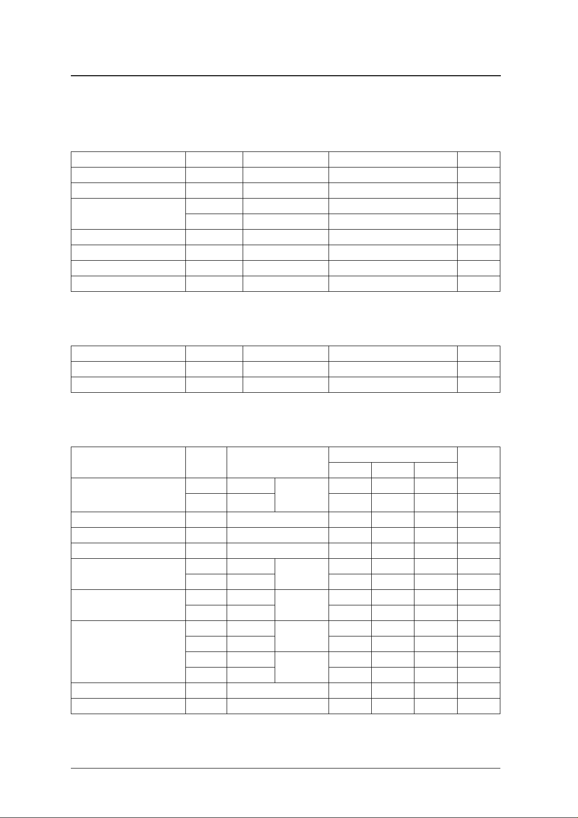
SPECIFICATIONS
Absolute Maximum Ratings
V
= 0 V
SS
Parameter Symbol Condition Rating Unit
Supply voltage range V
Input voltage range V
Output voltage range
Power dissipation P
Storage temperature range T
Soldering temperature T
Soldering time t
V
V
DD
OUT1
OUT2
STG
SLD
SLD
−
°
°
−
° C
−
SM8578BV
0.3 to 7.0 V
IN
All inputs V
INTN V
DATA V
D
SS
SS
0.3 to V
SS
0.3 to V
+ 0.3 V
DD
0.3 to 8.0 V
+ 0.3 V
DD
150 mW
55 to 125
255
10 s
C
C
Recommended Operating Conditions
V
= 0 V
SS
Parameter Symbol Condition Rating Unit
Supply voltage range V
Operating temperature range T
DD
opr
DC Electrical Characteristics
V
= 0 V, V
SS
Current consumption
HIGH-level input voltage V
LOW-level input voltage V
Input leakage current I
Input resistance
HIGH-level output voltage
LOW-level output voltage
Output leakage current I
Oscillator stop detection time t
= 1.6 to 5.5V , C
DD
= 10 pF, T
G
= − 40 to 85 ° C unless otherwise noted
a
Parameter Symbol Condition
I
I
LEAK
R
DWN1
R
DWN2
V
V
V
V
V
V
OSC
DD1
DD2
OH1
OH2
OL1
OL2
OL3
OL4
OZ
V
= 5.0 V CE = V
DD
V
= 3.0 V – 0.5 1.0 µA
DD
CE, CLK, DATA 0.8V
IH
CE, CLK, DATA 0 – 0.2V
IL
CE, CLK: V
V
= 5.0 V
DD
V
= 3.0 V 150 300 600 k Ω
DD
V
= 5.0 V
DD
V
= 3.0 V 2.0 – 3.0 V
DD
V
= 5.0 V
DD
V
= 3.0 V – – V
DD
V
= 5.0 V
DD
V
= 3.0 V – – V
DD
DATA, INTN: V
DATA, INTN =
V
DD
= V
IN
DD
CE: V
DATA: I
mA
DATA: I
mA
INTN: I
mA
OUT
= V
or V
IN
DD
OL
SS
SS
= V
OH
OL
= − 1
= 1
= 1
or V
DD
1.6 to 5.5 V
40 to 85
Rating
min typ m ax
– 1.0 2.0 µA
DD
–V
-0.5 – 0.5 µA
75 150 300 k Ω
4.5 – 5.0 V
––V
––V
SS
0.5 – 0.5 µA
10 – – ms
DD
DD
+ 0.5 V
SS
+ 0.8 V
SS
+ 0.25 V
SS
+ 0.4 V
SS
Unit
V
V
NIPPON PRECISION CIRCUITS—3
Page 4
Oscillator Characteristics
T
= 25 ° C, C
a
= 10 pF, Seiko Epson C-002SH crystal (C
G
SM8578BV
= 30 k Ω , C
I
= 6 pF) unless otherwise noted
L
−
−
Parameter Symbol Condition
Oscillator start time t
Oscillator stop voltage V
STA
STO
Frequency voltage characteristic f/V V
Frequency accuracy
Output capacitance C
ε
IC
D
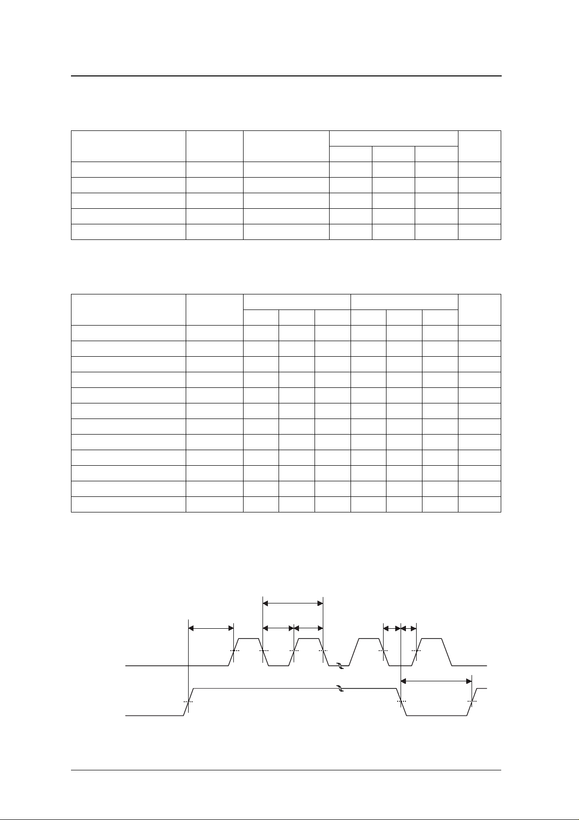
AC Characteristics
V
= 0 V, C
SS
CLK clock period t
CLK HIGH-level pulsewidth t
CLK LOW-level pulsewidth t
CE setup time t
CE hold time t
CE recovery time t
CLK hold time t
Write data setup time t
Write data hold time t
Read data output delay time
Output disable delay time
Input rise and fall time t
1. C
=50pF
L
2. C
=50pF, RL=10k Ω
L
= 50 pF, T
L
= − 40 to 85 ° C unless otherwise noted
a
Parameter Symbol
CLK
WH
WL
CS
CH
CR
CKH
DS
DH
1
2
t
RD
t
RZ
RF
Rating
min typ m ax
V
= 1.6 V – – 5.0 s
DD
Unit
– – 1.5 V
= 1.6 to 5.5 V
DD
V
= 5.0 V
DD
V
= 5.0 V – 15 – pF
DD
V
= 5 V ± 10% V
DD
2 – +2 ppm/V
10 – +10 ppm
= 3.0 V ± 1 0 %
DD
Unit
min typ ma x min typ ma x
600 – – 1200 – – ns
300 – – 600 – – ns
300 – – 600 – – ns
150 – – 300 – – ns
200 – – 400 – – ns
300 – – 600 – – ns
50 – – 100 – – ns
50 – – 100 – – ns
50 – – 100 – – ns
– – 200 – – 400 ns
– – 100 – – 200 ns
––20––40ns
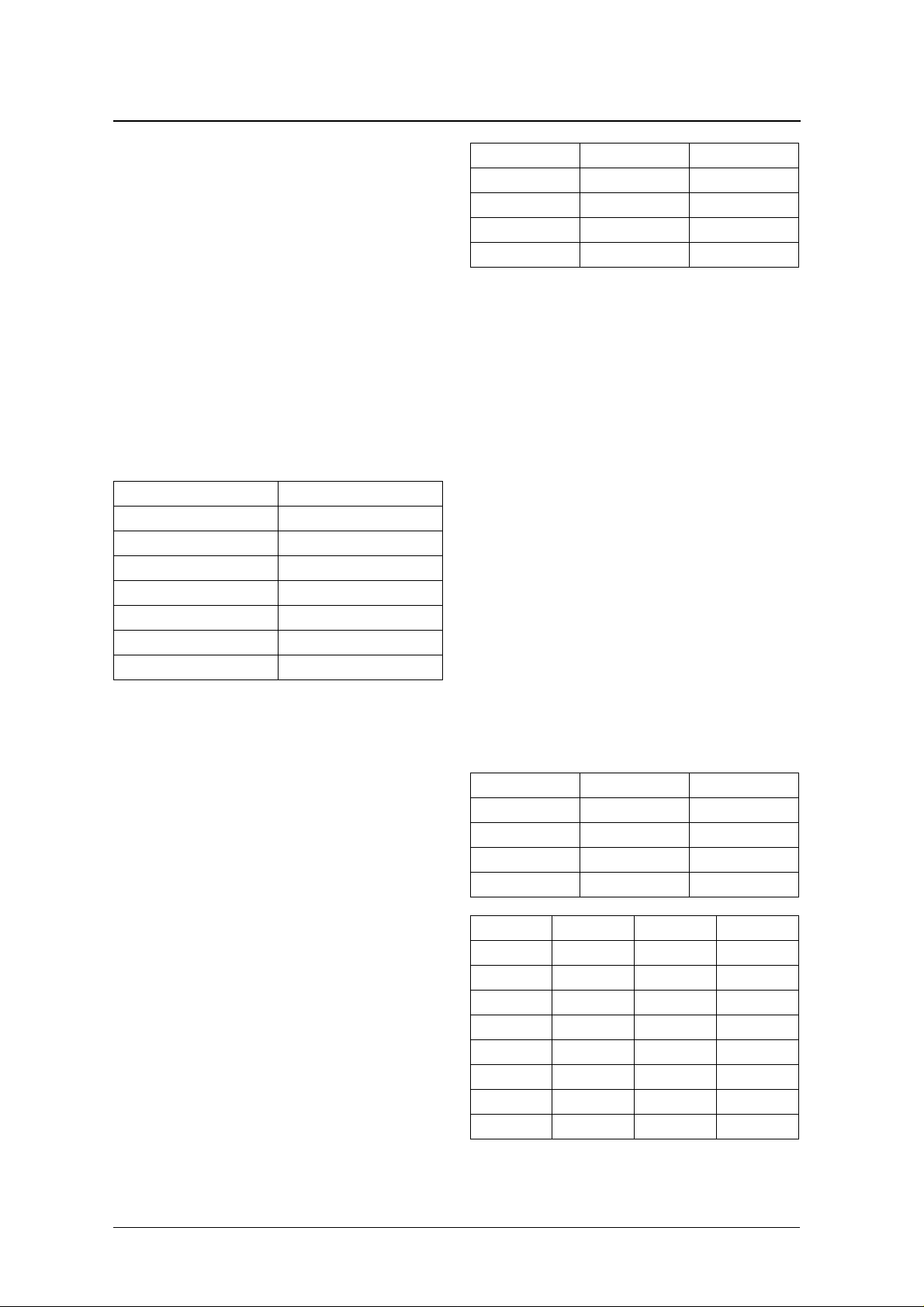
CLK
C E
50%
t
CS
50%
t
WL
t
CLK
t
WH
t
CHtCKH
t
CR
NIPPON PRECISION CIRCUITS—4
Page 5

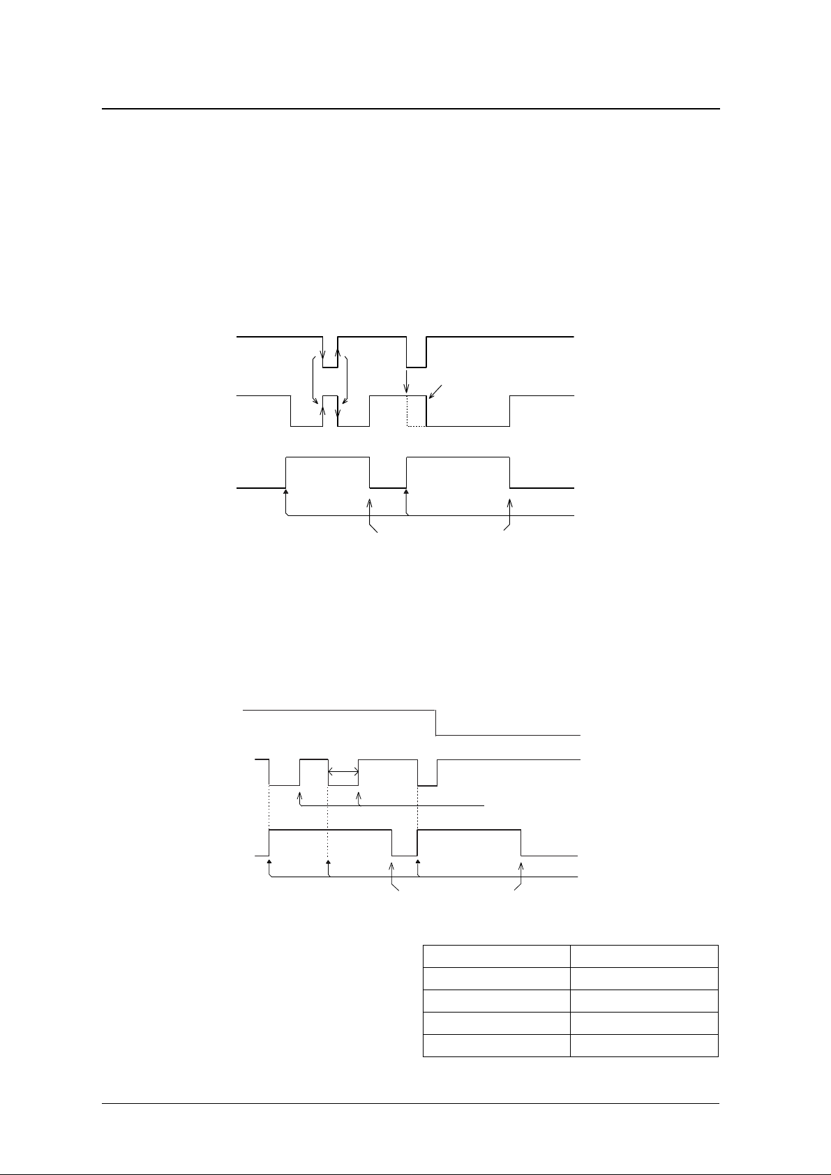
Data read
SM8578BV
t
RF
t
RF
Data write
CLK
DATA
C E
CLK
DATA
C E
50%
50%
50%
50%
t
RD
50%
50%
t
t
CS
DS
90%
10%
t
DH
90%
Hi-Z
10%
t
RZ
NIPPON PRECISION CIRCUITS—5
Page 6

FUNCTIONAL DESCRIPTION
Registers
SM8578BV
×
Addres
s
0 Second FOS 40 20 10 8421All bits All bits
1 Minute fr4020108421All bits All bits (excl. bit 7)
2 Hour fr
3 Weekday fr 6543210All bits All bits (excl. bit 7)
4Dayfr ×
5 Month fr
6 Year 804020108421All bits All bits
7 Minute alarm AE 40 20 10 8421All bits All bits
8 Hour alarm AE × 20108421All bits All bits
9 Weekday alarm AE 6543210All bits All bits
A Day alarm AE × 20108421All bits All bits
B Output frequency FE × FD4 FD3 × FD2 FD1 FD0 All bits All bits
C Cycle frequency TE × TD1 TD0 ××××All bits All bits
D Interval counter
E Control 1 ×××TI/TP AF TF AIE TIE All bits All bits
F Control 2 × TEST ×
Register
1
Bit 7 Bit 6 Bit 5 Bit 4 Bit 3 Bit 2 Bit 1 Bit 0 Readable Writable
20108421All bits All bits (excl. bit 7)
20108421All bits All bits (excl. bit 7)
×× 108421All bits All bits (excl. bit 7)
2
1286432168421All bits All bits
RESE
HOLD ×××All bits All bits
T
3
1. When power is applied, all register values are undefined. Accordingly, all registers must be set by initial input data.
2. When address D is read, the previous preset data value is output.
3. Bits AF and TF can only be set to 0 by writing to address E (i.e. reset only).
× = don’t care. All don’t care bits can be used as general-purpose RAM.
Clock and calendar registers (address 0 to 6)
Data in these registers is interpreted in BCD format.
For example, if the second register contains
0101 1001, then the contents of the register is interpreted as the value 59 seconds. Hour register contents are values expressed in 24-hour mode.
Bit 6 Bit 5 Bit 4 Bit 3 Bit 2 Bit 1 Bit 0 W eekday
0010000Thursday
0100000 Friday
1000000Saturday
Leap-year detection is made by dividing the year
register contents (2 BCD digits) by 4. If the remainder is 0, corresponding to a leap year, the values in
the weekday and day registers are adjusted automatically. Note that the year following year 99 is year 00.
The FOS bit is the oscillator stop flag. It indicates
that the oscillator has stopped due to output voltage
reduction during operation. It is set to 1 when the
oscillator stops, and remains 1 until reset by writing
0 to FOS. It is not affected by the function of other
The weekday register contains values representing
bits.
the day of the week as shown in the following table.
Note that software measures should be taken to
ensure that only one bit is set to 1.
The fr bits are the read flags. They indicate that the
contents of the corresponding register generated an
overflow bit while a read cycle was in progress (CE
Bit 6 Bit 5 Bit 4 Bit 3 Bit 2 Bit 1 Bit 0 W eekday
0000001 Sunday
0000010Monday
0000100Tuesday
0001000Wednesday
= HIGH). If any fr bit encountered is set to 1, then all
clock timer registers must be read again. The fr bits
are cleared to 0 when CE goes LOW.
The seconds and year registers do not have fr bits to
indicate overflow. Instead, the value of the two most
significant bits (bits 5 and 6 in the seconds register,
NIPPON PRECISION CIRCUITS—6
Page 7
SM8578BV
and bits 6 and 7 in the year register) are set to 1 (for
example, Y ear: 0010 1001 → 1110 1001). The illegal
value that results can then be used to indicate overflow, serving the same function as an fr flag. The correct value of the register is restored when CE goes
LOW.
Alarm registers (address 7 to A)
An alarm can be set for day, weekday, hour and
minute. The weekday alarm register settings correspond to the weekdays as shown in the following
table. The alarm setting can also be set for more than
one weekday by setting more than one bit to 1. Note
that if a weekday alarm is set, then the hour alarm,
minute alarm or both should be set; the alarm may
not be output correctly if only a weekday alarm is
set.
Ad dress 9 Weekday
Bit 0 = 1 Sunday
Bit 1 = 1 Monday
Bit 2 = 1 Tuesday
Bit 3 = 1 Wednesday
Bit 4 = 1 Thursday
Bit 5 = 1 Friday
Bit 6 = 1 Saturday
Bit 7 of each of the alarm registers is an alarm enable
bit (AE). When AE is 0, the register contents are
compared with the corresponding clock timer register contents to determine when the alarm condition
has occurred. When AE is 1, all data bits in the register are considered as don’t care bits. In this case, the
data is ignored and the alarm condition is always
active for all valid values of that register. Thus AE
can be used to set regular alarms, such as hourly or
daily alarms regardless of the current hour or day.
When the alarm interrupt enable bit (AIE) in register
address E is 0, alarm output on INTN is disabled.
TIE and FE must be set to 0, and AIE set to 1 to
enable the alarm interrupt function.
Timer registers (address C to E)
The timer registers control an 8-bit presettable downcounter. The timer counter in register address D
counts down using the source clock frequency
assigned by bits TD0 and TD1 in register address C,
as shown in the following table. When the counter
becomes zero, generating a timer interrupt event,
INTN goes LOW. The counter is then reloaded with
the preset count and count down starts again. Thus
the timer counter is used as an interval timer.
TD0 TD1 Source clock
0 0 4096 Hz
0 1 64 Hz
1 0 1 Hz (1 s)
1 1 1/60 Hz (1 min)
When the timer interrupt enable bit (TIE) in register
address E is 0, timer output on INTN is disabled.
AIE and FE must be set to 0, and TIE set to 1 to
enable the timer interrupt function. TI/TP controls
the timer output mode.
The presettable down-counter is loaded with new
data whenever a write to register address D occurs.
Note that when the timer interrupt is disabled (TIE =
0), the data in register address D is stored and thus
register address D can be used as general-purpose
RAM, just as described for the don’t care bits in the
register table.
When the timer enable bit (TE) is 0, the timer
counter data is loaded into the counter. The count is
then started by setting TE to 1.
Output frequency register (address B)
The output frequency on INTN is determined by the
frequency divider ratio set by FD0 to FD2 and by the
source clock frequency set by FD3 and FD4, as
shown in the following tables. AIE and TIE should
be 0 when setting the output frequency. When the
frequency output enable bit (FE) is 0, INTN is in a
high-impedance state.
FD4 FD3 Source clock
0 0 32768 Hz
0 1 1024 Hz
1 0 32 Hz
1 1 1 Hz
FD 2 FD 1 FD 0 Divider ratio
0001/1
0011/2
0101/3
0111/6
1001/5
1 0 1 1/10
1 1 0 1/15
1 1 1 1/30
NIPPON PRECISION CIRCUITS—7
Page 8

SM8578BV
Control register 1 (address E)
This register comprises the alarm interrupt and timer
interrupt control flags.
Ad dres
Bit 7 Bit 6 Bit 5 Bit 4 Bit 3 Bit 2 Bit 1 Bit 0
s
E ×××TI/TP AF T F AIE TIE
The TI/TP bit is an interrupt signal output mode
select (interrupt/periodic) bit. In timer mode, FE and
AIE should be set to 0.
When TI/TP is 0, level interrupt mode is selected. In
this mode (TI/TP = 0 and TIE = 1), INTN goes LOW
and TF is set to 1 when a timer interrupt event
occurs. INTN remains LOW until 0 is written to TF.
When TI/TP is 1, repetitive interrupt (interval) mode
is selected. In this mode (TI/TP = 1 and TIE = 1),
INTN goes LOW and TF is set to 1 when a timer
interrupt event occurs. INTN then goes into a highimpedance state after a preset auto-return time set by
the source clock. TF remains 1 until 0 is written to
TF.
Control register 2 (address F)
This register comprises the frequency divider control
bits for the timers.
The AF and TF bits are the alarm flag and timer flag,
respectively. AF is set to 1 when an alarm event
occurs, and TF is set to 1 when the timer downcounter drops to zero. When set they remain 1 until 0
is written to the respective bit. Neither bit can be
written to with 1 data.
The AIE and TIE bits are the alarm interrupt enable
and timer interrupt enable bits, respectively. When
enabled and a corresponding alarm or timer interrupt
event occurs, INTN output becomes active. Alarm
and timer interrupts are enabled by writing 1 to the
corresponding interrupt enable bit. Note that both
interrupt enable bits should not be simultaneously set
to 1.
Ad dres
Bit 7 Bit 6 Bit 5 Bit 4 Bit 3 Bit 2 Bit 1 Bit 0
s
F × TEST ×
RESE
HOLD ×××
T
The TEST bit is an NPC factory test bit. It should be
set to 0 when power is applied and when writing to
register address F.
The RESET bit is the counter reset bit. When
RESET is 1, the 1 Hz to 2 kHz frequency divider
counters are reset and clock functions are reset.
RESET is cleared by either writing 0 or automatically when CE goes LOW. It is not affected by the
settings of any other bits.
The HOLD bit is the clock function stop bit. When
HOLD is 1, the seconds register digit is not incremented. If, however, an increment event would have
occurred, the digit is incremented when HOLD is set
to 0. Accordingly, HOLD should be set to 1 for periods of less than one second to maintain correct timing.
NIPPON PRECISION CIRCUITS—8
Page 9

Interrupt Operation
Interrrupt output
SM8578BV
The INTN interrrupt output mode is determined by
the timer interrupt bit (TIE), alarm interrupt bit
(AIE), and frequency enable bit (FE), as shown in
the following table. Note that only one bit can be set
to 1.
Alarm interrupt
When AIE is 1 and an alarm e v ent occurs, INTN output goes LOW. If AIE is 0, however, INTN is in a
high-impedance state. The alarm interrupt is output
AIE bit
INTN output
AF bit
TIE AIE FE MODE
1 0 0 Timer interrupt output
0 1 0 Alarm interrupt output
0 0 1 Frequency output
0 0 0 Output disabled
when a carry from the seconds register to the minute
register occurs.
"1"
"0"
No output while AIE is 0
Hi-Z
LOW-level
"1"
"0"
Data 0 written to AF
Alarm interrupt
timing
NIPPON PRECISION CIRCUITS—9
Page 10
SM8578BV
Timer interrupt
The timer interrupt mode (level interrupt or repetitiv e
interrupt) is selected by the setting of TI/TP. In timer
mode, AIE and FE should be set to 0.
Level interrupt mode (TI/TP = 0)
When TIE is 1 and a timer interrupt event occurs,
INTN goes LOW and TF is set to 1. INTN goes into
a high-impedance state when 0 is written to TF.
TIE bit
INTN output
TF bit
Data 0 written to TF
Repetitive interrupt mode (TI/TP = 1)
When TIE is 1 and a timer interrupt event occurs,
INTN goes LOW and TF is set to 1. INTN then goes
into a high-impedance state after the auto-return
When TIE is 0, however, INTN is in a high-impedance state.
"1"
No output
while TIE is 0
"0"
Hi-Z
LOW-level
"1"
"0"
Timer interrupt
timing
time. TF remains 1 until 0 is written to TF. When TIE
is 0, however, INTN is in a high-impedance state.
TIE bit
tRTN
INTN output
TF bit
The auto-return time (t
) is determined by the
RTN
source clock frequency set by register address C as
shown in the following table.
Auto-return
Data 0 written to TF
Source clock Auto-return time (t
4096 Hz 0.122 ms
64 Hz 7.81 ms
1 Hz 0.5 s
1/60 Hz 0.122 ms
"1"
"0"
Hi-Z
LOW-level
"1"
"0"
Timer interrupt
timing
)
RTN
NIPPON PRECISION CIRCUITS—10
Page 11

Addressing
SM8578BV
When CE goes HIGH for either a read or write cycle,
the initial input data comprises 4 mode select bits
followed by 4 address bits. Subsequent data is
read/written (depending on the mode selected) in 8-
Write cycle
When the first 4 bits of input data after CE goes
HIGH is 3H, write mode is selected. The subsequent
4 bits select the address to be written. The next 8 bits
of data are then written to the selected address, and
C E
CLK
DATA
D0 D1 D2 D3 D0 D1 D4 D5D2 D3 D2 D3 D6 D7
Write mode
select code(3
D0 D1 D0 D1 D4 D5D2 D3 D6 D7
Adress
select(N)
H)
Data WRITE(adress N)
bit units from/to the address selected. All input/output data is in LSB-first format.
Note that if CE goes LOW before a complete 8-bit
unit of input data, the entire 8 bits of data are
ignored.
then the address is automatically incremented. Subsequent input data is written to addresses in increasing order. Note that the address following address F
is address 0H.
DATA WRITE(adress N+1)
H
Read cycle
When the first 4 bits of input data after CE goes
HIGH is CH, read mode is selected. The subsequent
4 bits select the address to be read. 8-bit is then read
from the selected address, and then the address is
C E
CLK
D0 D1
DATA
D2 D3 D0 D1 D2 D3
Read mode
select code(C
Adress
select(N)
H
)
D0 D1 D2 D3 D4 D5 D6 D7 D0 D1 D2 D3 D4 D5
Data read(adress N)
From the point DATA is in output mode.
Note that if a mode select code other than 3H or C
is input, all following data is ignored until a valid
mode select code occurs.
automatically incremented. Subsequent input data is
read from addresses in increasing order. Note that the
address following address FH is address 0H.
D6 D7
DATA read(adress N+1)
H
NIPPON PRECISION CIRCUITS—11
Page 12

Setting the Alarm
SM8578BV
Alarms can be set for day, weekday, hour and
minute. An alarm can also be set for more than one
weekday. Note that it is recommended that AF and
AIE be set to 0 to avoid accidental hardware interrupts while setting the alarm.
After the alarm data is entered, initialization occurs
when AF is again set to 0. The alarm interrupt is
enabled by writing 1 to AIE.
If the hardware interrupt is not used, then AIE should
be set to 0. In this case, an alarm can still be controlled by software monitoring of AF using read
cycles.
Example 1
To set an alarm for 6pm of the following day:
• Set bits AIE and AF to 0.
Monitoring Oscillator Frequency
• Set the day register AE bit to 1 (don’t care).
• Acquire the current weekday setting from register address 3, rotate result left by 1 bit, and
write to weekday alarm register (while monitoring the fr bit).
• Write 18
to the hour alarm register.
H
• Write 00H to the minute alarm register.
• Set AF to 0 and AIE to 1.
Example 2
To set an alarm for 6am for Monday to Friday:
• Set bits AIE and AF to 0.
• Set the day register AE bit to 1 (don’t care).
• Write 3EH to the weekday alarm register.
• Write 06H to the hour alarm register.
• Write 00H to the minute alarm register.
• Set AF to 0 and AIE to 1.
C1
R1
R2
CG
SW
XTN
XT
VDD
CE
VSS
R3
INTN
INTN output (1Hz)
R1=R2 =10kΩ (typ.)
R3=10kΩ (typ.)
C1=0.1µF (typ.)
NIPPON PRECISION CIRCUITS—12
Page 13

APPLICATION CIRCUIT
SM8578B
VDD
SM8578BV
VCC
VCC
INTN
XT
XTN
VSS
CE
CLK
DATA
Micro
controller
GND
NIPPON PRECISION CIRCUITS INC. reserves the right to make changes to the products described in this data sheet in order to
improve the design or performance and to supply the best possible products. Nippon Precision Circuits Inc. assumes no responsibility for
the use of any circuits shown in this data sheet, conveys no license under any patent or other rights, and makes no claim that the circuits
are free from patent infringement. Applications for any devices shown in this data sheet are for illustration only and Nippon Precision
Circuits Inc. makes no claim or warr anty that such applications will be suitab le for the use specified without further testing or modification.
The products described in this data sheet are not intended to use for the apparatus which influence human lives due to the failure or
malfunction of the products. Customers are requested to comply with applicable laws and regulations in effect now and hereinafter,
including compliance with export controls on the distribution or dissemination of the products. Customers shall not expor t, directly or
indirectly, any products without first obtaining required licenses and approvals from appropriate government agencies.
NIPPON PRECISION CIRCUITS INC.
4-3, Fukuzumi 2-chome
Koto-ku, Tokyo 135-8430, Japan
NIPPON PRECISION CIRCUITS INC.
Telephone: 03-3642-6661
Facsimile: 03-3642-6698
NC9619CE 1997.08
NIPPON PRECISION CIRCUITS—13
 Loading...