

Page 1
SM8577B
NIPPON PRECISION CIRCUITS INC.
OVERVIEW
The SM8577B is a CMOS serial-interface type realtime clock IC that operates at 32.768 kHz. It
employs a 3-line serial interface to transfer time and
date data. It incorporates a supply-voltage detect
function to determine data validity/invalidity. It
features an output interrupt with 32 kHz or 1 Hz
output frequency. It is available in 8-pin SOPs.
FEATURES
■
2.5 to 5.5 V operating voltage range
■
1.0 µA at 3.0 V (typ) current consumption
■
3-line serial interface
■
1.7 ± 0.3 V supply voltage detection threshold
■
Timer counters for second, minute, hour, day, day
of the week, month, and year
■
Automatic leap-year calendar adjustment
■
32.768 kHz and 1 Hz output interrupt selectable
■
Crystal oscillator circuit built-in (C
■
24-hour time mode
■
8-pin SOP
built-in)
D
Real-time Clock IC
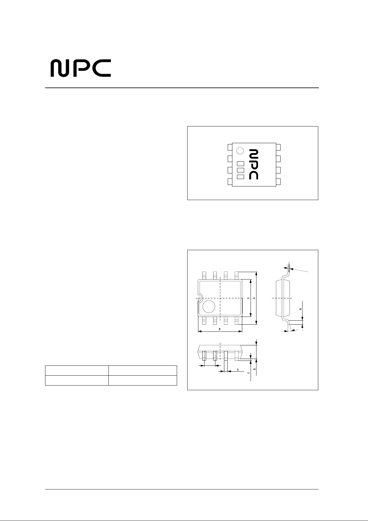
PINOUT
1
CE
DATA
CLK
FOUT
4
PACKAGE DIMENSIONS
Unit: mm
8-pin SOP
8577B
8
VDD
XTN
XT
5
VSS
+ 0.10
0.15
− 0.05
ORDERING INFOMATION
Device Package
SM8577BS 8pin SOP
1.27
5.2 0.3
0.4 0.1
4.4 0.2
6.2 0.3
1.5 0.1
0.05 0.05
4.4 0.2
0 to 10∞
NIPPON PRECISION CIRCUITS—1
Page 2
≥
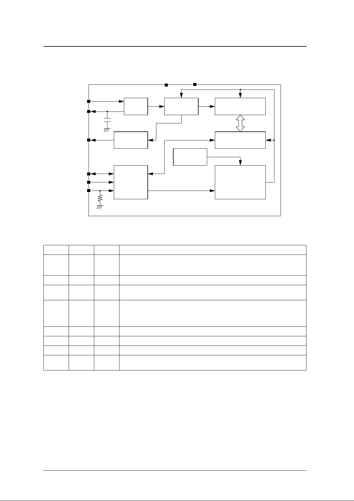
BLOCK DIAGRAM
SM8577B
VDD VSS
XT
OSC
Divider Timer Counter
XTN
FOUT
Output
Controller
Voltage
Detect
DATA
CLK
CE
I/O
Controller
PIN DESCRIPTION
Number Name I/O Description
1CEI
2 DATA I/O Data read and write input/output
3 CLK I
4 FOUT O
5 VSS – Ground
6 XT I Crystal oscillator element connection pin
7 XTN O Crystal oscillator element connection pin. Oscillator capacitor C
8 VDD –
Chip enable. With pull-down resistor built-in.
HIGH: Enable
LOW: DATA goes high impedance; input on CLK and DATA stops; and the TM bit is cleared.
Serial clock input.
Data is input (write mode) and output (read mode) on the rising edge of CLK.
Frequency output (controlled by the 4th data bit of the ‘week’ data, FSEL).
1 Hz output when FSEL is 0, and 32.768 kHz output when FSEL is 1.
In 1 Hz output mode, the 1 Hz signal is synchronized to the internal 1 second signal.
FOUT output is not affected by the CE signal.
Supply voltage.
Connect a
0.1 µF capacitor between VDD and VSS.
Shift Register
Controll
Circuit
is built-in.
D
NIPPON PRECISION CIRCUITS—2
Page 3
−
−
−
SPECIFICATIONS
Absolute Maximum Ratings
V
= 0 V
SS
Parameter Symbol Condition Rating Unit
Supply voltage range V
Input voltage range V
Output voltage range V
Storage temperature range T
Power dissipation P
Soldering temperature T
Soldering time t
−
°
°
−
° C
−
ε
−
SM8577B
DD
IN
OUT
stg
D
sld
sld
0.3 to 7.0 V
V
0.3 to V
SS
V
0.3 to V
SS
+ 0.3 V
DD
+ 0.3 V
DD
55 to 125
150 mW
255
10 s
C
C
Recommended Operating Conditions
V
= 0 V
SS
Parameter Symbol Condition Rating Unit
Supply voltage range V
Operating temperature range T
DD
opr
Oscillator Characteristics
V
= 0 V, T
SS
noted
Oscillator start time t
Oscillator start voltage V
Oscillator stop voltage V
Frequency voltage characteristic f/V V
Frequency accuracy
Output capacitance C
= 25 ° C, C
a
= 12 pF, Seiko Epson C-002SH crystal (C
G
Parameter Symbol Condition
STA
STA
STO
D
V
DD
DD
V
DD
V
DD
2.5 to 5.5 V
40 to 85
= 30 k Ω , C
I
= 6 pF) unless otherwise
L
Rating
Unit
min typ m ax
= 2.5 V – – 3 s
1.5 – – V
– – 1.5 V
= 2.0 to 5.5 V
= 5.0 V
2 – +2 ppm/V
10 – +10 ppm
= 5.0 V – 12 – pF
NIPPON PRECISION CIRCUITS—3
Page 4

DC Electrical Characteristics
V
= 0 V, V
SS
= 5.0 V ± 10%, T
DD
= − 40 to 85 ° C unless otherwise noted
a
SM8577B
−
−
Parameter Symbol Condition
Current consumption
HIGH-level input voltage V
LOW-le v el input voltage V
Input resistance R
Input OFF leakage current I
HIGH-level output voltage
LOW-level output voltage
Output leakage current
Supply voltage detect threshold
voltage
V
V
V
V
V
I
DD1
I
DD2
leak
OH1
OH2
OL1
OL2
I
OZH
I
OZL
DET
min typ m ax
V
= 5.0 V
DD
V
= 3.0 V – 1.0 2.0 µA
DD
CE, CLK, DATA 0.8V
IH
CE, CLK, DATA – – 0.2V
IL
CE: V
IN
IN
CLK: V
CE: V
IN
V
= 5.0 V
DD
V
= 3.0 V 2.0 – – V
DD
V
= 5.0 V
DD
V
= 3.0 V – – V
DD
DATA, FOUT: V
DATA, FOUT: V
CE = V
SS
= 5.0 V – – 800 k Ω
= V
or V
IN
DD
= V
SS
SS
DATA, FOUT:
I
= − 1.0 mA
OH
DATA, FOUT:
I
= 1.0 mA
OL
= 5.5 V
OUT
= 0 V
OUT
– 1.5 3.0 µA
DD
– – 0.5 µA
4.5 – – V
––V
1.0 – 1.0 µA
1.0 – 1.0 µA
1.4 1.7 2.0 V
Rating
Unit
––V
DD
+ 0.5 V
SS
+ 0.8 V
SS
V
NIPPON PRECISION CIRCUITS—4
Page 5

AC Characteristics
V
= 5 V ± 10%, V
DD
SS
= 0 V, T
= − 40 to 85 ° C, C
a
SM8577B
= 50 pF unless otherwise noted
L
Parameter Symbol Condition
CLK clock period t
CLK LOW-level pulsewidth t
CLK HIGH-level pulsewidth t
CE setup time t
CE hold time t
CE enable time t
Write data setup time t
Write data hold time t
DATA output delay time t
DATA output floating time t
Clock rise time t
Clock f all time t
FOUT rise time t
FOUT fall time t
CLK
CLKL
CLKH
CES
CEH
CE
SD
HD
DATD
DZ
r1
f1
r2
f2
FOUT duty cycle Duty C
Wait time t
RCV
Rating
min max min
Unit
0.75 – 7800 µs
0.375 – 3900 µs
0.375 – 3900 µs
0.375 – 3900 µs
0.375 – – µs
– – 0.9 s
0.1 – – µs
0.1 – – µs
– – 0.2 µs
See measurement circuit. – – 0.1 µs
––50ns
––50ns
C
= 30 pF – – 100 ns
L
C
= 30 pF – – 100 ns
L
= 30 pF, 32 kHz output 40 – 60 %
L
0.95 – – µ s
V
= 3 V ± 10%, V
DD
= 0 V, T
SS
= − 40 to 85 ° C, C
a
Parameter Symbol Condition
CLK clock period t
CLK LOW-level pulsewidth t
CLK HIGH-level pulsewidth t
CE setup time t
CE hold time t
CE enable time t
Write data setup time t
Write data hold time t
DATA output delay time t
DATA output floating time t
Clock rise time t
Clock f all time t
FOUT rise time t
FOUT fall time t
CLK
CLKL
CLKH
CES
CEH
CE
SD
HD
DATD
DZ
r1
f1
r2
f2
FOUT duty cycle Duty C
Wait time t
RCV
= 50 pF unless otherwise noted
L
Rating
Unit
min max min
1.5 – 7800 µs
0.75 – 3900 µs
0.75 – 3900 µs
0.75 – 3900 µs
0.75 – – µ s
– – 0.9 s
0.2 – – µs
0.1 – – µs
– – 0.4 µs
See measurement circuit. – – 0.2 µs
– – 100 ns
– – 100 ns
C
= 30 pF – – 200 ns
L
C
= 30 pF – – 200 ns
L
= 30 pF, 32 kHz output 40 – 60 %
L
1.9 – – µs
NIPPON PRECISION CIRCUITS—5
Page 6

Measurement Circuit
VDD
VSS
DATA Output Floating Timing
DATA
CE
SM8577B
SW2
10kΩ
Output
10kΩ
SW1 50pF
P.G
CE
DATE
CE
DATA
tDHZ
50%
90%
tDLZ
50%
10%
NIPPON PRECISION CIRCUITS—6
Page 7

Timing Diagrams
Data read
CE
CLK
DATA
Data write
tCES
tCLK
tCLKH
tCLKL tr1tf1
tDATD
SM8577B
t
CE
tCEH
tRCV
tDZ
CE
CLK
DATA
FOUT output
FOUT
tsD
tCES
tCLKH
tCLK
tCLKL
tHD
10%
t
CE
tCEH tRCV
tf1
tr1
tr2
90%
t
r2
t
tH
50%
tH
Duty= X 100(%)
t
Note that the 1 Hz and 32 kHz oscillators are not
synchronized to each other, so switching between 1
Hz and 32 kHz output temporarily shortens the duty
cycle. Accordingly, a wait time (≥ output frequency
period) should be incorporated when switching
during normal operation.
NIPPON PRECISION CIRCUITS—7
Page 8

FUNCTIONAL DESCRIPTION
Timer Data Configuration
SM8577B
Counter data is stored in BCD format. The IC
performs long/short month and leap-year adjustment
automatically. Leap-year adjustment occurs:
• when the decade digit is odd and the year digit
is a 2 or 6, and
MSB LSB
Second ( 0 to 59 )
Minute ( 0 to 59 )
Hour ( 0 to 23 )
Week ( 1 to 7 )
Day ( 1 to 31 )
FDT
∗
∗ ∗
∗ ∗
s40 s20 s10 s8 s1s2s4
mi40 mi20 mi10 mi8 mi1mi2mi4
• when the decade digit is even and the year digit
is a 0, 4 or 8.
The time display is 24-hour mode. All data is written
and read with the LSB first.
h20 h10 h8 h1h2h4
FSEL
d20 d10 d8 d1d2d4
W1W2W4
Month ( 1 to 12 )
Year ( 0 to 99 )
TM
y80 y40 y20 y10 y8 y1
∗
* bits are don’t care write bits.
FDT is the supply voltage detect bit. FDT is set to 1
when the voltage between VDD and VSS falls below
1.7 ± 0.3 V. It is reset to 0 for data reads longer than
56 bits. Note that the FDT bit is not reset to 0 for
data reads of 55 bits or less. The read/write data bits
should initially be set to 0. After the supply v oltage is
first applied, the FDT bit should also be set to 0.
∗
mo10 mo8 mo1mo2mo4
y4
y2
FSEL is the FOUT output frequency switch control
bit. 1 Hz output is selected when FSEL is 0, and 32
kHz output is selected when FSEL is 1. After power
is first applied, 1 Hz default mode is selected.
TM is the factory test bit. It should be set to 0 for
normal use.
NIPPON PRECISION CIRCUITS—8
Page 9

Data Read
CE
SM8577B
123
89
CLK
DATA
Don't Care
Control Bits
Data Input Mode
When CE is HIGH, data read mode starts from the
first rising edge of CLK for which DATA is LOW.
Valid data is then output on DATA from the 9th
rising edge of CLK. Time and date data is loaded
into the shift register on the 8th falling edge of CLK
and then output on DATA in sync with the rising
edge of CLK, starting with the seconds’ digit LSB.
Data is loaded and shifted in the sequence second,
minute, hour, week, day, and month. The output data
is valid for the first 60 rising edges of CLK. Output
data does not change after the 60th rising edge, even
if clock input continues.
10 11
58 59
60
60+n
Output data
not change
s1
s2 s4 y20
Second
y40 y80
Year
Data Output Mode
corresponding number of cycles. For example, if
only the ‘second’ to ‘week’ data output is required,
then that data only is output if CE goes LOW after 36
clock cycles.
For continuous data reads, a wait time (t
required before the next data cycle after CE goes
LOW.
Note that if a timer counter update operation (a 1 s
carry) occurs during a data read cycle, the data in the
shift register is not updated and, as a result, the
output data contains an error of −1 s.
RCV
) is
Within the 60 cycles of valid data output, partial data
output can be obtained by taking CE LOW after the
Data Write
CE
1
23
89
CLK
DATA
Don′t Care
Control Bits
Data Input Mode
The data read cycle should be completed within
tCE ≤ 0.9 s.
10 11
s1
s4 y20 y40 y80
s2
58 59
Second
60
Year
Data Input Mode
60+n
NIPPON PRECISION CIRCUITS—9
Page 10

SM8577B
When CE is HIGH, data write mode starts from the
first rising edge of CLK for which DATA is HIGH.
Valid data is then input on DATA from the 9th rising
edge of CLK. Time and date data is loaded into the
shift register in sync with the rising edge of CLK,
starting with the seconds’ digit LSB. Data is loaded
and shifted in the sequence second, minute, hour,
week, day, and month. After 60 rising edges of CLK,
the shift register contents are then transferred to the
timer counters.
Note that a data write cycle must contain 60 bits of
input data. If CE goes LOW before 60 bits are input,
the input data is invalid. If the input data exceeds 60
bits, data from the 61st bit is ignored (the first 60 bits
remain valid).
Supply V oltage Detection
The supply voltage detector tests the level of the
supply voltage once every 0.5 seconds. If the supply
voltage falls below the detector threshold, the FDT
bit is set to 1. The FDT bit is reset to 0 after a data
During a data write cycle, timer counter operation
stops on the first falling edge of CLK, and the 1 Hz
to 128 Hz frequency divider step counters are reset.
The 1 s counter increment signal is stopped and does
not restart until CE goes LOW. The divider step
counters are reset during the interval between the
first falling edge of CLK and the 2nd rising edge of
CLK.
The data write cycle should be completed within
t
≤ 0.9 s.
CE
If a data read cycle occurs immediately after a data
write cycle, a wait time (t
) is required after CE
RCV
goes LOW.
Note that activating a read cycle when no valid data
is present will cause incorrect operation. All bits
must be valid data bits.
read cycle that contains at least 56 data bits. The
FDT bit is not reset for data read cycles of 55 bits or
less.
VDD
V
DET
0.5 second 0.5 second
Detected Pulse
CE
(READ MODE)
FDT bit
NIPPON PRECISION CIRCUITS INC. reserves the right to make changes to the products described in this data sheet in order to
improve the design or performance and to supply the best possible products. Nippon Precision Circuits Inc. assumes no responsibility for
the use of any circuits shown in this data sheet, conveys no license under any patent or other rights, and makes no claim that the circuits
are free from patent infringement. Applications for any devices shown in this data sheet are for illustration only and Nippon Precision
Circuits Inc. makes no claim or warr anty that such applications will be suitab le for the use specified without further testing or modification.
The products described in this data sheet are not intended to use for the apparatus which influence human lives due to the failure or
malfunction of the products. Customers are requested to comply with applicable laws and regulations in effect now and hereinafter,
including compliance with export controls on the distribution or dissemination of the products. Customers shall not expor t, directly or
indirectly, any products without first obtaining required licenses and approvals from appropriate government agencies.
NIPPON PRECISION CIRCUITS INC.
NIPPON PRECISION CIRCUITS INC.
4-3, Fukuzumi 2 chome
Koto-ku, Tokyo 135-8430, Japan
Telephone: 03-3642-6661
Facsimile: 03-3642-6698
NC9617AE 1997.04
NIPPON PRECISION CIRCUITS—10
 Loading...