

Page 1

- 1 -
SM8521 CONTENTS
DESCRIPTION
..............................................................
2
FEATURES
....................................................................
2
PIN CONNECTIONS
.....................................................
3
BLOCK DIAGRAM
.......................................................
4
PIN DESCRIPTION
.......................................................
5
ABSOLUTE MAXIMUM RATINGS
.............................
6
RECOMMENDED OPERATING CONDITIONS
.............
6
DC CHARACTERISTICS
.............................................
7
SM85CPU
......................................................................
8
Register Lineup
Address Space
ROM Area
Register File Area
RAM Area
Data Format
Bus Timing
SYSTEM CONTROL
..................................................
18
Oscillator Circuit
Clock System
Memory Map
Hardware Reset
Interrupt Function
Standby Function
I/O PORTS
...................................................................
29
TIMER/COUNTERS
....................................................
30
Clock Timer
Watchdog Timer Register (WDT)
LCDC/DMA
..................................................................
33
VRAM Configuration
DMA Transfer
Compound and Overwrite Mode
Registers
SOUND GENERATOR
...............................................
41
Sound Waveform Register
Registers
MMU
.............................................................................
45
UNIVERSAL ASYNCHRONOUS RECEIVER AND
TRANSMITTER (UART) INTERFACE
.........................
47
UART Transmit Data Register (URTT)
UART Receive Data Register (URTR)
UART Status Register (URTS)
UART Control Register (URTC)
Transfer Format
INSTRUCTION SET
....................................................
51
Definition of Symbols
Instruction Summary
Addressing Mode
SYSTEM CONFIGURATION EXAMPLE
..................
55
SM8521
Page 2
DESCRIPTION
The SM8521 is a CMOS 8-bit single-chip microcomputer containing SM85CPU core and the required
peripheral functions for dot matrix LCD display
system. SM85CPU is an 8-bit High performance CPU
with various addressing modes and High-efficiency
instruction sets. SM85CPU is featured by allocating
general registers on RAM to reduce overhead when
calling subroutines.
The peripheral functions and memory of SM8521
contain ROM, RAM, MMU, LCD controller, DMA,
sound generator, timer, serial interface (UART) and
PIO.
FEATURES
• ROM capacity : 4 096 x 8 bits
• RAM capacity : 1 024 x 8 bits
• External memory expansion
• A RAM area is used as subroutine stack
• CPU core :
• 8 bits x 8 ports (or 16 bits x 4 ports) and 16
bits x 4 ports general purpose register are
used as accumulator, register pointer, and
register index.
• Instruction sets 67
(multiplication/division/bit manipulation instruction)
• Addressing mode 23 types
• System clock cycle
0.2 µs (MIN.) at 10 MHz
main clock cycle
• System clock is variable by software (system
clock can be optioned to 1/2, 1/4, 1/8, 1/16,
1/32 of main-clock and 1/2 of sub-clock.)
• Built-in main clock oscillator for system clock
• Built-in sub clock oscillator for real time clock
• Interrupts :
Non-maskable interrupts x 2
Maskable interrupts x 8
• Standby modes : Halt mode/Stop mode
• I/O ports : Input /output 32
• Timer :
8 bits x 2 (with 8 bits prescaller)
Clock timer x 1 (1s or 1min)
Watchdog timer
• MMU :
In each 8 k-byte unit, external memory can be
expanded up to MAX. 2 M bytes.
• LCD controller :
Display size 160 x 100 dots
160 x 160 dots
160 x 200 dots
200 x 100 dots
200 x 160 dots
black & white 4 gradations
(interframe elimination)
VRAM 160 x 200 dot x 2 phases or
200 x 160 dot x 2 phases
(required externally)
• DMA :
Transmission mode : ROM to VRAM,
VRAM to VRAM,
Extend RAM to VRAM,
VRAM to Extend RAM
Transmission data :Rectangle(Arbitrary size)
• Sound generator :
Arbitrary waveform x 2 (16-level tone, 32step/1-period waveform output)
Noise x 1 channel
• PIO :
I/O 8-bit x 4
(In each 2 bits, I/O, pull-up and open-drain
can be set.)
IR carrier generator built-in.
• UART :
1 channel
Baud rate : Timer 0 output only (Timer 0
output/32)
SM8521
SM8521
8-Bit Single-Chip Microcomputer
(Controller For Hand-Held Equipment )
- 2 -
In the absence of confirmation by device specification sheets, SHARP takes no responsibility for any defects that may occur in equipment using any SHARP devices shown in catalogs, data books,
etc. Contact SHARP in order to obtain the latest device specification sheets before using any SHARP device.
Page 3
• Serial interface :
UART
8-bit clock asynchronous x 1
• Clock output
• Supply voltage : 4.5 to 5.5 V
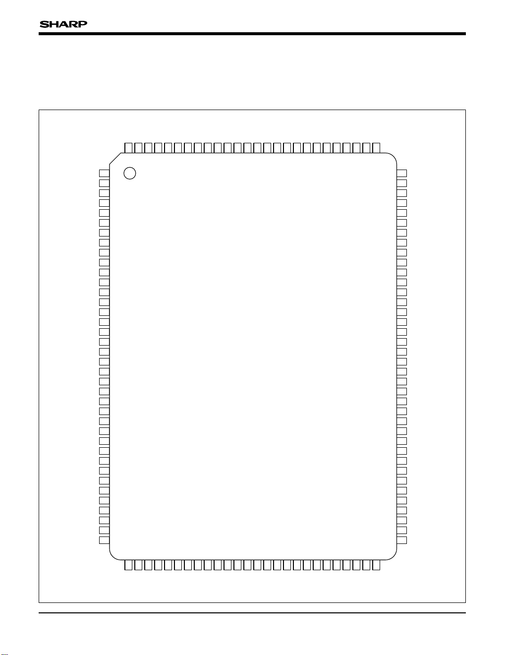
• Packages : 128-pin QFP (QFP128-P-1420)
SM8521
- 3 -
1
2
3
4
5
6
7
8
9
10
11
12
13
14
15
16
17
18
19
20
21
22
23
24
25
26
27
28
29
30
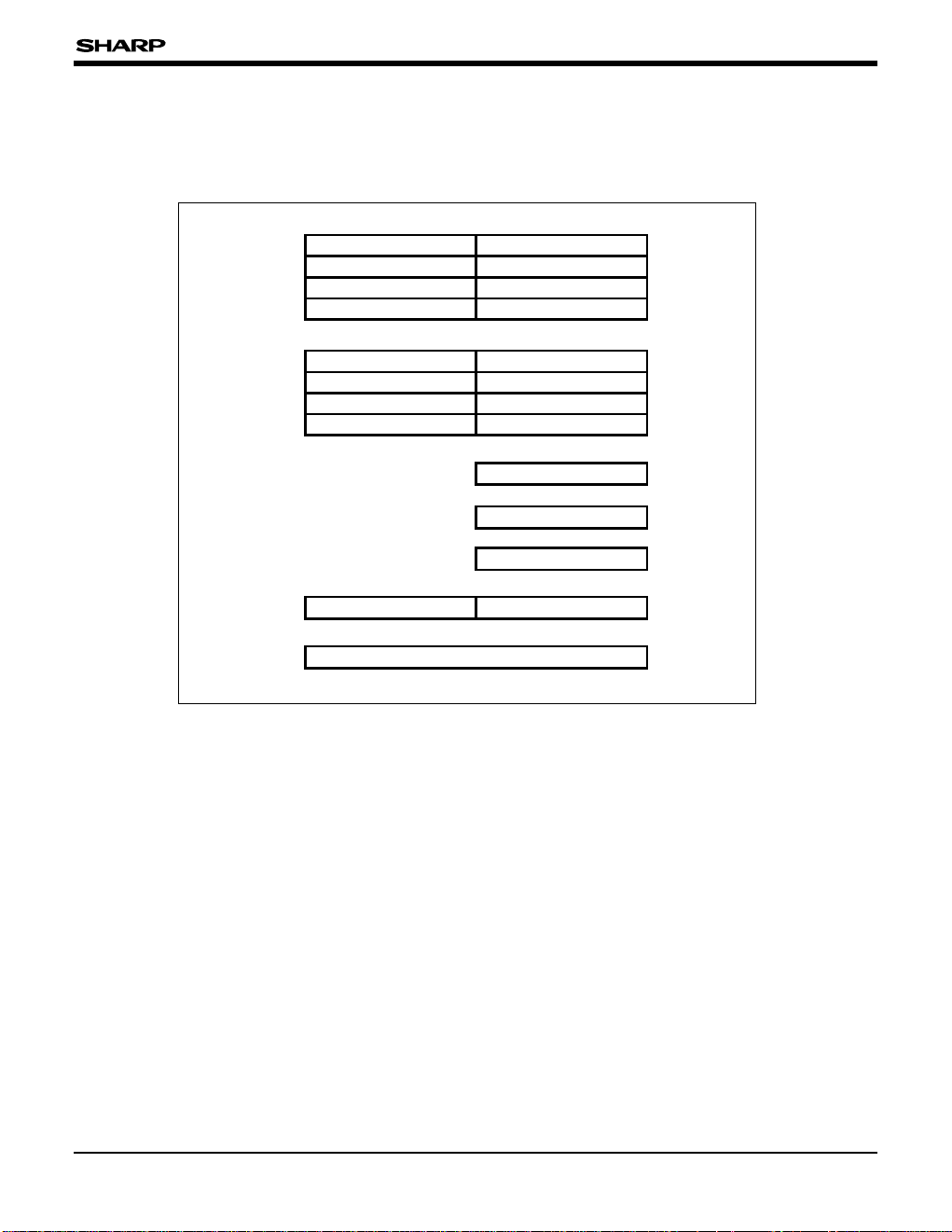
NC
D7
D6
D5
D4
D3
D2
D1
D0
A0
A1
A2
A3
A4
A5
A6
A7
A8
A9
A10
A11
A12
A13
A14
A15
A16
A17
A18
A19
A20
31RDB
32WRB
33MCE0B
34MCE1B
35IOE0B
36IOE1B
37GND
38GND
102
101
100
99
98
97
96
95
94
93
92
91
90
89
88
87
86
85
84
83
82
81
80
79
78
77
76
75
74
73
VD1
NC
NC
VD2
VD3
VD4
VD5
VD6
VD7
VCE0B
VCE1B
VRDB
VWRB
P3
7
P36
P35
P34
P33
P32
P31
P30
P27
P26
P25
P24
P23
P22
P21
P20
72 P16
P17
71 P15
70 P14
69 P13
68 P12
67 P11
66 NC
65 NC
39404142434445464748495051525354555657
58
GND
OSC1
OSC2
NC
INTB
NMIB
RESETB
M0M1M2
V
DD
RXDB
T
XDB
P0
0
P01
P02
P03
P04
P05
P06
59P07
60X1
61X2
62GND
63CLK
64P10
128
127
126
125
124
123
122
121
120
119
118
117
116
115
114
113
112
111
110
109
GNDVRSOUND
DOFFBFRLPXCXD0
XD1
XD2
XD3YDVA12
VA11
VA10
VA9
VA8
VA7
VA6
VA5
108
VA4
107
VA3
106
VA2
105
VA1
104
VA0
103
VD0
PIN CONNECTIONS
128-PIN QFP TOP VIEW
Page 4
SM8521
- 4 -
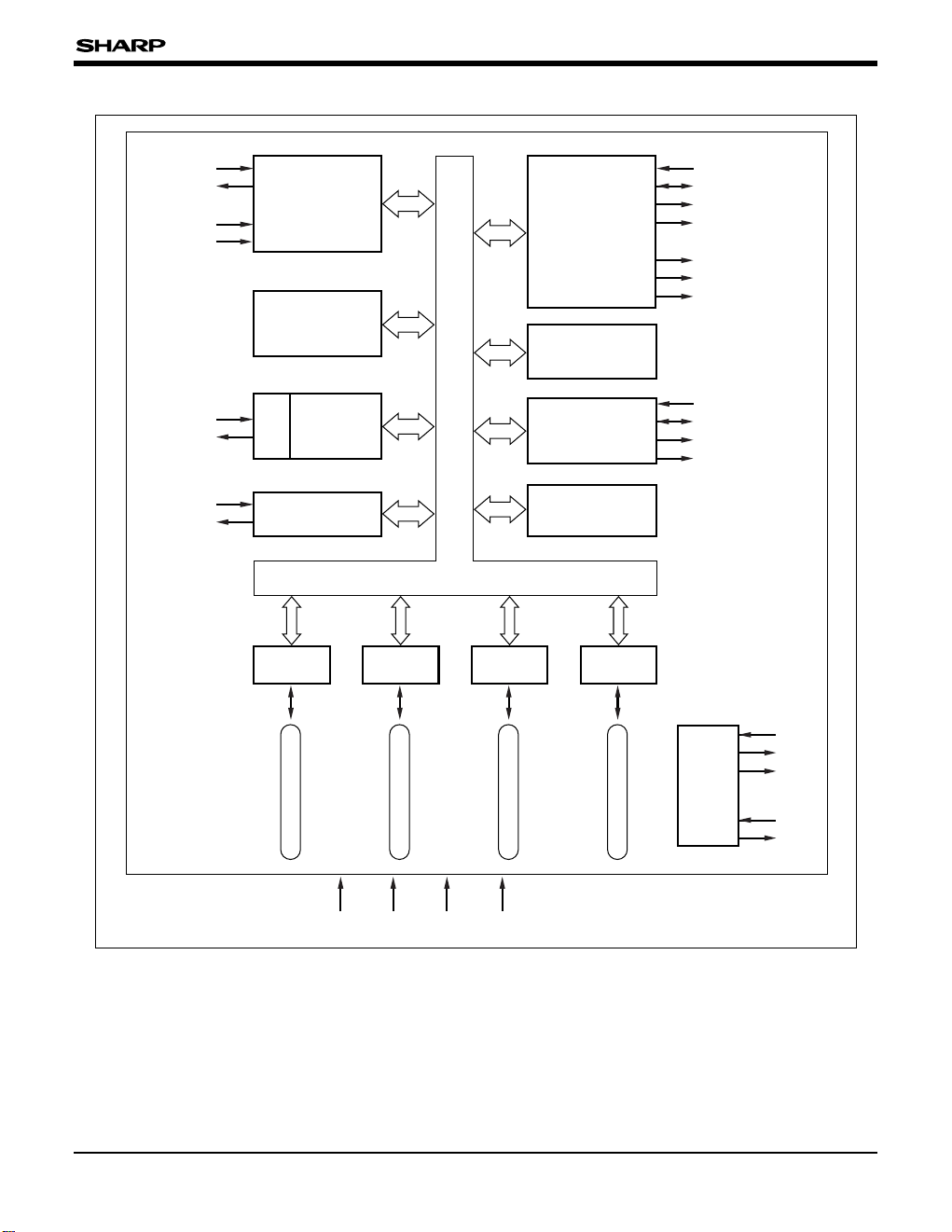
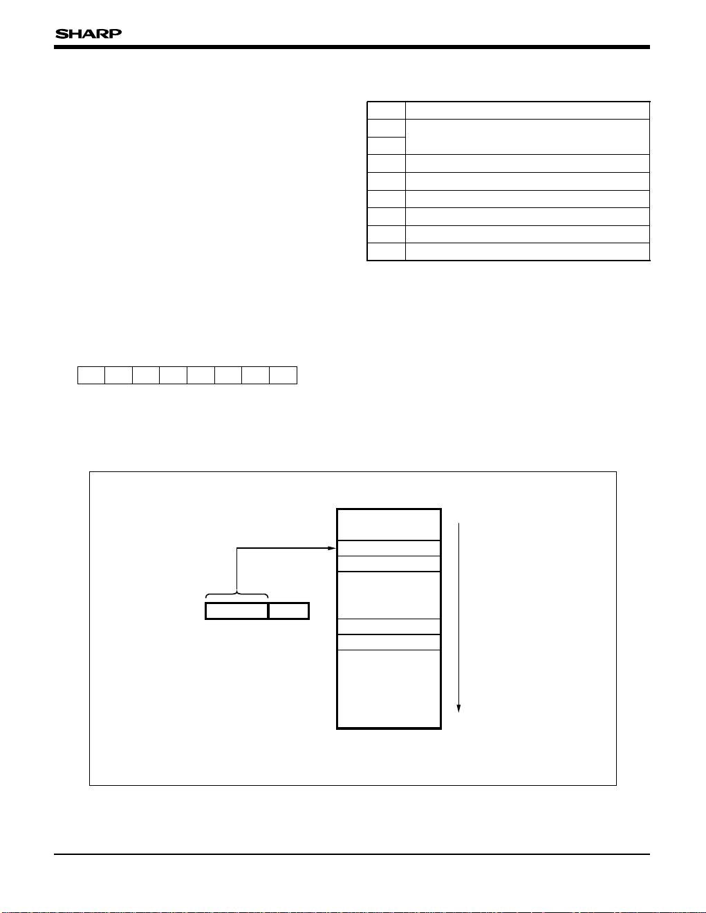
BLOCK DIAGRAM
RDB
WRB
VA0-VA12
VD0-VD7
INTB
NMIB
SM85CPU
RAM
1 k-BYTE
UART
P0
LCDC/DMA
RAM
4 k-BYTE
MMU
BUS CONTROLLER
TIMER 8-BIT : 2 CH
CLOCK
WATCHDOG TIMER
SOUND
GENERATOR
OSC
VRDB, VWRB
VCE0B, VCE1B
XD0-XD3
FR, LP, XC
YD, DOFFB
X2
X1
CLK
A0-A20
D0-D7
MCE0B, MCE1B
IOE0B, IOE1B
OSC2
OSC1
VR
SOUND
RXDB
TXDB
P00
P01
P02
P03
P04
P05
P06
P07
P10
P11
P12
P13
P14
P15
P16
P17
P20
P21
P22
P23
P24
P25
P26
P27
P30
P31
P32
P33
P34
P35
P36
P37
D/A
P1 P2 P3
GNDVDD RESETB M0-2
Page 5
- 5 -
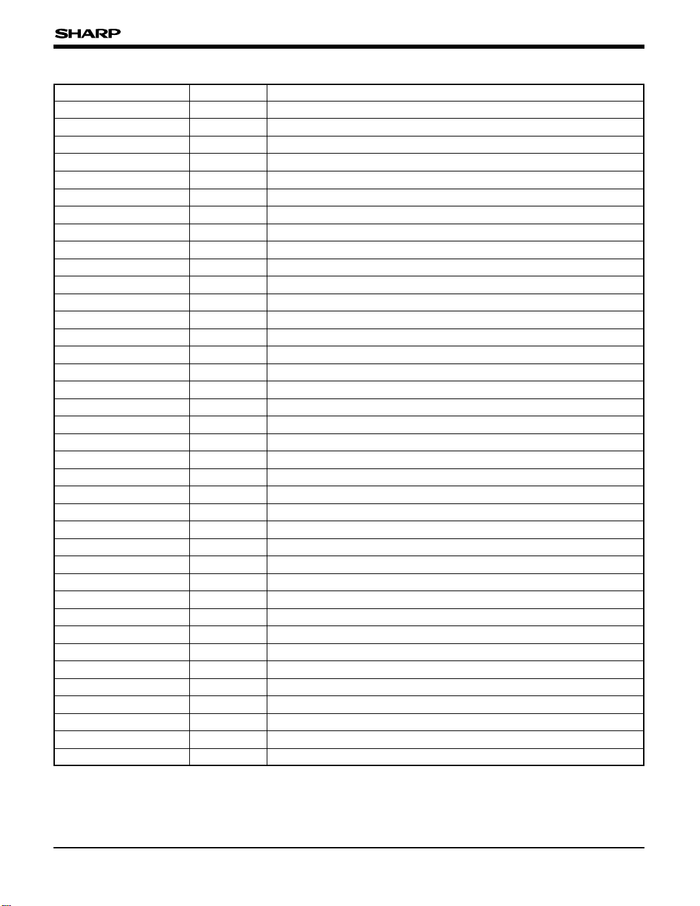
SM8521
PIN NAME I/O FUNCTION
D0-D7 I/O External data bus
A0-A20 O External address bus
MCE0B O Chip enable 0 (Mask ROM/flash memory)
MCE1B O Chip enable 1 (SRAM)
IOE0B O I/O enable 0 (address : FF00-FFFF)
IOE1B O I/O enable 1 (address : FF00-FFFF)
RDB O Read strobe
WRB O Write strobe
NMIB I Non-maskable interrupt
INTB I External interrupt
VD0-7 I/O VRAM data bus
VA0-12 O VRAM address bus
VCE0B O VRAM chip enable 0 (A000-BFFF)
VCE1B O VRAM chip enable 1(C000-DFFF)
VRDB O VRAM read strobe
VWRB O VRAM write strobe
P00-P07 I/O I/O port 0
P10-P17 I/O I/O port 1
P20-P27 I/O I/O port 2
P30-P37 I/O I/O port 3
RxDB I UART data input port
TxDB O UART data output port
SOUND O Sound output
VR I D/A converter reference voltage
FR O LCD drive waveform
LP O Display data latch pulse
XC O Display data clock
XD0-XD3 O Diaplay data
YD O Vertical timing
DOFFB O Display off
X1 I Main clock input
X2 O Main clock output
CLK O System clock output
OSC1 I Subclock input
OSC2 O Subclock output
RESETB I Reset
M0-M2 I Operation Mode (usually GND)
VCC, GND I Power supply
PIN DESCRIPTION
Page 6
SM8521
- 6 -
ABSOLUTE MAXIMUM RATINGS
PARAMETER SYMBOL CONDITION RATING UNIT
Supply voltage VDD – 0.3 to 6.5 V
Input voltage VI – 0.3 to VDD + 0.5 V
Output voltage VO – 0.3 to VDD + 0.5 V
Output current
IOH High-level output current 4 mA
IOL Low-level output current 4 mA
Operating temperature TOPR –10 to +60 ˚C
Store temperature TSTG –40 to +140 ˚C
RECOMMENDED OPERATING CONDITIONS
PARAMETER SYMBOL CONDITION RATING UNIT
Supply voltage VDD 4.5 to 5.5 V
System clock frequency fSYS VDD = 4.5 to 5.5 V 16.384 k to 5 M Hz
Maximum main clock frequency
fCK
VDD = 4.5 to 5.5 V 10 MHz
Subclock frequency fSUB VDD = 2.7 to 5.5 V 32.768 kHz
Operating temperature TOPR –10 to +60 ˚C
NOTE :
Be sure to RESETB when power on because internal signal reguires initialization. Normal operation is not guaranteed without
hardware reset.
Page 7
- 7 -
SM8521
NOTES :
1. Applicable pins : P00-P07, P10-P17, P20-P27, P30-P37, D0D7, VD0-VD7, X1, M0-M2
2. Applicable pins : RESETB, OSC1, RxDB, NMIB, INTB
3. Applicable pins : P0
0-P07, P10-P17, P20-P27, P30-P37,
VD0-VD7, X1, M0-M2 (non-connected
pull-up resistor)
4. Applicable pins : RESETB, P0
0-P07, P10-P17, P20-P27,
P3
0-P37 (connected pull-resistor)
5. Applicable pins : P0
0-P07, P10-P17, P20-P27, P30-P37, D0-
D7, A0-A20, MCE0B, MCE1B, IOE0B,
IOE1B, RDB, WRB, VA0-VA12, VCE0B,
VCE1B, VWRB, TxDB, XC, LP, FR,
CLK, XD0-XD3
6. No loadcondition, V
DD = 5 V, main clock = 10 MHz
7. No load condition, V
DD = 5 V, sub clock in active (32.768
kHz), VR = GND, input signal fixation.
8. No load condition, V
DD = 5 V, sub clock in active (32.768
kHz), VR = GND, input signal fixation.
Including LCD, DMA, sound generator and any part
concerned with timer operation.
9. No load condition, V
DD = 5 V, sub clock in active (32.768
kHz), VR = GND, input signal fixation.
10. No load condition, V
DD = 5 V, OSC1 = GND, VR = GND,
input signal fixation.
DC CHARACTERISTICS
PARAMETER SYMBOL
UNIT
NOTE
Input voltage
V
IH1 0.8 x VDD VDD
V 1
V
IH2 VDD – 0.5
0.5
10
V 2
VIL2
IIH1
µA
µA
3
4
IIL1 –10
IIL2 –40 –75 –150
0.5
8
10
± 0.10
45
18
70
6
± 0.05
30
15
30
1
Output voltage
VOH1 VDD – 0.5
V
bits
kΩ
V
mA
7
8
9
10
µA
µA
5
6
VOL1
D/A
Supply current
IDD
IDDH
IDDS1
IDDS2
MIN.
VIN = VDD, VDD = 5 V
VIH = 0 V, VDD = 5 V
VIN = 0 V, VDD = 5 V
IOH1 = –1 mA, VDD = 5 V
IOL1 = 10 mA, VDD = 5 V
VR = VDD = 5 V
VR = VDD = 5 V
VR = VDD = 5 V
fSYS = 5 MHz
fSYS = 5 MHz, HALT mode
fSUB oscillation, STOP mode
fSUB stop, STOP mode
MAX.TYP.
VIL1 0 0.2 x VDD
Input current
Resolution
Combined tolerance
Output resistance
(VDD = 4.5 to 5.5 V, TOPR = –10 to +60˚C)
CONDITION
Page 8
- 8 -
SM8521
SM85CPU
The SM85CPU is an 8-bit CPU with an unique
architecture, developed by SHARP, and the
following features.
General purpose register architectures
• There are eight 8-bit general purpose registers
(also serve as four 16-bit general purpose
registers) and four 16-bit general purpose
registers serve as accumulator, index register, or
the pointer registers.
General purpose register allocated at RAM
• The general purpose registers access the RAM
location by the register pointer RP. So pushing
the register during an interrupt and passing
parameter to subroutine can be executed in High
speed.
Refined instruction set
• The instruction set contains total 67 members : 8
load instructions, 19 arithmetic instructions, 7 logic
instructions, 9 program control (branch) instruction,
8 bit manipulation instructions, 8 rotate & shift
instructions and 9 CPU control instructions.
• There are powerful bit manipulation instructions
includes plural bits transfer, logical operation
between bits, and the bit test and jump instructions
that incorporates a test and condition branch in the
same instruction. (Refer to Table 1)
• There are data transfer, arithmetic and conditional
branch instructions for 16-bit. It can rapidly
process the word-sized and long jump.
• There are 8-bit x 8-bit
→16-bit multiplication and
16-bit x 16-bit→16-bit remaining 8-bit division
instructions. (Unsigned arithmetic)
23 address modes
• The rich address modes provides optimal access
to ROM, RAM and the register files.
Illegal instruction detecting function
• When an error code is detected, a non-maskable
interrupt (NMI) will be generated.
Standby function
• There are two standby modes, HALT and STOP
mode, and the mode can be changed by HALT
instruction or STOP instruction respectively.
Table 1 Instruction summary
TYPE INSTRUCTION NUMBER
Load instruction CLR, MOV, MOVM, MOVW, POP, POPW, PUSH, PUSHW 8
Arithmetic instruction
ADC, ADCW, ADD, ADDW, CMP, CMPW, DA, DEC, DECW, DIV,
EXTS, INC, INCW, MULT, NEG, SBC, SBCW, SUB, SUBW
19
Logic instruction AND, ANDW, COM, OR, ORW, XOR, XORW 7
Program control instruction BBC, BBS, BR, CALL, CALS, DBNZ, IRET, JMP, RET 9
Bit manipulation instruction BAND, BCLR, BCMP, BMOV, BOR, BTST, BSET, BXOR 8
Rotate & shift instruction RL, RLC, RR, RRC, SLL, SRA, SRL, SWAP 8
CPU control instruction COMC, CLRC, DI, EI, HALT, NOP, SETC, STOP 8
Total 67
Page 9
SM8521
- 9 -
Table 2 Addressing Mode Summary
NAME SYMBOL Range
Operand
∗
1
Implied
To specify the carry(C) and interrupt enable
(I) in the instruction code.
Register r r = R0-R7 General register [byte]
Register pair rr r = RR0, RR2, … , RR14 General register [word]
Register file R R = 0 to 255 (R0-R15)
Register file (0000H-007FH) and (0080H-00FFH)
[byte]
Register file pair RR
R = 0, 2, … 254
(RR0, RR2, … , RR14)
Register file (0000H-007FH) and (0080H-00FFH)
[byte]
Register indirect @r r = R0-R7 Memory (0000H-00FFH) [byte]
Register indirect
auto increment
(r)+ r = R0-R7 Memory (0000H-00FFH) [byte]
Register indirect
auto decrement
–(r) r = R0-R7 Memory (0000H-00FFH) [byte]
Register index
n(r)
∗
2
n = 00H-FFH, r = R1-R7 Memory (0000H-00FFH) [byte]
Register pair indirect @rr rr = RR0, RR2, … , RR14 Memory (0000H-FFFFH) [word/byte]
Register pair indirect
auto increment
(rr)+ rr = RR0, RR2, … , RR14 Memory (0000H-FFFFH) [word/byte]
Register pair indirect
auto decrement
–(rr) rr = RR0, RR2, … , RR14 Memory (0000H-FFFFH) [word/byte]
Register pair index
nn(rr)
∗
3
nn = 0000H-FFFFH
rr = RR2, RR4, … , RR14
Memory (0000H-FFFFH) [word/byte]
Index indirect
@nn(r)
∗
2
nn = 0000H-FFFFH
r = R1-R7
Memory (0000H-FFFFH) [word]
Immediate IM IM = 00H-FFH
The immediate data in the instruction code [byte]
Immediate long IML IML = 0000H-FFFFH
The immediate data in the instruction code [word]
Bit b b = 0 to 7
Register file (0000H-007FH) and memory
(0080H-00FFH, FF00H-FFFFH) [bit] (1bit of 1 byte
pointed by R, n(r) and DAp)
Port p Register file (0010H-0017H) [byte]
Relative RA PC – 128 to PC + 127 Program memory (1000H-FFFFH)
Direct DA DA = 0000H-FFFFH Memory (0000H-FFFFH) [byte]
Direct short DAs DAs = 1000H-1FFFH Program memory (1000H-1FFFH)
Direct special page DAp DAp = FF00H-FFFFH Program memory (FF00H-FFFFH) [byte]
Direct indirect @DA
DA = 0000H-FFFFH
Memory (0000H-FFFFH)
∗
1 The data indicated by [ ] is the unit of possible to use in Load and Arithmetic Instructions.
∗
2 R0 can not be used.
∗
3 RR0 can not be used.
Page 10
SM8521
- 10 -
Register Lineup
Fig. 1 shows the SM85CPU register lineup. The CPU
internal register consists of eight 8-bit general purpose
registers (R0-R7), four 16-bit general purpose registers
(RR8-RR14), a program counter (PC) and four other
control registers. (The R0-R7 can be also used as
four 16-bit general purpose registers (RR8-RR14).)
GENERAL PURPOSE REGISTER
The eight 8-bit
general purpose registers
R0-R7 and
all eight 16-bit general purpose registers (RR0RR14) are available for use as accumulator, index
register and pointer registers. (The R0 and RR0
cannot be used as index register)
The other eight 8-bit registers R8-R15 cannot be used
as 8-bit general purpose register and as member of
the register file. (about register file, refer to "Address
Space.")
The feature of the SM85CPU architecture is that
general purpose registers
are virtually allocated at
16-byte internal RAM. Actually, if the CPU accesses
general purpose registers
, the designated RAM will
be accessed by the 5-bit register pointer (RP)
✽
.
When RP = 00000B, the registers occupy the first
16 bytes starting at 0000
H. Incrementing the field,
RP = 00001B, shifts the mapping by eight bytes so
that the registers start at 0008
H. As a result, the
general purpose registers
can be switched in 8-byte
unit to any RAM location within 0000
H-00FFH.
Although the
general purpose registers
are members
of the register file, which stores the data onto
actual RAM, is different from the other members
(control registers).
That is, general purpose registers can be referred as
registers, as register file (allocated at 0000
H
-000FH)
and as RAM accessing by all addressing modes.
∗ About register pointer (RP), refer to "Processor status 0
(PS0)".
RR0
RR2
RR4
RR6
R8
R10
R12
R14
RR8
RR10
RR12
RR14
R0
R2
R4
R6
7
15
07 0
R1
R3
R5
R7
R9
R11
R13
R15
0
70
70
70
7070
0
15
PS0
PS1
SYS
SPLSPH
PC
Fig. 1 Register Lineup
Page 11
SM8521
- 11 -
CPU CONTROL REGISTER
The SM85CPU has the following control register :
processor status PS0, processor status PS1,
system configuration register SYS, stack pointer
SPH, SPL and program counter PC. All control
register except the program counter PC are
members of the register file and accessible by the
register file R and the register file pair RR
addressing modes.
Processor status 0 (PS0)
The processor status PS0 is an 8-bit readable/
writable register containing 2 fields, the upper 5-bit
is register pointer (RP) and the lower 3-bit is
interrupt mask.
Bit 7 0
Bits 7 to 3 : Register pointer (RP)
This gives, in 8 bytes unit, the starting address
in RAM for
general purpose registers
.
Bits 2 to 0 : Interrupt mask bits (IM)
Internal RAM
Address
R0
R1
R14
R15
High
Low
RP IMPS0
Ex.)
If RP=00000B, general purpose
registers will be virtually allocated
at internal RAM 0000H-000FH.
If RP=00001B, general purpose
registers will be virtually allocated
at internal RAM 0008H-0017H.
Fig. 2 Register Pointer (RP) Setting Example
BIT CONTENT
000
All maskable interrupts recognized
001
010
Maskable interrupts with level 1 to 12 recognized
011
Maskable interrupts with level 1 to 10 recognized
100
Maskable interrupts with level 1 to 8 recognized
101
Maskable interrupts with level 1 to 6 recognized
111
Maskable interrupts with level 1 tto 4 recognized
111
Maskable interrupts with level 1 to 2 recognized
PR4 PR3 PR2 PR1 PR0 IM2 IM1 IM0
Page 12
- 12 -
SM8521
Processor status 1 (PS1)
The processor status PS1 is an 8-bit readable/
writable register and consists of eight flag bits.
These flags can be used as the condition codes for
the conditional branch instructions. When CPU
generates an interrupt, the content of processor
status PS1 and the value of program counter PC
automatically are pushed onto stack.
Bit 7 0
Bit 7 : Carry (C)
It indicates that generated a carry in operation.
Bit 6 : Zero (Z)
It indicates that the operation result is zero.
Bit 5 : Sign (S)
It indicates that the operation result is negative
(Sign bit = ‘1’).
Bit 4 : Overflow (V)
Executes the operation with the signed value. If
the operation result cannot indicate complement
on two, then the bit will be ‘1’.
Bit 3 : Decimal adjustment (D)
It indicates that the last arithmetic operation is a
subtraction.
Bit 2 : Half carry (H)
It indicates that generated a carry between bit 3
and 4.
Bit 1 : Bit (B)
It indicates that the result of the last bit
manipulation.
Bit 0 : Interrupt enable (I)
This is a flag which enables/disables all
maskable interrupt.
System configuration register (SYS)
The system configuration register SYS is an 8-bit
readable/writable register which sets the external
memory expansion modes and selects 8-bit/16-bit
stack pointer.
Bit 7 0
Bit 7 : Sets '0'
Bit 6 : Stack pointer configuration (SPC)
Bits 5 to 3 : Set '0'
Bits 2 to 0 : Memory configuration (MCNF2-0)
∗ : In ROM space (60 k bytes), the field beyond the internal
ROM is the external memory access field.
Stack pointer (SPL, SPH)
The stack pointer SPL, SPH are 8-bit readable/
writable register and show the stack address. The
bit SPC of the system configuration (SYS) specifies
whether the stack pointer is 8 (SPL only) or 16
(both SPL and SPH) bits long.
Program counter (PC)
The program counter (PC) is a pointer for program
memory and contains the starting address for the
next instruction.
The program counter PC is initialized to 1020
H after
hardware reset. That is, the application program
starts executing from the address 1020
H after
hardware reset.
0
BIT
8-bit (SPL only)
CONTENT
1 16-bit (both SPL, SPH)
- SPC - - -
MCNF2 MCNF1 MCNF0
CZSVDHBI
BIT CONTENT
000 External memory expansion disable.
110
External memory expansion mode
(64 k bytes✽)
Other
combination
Do not use.
Bit 15 0
Page 13
SM8521
- 13 -
76543210
MSB LSB
MSB
Upper 8-bit
LSB
Lower 8-bit
Address
High
Low
Data Format
0000
H-00FFH
0000H-00FFH
Even byte, 0000H-00FEH,
following byte (odd byte)
0000H-00FFH
Register file address
Bit
Byte
Word
BCD
Data
Type
70
Upper BCD digit Lower BCD digit
0000H-00FFH or FF00H-FFFFH
0000H-00FFH
0000H-00FFH or FF00H-FFFFH
(Under shorthand)
0000
H-FFFEH
following byte
0000
H-00FFH
Memory address
Fig. 3 Register File/Memory Data Formats
Address Space
The SM85CPU has a 64 k-byte address space,
which is divided into RAM (0000
H-0FFFH) and ROM
(1000
H-FFFFH) areas. The address 0000H-007FH
are both shared by RAM and register file. Fig. 9-1
shows the SM8521 Memory Map.
The RAM and register file allocated at 0000
H-007FH
can be selected by the addressing mode
designated by instructions.
The SM8521 supports an Memory Management
Unit used to external memory area expantion.
Refer to "Memory Management Unit (MMU)".
ROM Area
ROM area starts at the address 1000H of the space
address. The first portion (1000
H-101FH) is reserved
for the interrupt vector table. Each 2 bytes entry in
the vector table contains the address of interrupts.
When an interrupt encountered, the CPU jumps to
the corresponding branch address of vector table
for program executing. The address 1020
H marks
the start of the user program area itself. Executing
always starts at 1020
H after hardware reset.
Register File Area
The register file is allocated between 0000H and
007F
H. The first 16 bytes (0000H-000FH) area are
general registers. The remainder is for CPU control
registers, peripherals control register and data
register.
RAM Area
The RAM area starts at the beginning 0000H of the
address space. It overlaps the register file for the
address 0000
H-007FH.
This arrangement is to shorten the instruction
length as much as possible and to permit the use
with both RAM and the register file for faster
execution.
Page 14

- 14 -
SM8521
Data Format
The SM85CPU supports four data types : bit, 4-bit
BCD, byte, and word data.
REGISTER FILE DATA FORMATS
The register file (0000H-007FH) and RAM (0080H-
00FF
H) accessible with register file R and register
file pair RR addressing support processing for all 4
data types : bit, 4-bit BCD, byte, and word data.
Fig. 3 shows the data layout in the register file.
• Bit data (register file)
Bit manipulation instructions access bit data in the
register by register file R addressing, which gives
the byte address in the register file (0000
H-007FH),
or RAM (0080
H-00FFH), and the operand b, which
gives the bit number within the byte.
• Byte data (register file)
Instructions access the byte data in the register file
by register file R addressing, which gives the byte
data address in the register file (0000
H-007FH) or
RAM (0080
H-00FFH).
• Word data (register file)
Instructions access word data in the register file by
register file pair RR addressing, which gives the word
address, even and 2 bytes address, in the register
file (0000
H-007FH) or RAM (0080H-00FFH). The
address must be even (0, 2, 4,…, 254). Specifying an
odd address leads to unreliable results.
• BCD data (register file)
The decimal adjust instruction (DA), used to adjust
BCD digits after an odd or subtraction, accesses a
BCD data byte in the register file by register file R
addressing.
•
Notice for the general register on register file
The general registers are the first 16 bytes (0000H-
000F
H) in the register file. They can be accessed
as byte-sized by register file R addressing and as
word-sized by register file pair RR addressing.
MEMORY DATA FORMATS
The memory area (ROM and RAM 0000H-FFFFH)
supports processing for all 4 data types : bit, 4-bit
BCD, byte and word data. However, bit data is
limited to the ranges (0000
H-00FFH, FF00H-FFFFH),
and 4-bit BCD data to the ranges 0000
H-00FFH.
Fig. 3 shows the data layout in memory.
• Bit data (memory)
Bit manipulation instructions access bit data in
memory by register index n(r) addressing, which
gives the byte address in the range (0000
H-00FFH),
or by direct special page DAp addressing, which
gives the byte address in the range (FF00
H-FFFFH),
and the operand b, which gives the bit number
within the byte.
• Byte data (memory)
Instructions access the byte data in memory by
shorthand (0000
H-00FFH or FF00H-FFFFH) or full
(0000
H-FFFFH) address.
• Word data (memory)
Instructions access the word data, continue 2
bytes, in memory by shorthand (0000
H-00FFH or
FF00
H-FFFFH) or full (0000H-FFFFH) address.
Unlike word data in the register file, the address
can be even or odd.
• BCD data (memory)
The decimal adjust instruction (DA), used to adjust
BCD digits after an odd or subtraction, accesses a
BCD data byte in memory by register index @r
addressing.
• Notice for general register on memory
The general registers are actually in a RAM area
specified by register pointer RP, so they can be
read and modify directly as RAM. While
programming, the programmer must take care to
arrange program data so that other RAM
operations do not destroy general registers content.
Page 15
SM8521
- 15 -
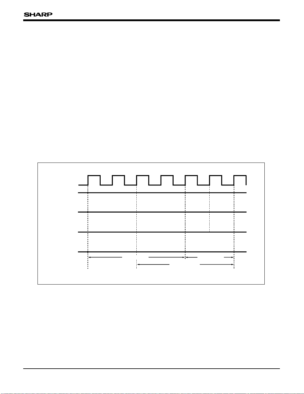
Bus Timing
The SM85CPU is variable for system clock. The bit
FCPUS2-FCPUS0 (bits 5 to 3 : CKKC) of the clock
changing register CKKC can select system clock to
1/2, 1/4, 1/8, 1/16 and 1/32 of the main clock and
1/2 of sub-clock. The CPU operates at 1/32 clock
of the main clock after hardware reset.
INTERNAL MEMORY ACCESS TIMING
The read cycle of internal RAM is 2 cycles. The
internal RAM supports 2 cycles for reading or
writing.
EXTERNAL MEMORY ACCESS TIMING
The external memory supports 2 cycles for reading
or writing. Fig. 5 shows the read timing and Fig. 6
shows the write timing.
INSTRUCTION PREFETCH
The SM85CPU, which execution cycle overlaps
with the OP code, fetches next instruction OP
code during one instruction execution cycle. For
example, the execution time for 2 bytes instructions
(MOV R, r) of transferring the RAM contents to a
register is 4 cycles.
Internal clock
Pre-instruction
Transfer
instruction
Next instruction
Fetch cycle
Execution
cycle
Executing
preinstruction
OP code
fetch
Operand
fetch
RAM
read
Register
write
OP code
fetch
Execution time
Fig. 4 Instruction Execution for Transfer Instruction (2 Bytes)
Page 16
SM8521
- 16 -
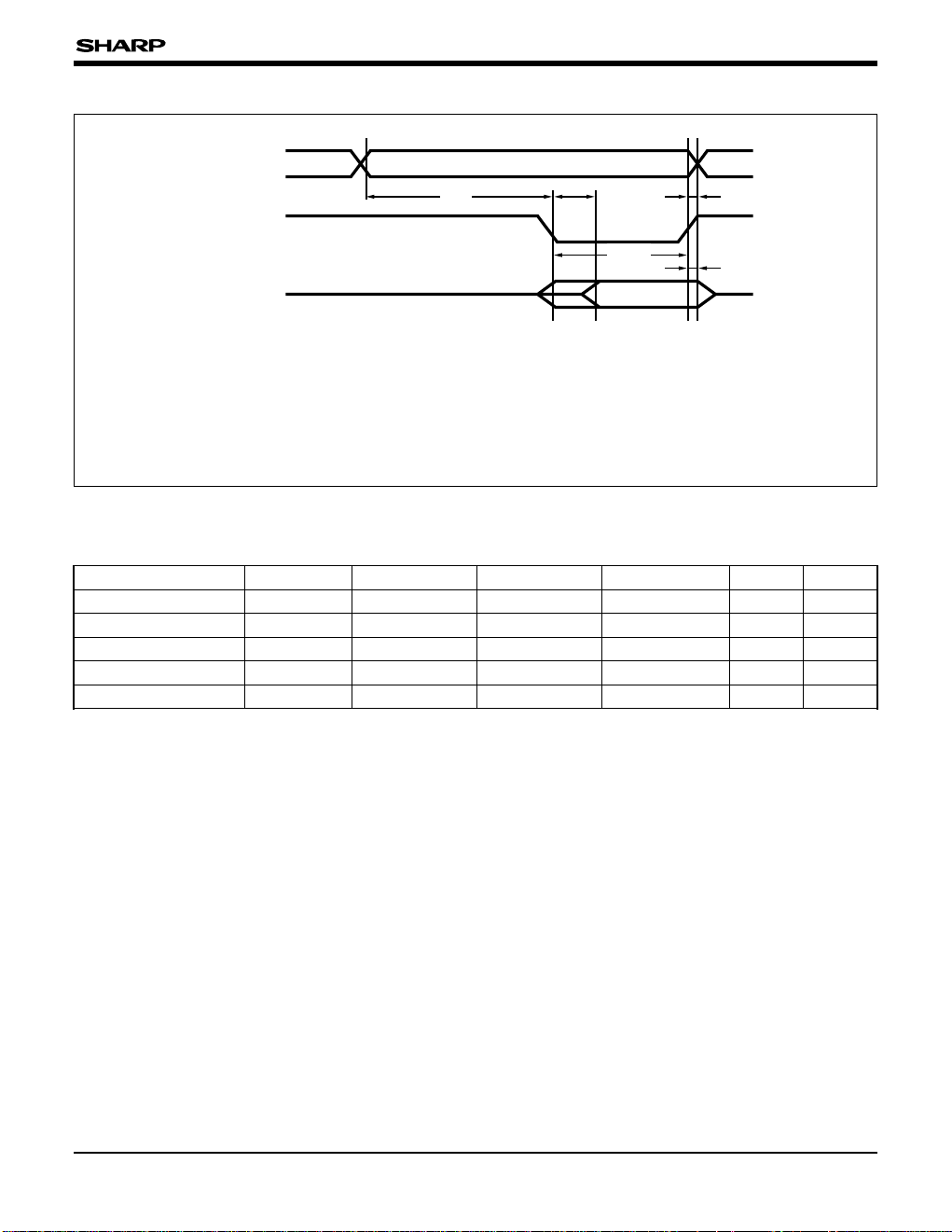
RDB
Valid data
D0-D7
t
RHD
t
RHA
t
RSA
t
RSD
t
WRD
A0-A
20
• External memory access timing (read timing)
Operating condition (VDD = 4.5 to 5.5 V, TOPR = –10 to 60˚C)
PARAMETER SYMBOL UNIT
NOTE
Address setup time tRSA tSYS tSYS + 50 ns 1
Read data setup time tRSD tSYS/2 – 30 ns 1
RDB signal pulse width
tWRD tSYS – 50 tSYS ns 1
Address hold time tRHA 0 ns
Read data hold time tRHD 0 ns
MIN. TYP. MAX.
NOTE :
1. tSYS : The system clock period (main clock x 1/2) when the
low order 3 bits in the clock change register
FCPUS2-FCPUS0 are 100
B.
tRSA : The time between address firm and RDB signal
falling Low level firm.
t
RSD : The time between RDB signal firm and input valid
data firm.
t
WRD : RDB signal Low level width.
t
RHA : The time between RDB signal rising High level firm
and address change.
t
RHD : The time between RDB signal rising High level firm
and output data floating.
Load capacitance is 50 pF.
Fig. 5 External Memory Access Timing (Read Timing)
Page 17
SM8521
- 17 -
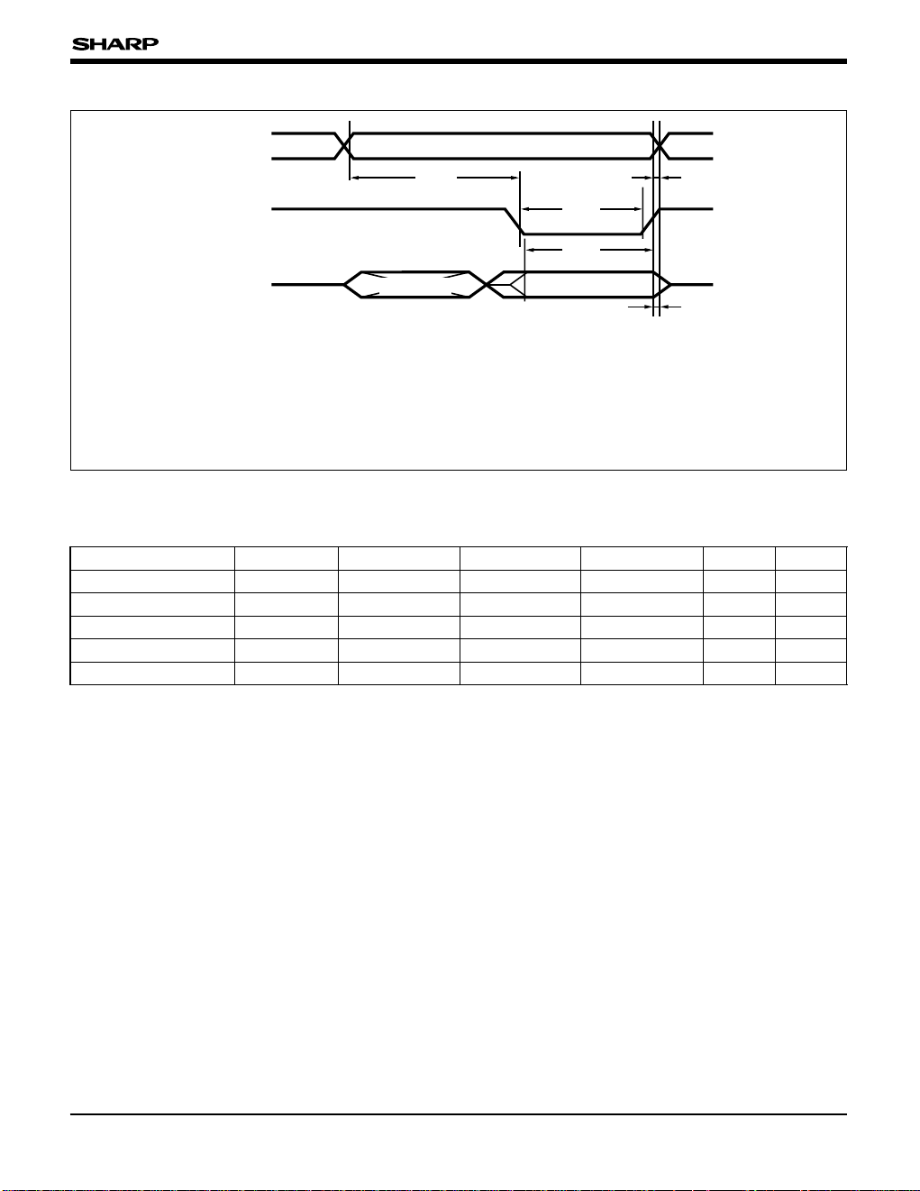
WRB
D
0
-D7
Valid data
t
WSA
Invalid data
t
WSD
t
WHD
t
WHA
t
WWR
A0-A
20
• External memory access timing (write timing)
Operating condition (VDD = 4.5 to 5.5 V, TOPR = –10 to 60˚C)
PARAMETER SYMBOL UNIT NOTE
Address setup time tWSA
tSYS
tSYS + 50
ns
1
Data setup time tWSD tSYS – 50 tSYS + 30
ns
1
WRB signal pulse width
tWWR tSYS – 60
tSYS ns
1
Address hold time tWHA 10
ns
Data hold time tWHD 10
ns
MIN. TYP. MAX.
NOTE :
1. tSYS : The system clock period (main clock x 1/2) when the
low order 3 bits in the clock change register
FCPUS2-FCPUS0 are 100
B.
t
WSA : The time between address firm and WRB signal
falling Low level firm.
t
WSD : The time between WRB signal rising High level firm
and output valid data firm.
t
WWR : WRB signal Low level width.
t
WHA : The time between WRB signal rising High level firm
and address change.
t
WHD : The time between WRB signal rising High level firm
and output data floating.
Load capacitance is 50 pF.
Fig. 6 External Memory Access Timing (Write Timing)
Page 18

SM8521
- 18 -
SYSTEM CONTROL
Oscillator Circuit
The SM8521 is built-in the main-clock and subclock oscillator circuits for generating clock signal.
The main-clock oscillator circuit is applied to 1.5 to
10 MHz. The sub-clock oscillator circuit is applied
to 32.768 kHz.
Clock System
The SM8521 uses the main-clock and sub-clock
oscillator circuits to generate the required clock.
The system clock, leads CPU operation, is one of
the five clocks which divides the main-clock (f
CK)
into 1/2, 1/4, 1/8, 1/16 and 1/32. It also selects
from sub-clock (f
32K). In addition, the clocks
supplied to the peripheral functions are fc
1-fc10
divided by the prescaler PRS0 and derived from
the 1/2 clock of main-clock (f
CK/2), and fx1-fx8 divided
by the prescaler PRS1 and derived from the subclock.
fCK = 11.0592 MHz
System clock
frequency control
CG
SM85CPU
Warming up counter
Sub-clock
generator circuit
Prescaler PRS1
CKIN
CKOUT
OSCIN
OSCOUT
RAM register
read/write
Function blocks
operation
Peripheral functions
Interrupt control
fCK/2 f
c
1-fc10
f
c
10
System clock
f32K
f32K
f32K = 32.768 kHz
Main-clock
generator circuit
1/2
Prescaler PRS0
fCK
Fig. 7 SM8521 Clock System
Page 19

SM8521
- 19 -
Clock change register (CKKC)
Clock change register CKKC is an 8-bit readable/
writable register containing the control of system
clock change and the setting of warming up period
after waking up from the STOP mode.
Clock change register CKKC is initialized to 00
H
after hardware reset.
Bit 7 0
Bit 7 : Clock change enable bit (FCPUEN)
Bit 6 : Main-clock stopped bit (MCKSTP)
Main-clock stopped allows switching to sub-clock
used as system clock.
Bits 5 to 3 : System clock selection bits
(FCPUS2-FCPUS0)
Under the bit FCPUEN = ‘1’, if executes the
STOP instruction, the bits will be valid.
Bit 2 : Reserved bit (TFCPU)
Always write ‘0’ to this position. Writing a ‘1’
produces unrealiable operation.
Bits 1 to 0 : Warming up selection bits
(WUPS1-WUPS10)
The bits are able to set the warming up period
of after wake up from STOP mode.
BIT SYSTEM CLOCK FREQUENCY
000 System clock = (1/32) x main-clock
001 System clock = (1/16) x main-clock
010 System clock = (1/8) x main-clock
011 System clock = (1/4) x main-clock
101, 110 Reserved
100 System clock = (1/2) x main-clock
111 System clock = (1/2) x sub-clock
BIT
WARMING UP PERIOD AFTER STOP
MODE RELEASES
(when main-clock (f
CK) = 10 MHz)
00 218x main-clock period (26.21 ms)
01 217x main-clock period (13.10 ms)
10 216x main-clock period (6.553 ms)
11 215x main-clock period (3.276 ms)
FCPUEN MCKSTP FCPUS2 FCPUS1 FCPUS0 TFCPU WUPS1 WUPS0
Fig. 8 SM8521 Clock System (Equivalent Circuit for Clock System Peripheral Blocks)
fCK
Main-clock
1/2 1/2 1/2 1/2
1/2
1/2 1/2 1/2 1/2 1/2 1/2 1/2 1/2 1/2 1/2 1/2 1/2 1/2 1/2 1/2 1/2
CG
System clock fSYS
1/2 1/2 1/2 1/2 1/2 1/2 1/2 1/2
5
Selector
f32K
f32K
fCK/4 fCK/8 fCK/16 fCK/32
System clock frequency control
Prescaler PRS0 (frequency divider on fCK/2)
Prescaler PRS1 (frequency divider on f32K)
Sub-clock
f
c
10 fc11 fc12 fc13 fc14 fc15 fc16
f
x
1 fx2 fx3 fx4 fx5 fx6 fx7 fx8
8
fCK/2
f
CK/2
1/2 1/2
1/2
1/2 1/2 1/2 1/2
1/2 1/2 1/2 1/2 1/2
f
c
12 fc13 fc14 fc15
Prescaler PRS2 (frequency divider on fc10)
Warming up counter (frequency divider on fc10)
For warming
up counter
8
To function blocks
BIT CONTENT
0 Disables system clock speed change
1 Enables system clock speed change
BIT CONTENT
0 Main-clock operation
1 Main-clock stop
Page 20

SM8521
- 20 -
Memory Map
Fig.9 shows the SM8521 memory map.
RAM
physically
present
Area
ROM physically present Area
Register file
physically
present
Area
Reserved Area
External
ROM
External
ROM
External
ROM
External
ROM
External
ROM
Internal
ROM
Reserved area
Interrupt vector
area
∗3
VRAM
Extend I/O
Extend RAM
∗1 ∗2
0000
H
0080H
007FH
0400H
03FFH
1000H
0FFFH
1020H
101FH
2000H
1FFFH
4000H
3FFFH
6000H
5FFFH
8000H
7FFFH
A000H
9FFFH
E000H
DFFFH
FFFFH
∗1 ROM disable (In case of MMU0 is set.)
∗2 ROM enable (At reset)
∗3 Write only during CPU access
0000H
General register
General register
General register
Control register
System Configuration Register
Clock change register
Stack Pointer
Reserved
Stack Pointer
Processor Status 0
Processor Status 1
–
Control register
R0R1R15
SYS
CKC
SPH
SPL
PS0
PS1
0001
H
000FH
0010H
0018H
0019H
001AH
001BH
001CH
001DH
001EH
001FH
0020H
007FH
Address Space
Register File
Interrupt Vector
DMA
(DMA)
(Upper)
(Lower)
1000H
1001H
Timer 0
(TIM 0)
(Upper)
(Lower)
1002H
1003H
Reserved
(Upper)
(Lower)
1004H
1005H
External Interrupt
(EXTINT)
(Upper)
(Lower)
1006H
1007H
UART transmit/receive
completion (UART)
(Upper)
(Lower)
1008H
1009H
Reserved
Reserved
(Upper)
(Lower)
100AH
100BH
(Upper)
(Lower)
100CH
100DH
LCD controler
(LCDC)
(Upper)
(Lower)
100EH
100FH
Reserved
(Upper)
(Lower)
1010H
1011H
Timer 1
(TIM 1)
(Upper)
(Lower)
1012H
1013H
Reserved
(Upper)
(Lower)
1014H
1015H
Clock
(CK)
(Upper)
(Lower)
1016H
1017H
Reserved
(Upper)
(Lower)
1018H
1019H
Input/output port
(PIO)
(Upper)
(Lower)
101AH
101BH
Watchdog timer
(WDTINT)
(Upper)
(Lower)
(Upper)
(Lower)
101CH
101DH
NMI, illegal instrtuction
(NMI, ILL)
101EH
101FH
Fig. 9-1 SM8521 Memory Map (1)
Page 21

SM8521
- 21 -
Fig. 9-2 SM8521 Memory Map (2)
Address Register name R/W
Initial value
0000H
General purpose register
R0
RR0
R/W Undefined
0001
H
General purpose register
R1 R/W Undefined
0002
H
General purpose register
R2
RR2
R/W Undefined
0003
H
General purpose register
R3 R/W Undefined
0004
H
General purpose register
R4
RR4
R/W Undefined
0005
H
General purpose register
R5 R/W Undefined
0006
H
General purpose register
R6
RR6
R/W Undefined
0007
H
General purpose register
R7 R/W Undefined
0008
H
General purpose register
R8
RR8
R/W Undefined
0009
H
General purpose register
R9 R/W Undefined
000A
H
General purpose register
R10
RR10
R/W Undefined
000B
H
General purpose register
R11 R/W Undefined
000C
H
General purpose register
R12
RR12
R/W Undefined
000D
H
General purpose register
R13 R/W Undefined
000E
H
General purpose register
R14
RR14
R/W Undefined
000F
H
General purpose register
R15 R/W Undefined
0010
H Interrupt enable register 0 IE0 R/W 00H
0011H Interrupt enable register 1 IE1 R/W 00H
0012H Interrupt request register 0 IR0 R/W 00H
0013H Interrupt request register 1 IR1 R/W 00H
0014H PIO data register 0 P0 R/W 00H
0015H PIO data register 1 P1 R/W 00H
0016H PIO data register 2 P2 R/W 00H
0017H PIO data register 3 P3 R/W 00H
0018H Reserved - -
0019
H System configuration register SYS R/W
∗
0000000
001A
H Clock change register CKC R/W 00H
001BH Reserved - -
001C
H Stack pointer H SPH
SP
R/W Undefined
001D
H Stack pointer L SPL R/W Undefined
001E
H Processor status register 0 PS0 R/W Undefined
001F
H Processor status register 1 PS1 R/W
∗∗∗∗∗∗∗
0
Address Register name R/W
Initial value
0020H PIO control register 0 P0C R/W 00H
0021H PIO control register 1 P1C R/W 00H
0022H PIO control register 2 P2C R/W 00H
0023H PIO control register 3 P3C R/W 00H
0024H MMU data register 0 MMU0 R/W 00H
0025H MMU data register 1 MMU1 R/W 00H
0026H MMU data register 2 MMU2 R/W 00H
0027H MMU data register 3 MMU3 R/W 00H
0028H MMU data register 4 MMU4 R/W 00H
0029H Reseved - -
002A
H Reseved - -
002B
H UART Transmit data register URTT W FFH
002CH UART Receive data register URTR R 00H
002DH UART Status register URTS R 0
∗
000010
002E
H UART Control register URTC R/W 00H
002FH Reseved - -
0030
H Control/Status register LCC R/W 00H
0031H Display H-timing register LCH R/W ∗∗000000
0032
H Display V-timing register LCV R/W
*
1
0∗000000
0033
H Reserved - -
0034
H Controler register DMC R/W 0∗000000
0035
H
Source X-coordinate register
DMX-1 R/W 00H
0036H
Source Y-coordinate register
DMY-1 R/W 00H
0037H X-width register DMDX R/W 00H
0038H Y-width register DMDY R/W 00H
0039H
Destination X-coordinate register
DMX2 R/W 00H
003AH
Destination Y-coordinate register
DMY2 R/W 00H
003BH Pallet register DMPL R/W 00H
003CH ROM bank register DMBR R/W ∗0000000
003D
H VRAM page register DMVP R/W ∗∗∗∗∗∗00
003E
H Reserved - -
003FH
Reserved - -
NOTES :
•
R/W indicates that there is at least one bit in the register is capable of read/write.
(The register indicated by R/W includes the bit of special-purpose register for read). R indicates that the register is only for read.
•
∗
indicates that the corresponding bit is undefined.
*
1
The most significant bit is read only.
Page 22

SM8521
- 22 -
Fig. 9-3 SM8521 Memory Map (3)
Address Register name R/W Initial
0040
H SG control register SGC R/W 0
∗∗∗
0000
0041
H Rserved - -
0042
H
SG0 output level control register
SG0L R/W
∗∗∗
00000
0043
H Rserved - -
0044
H
SG1 output level control register
SG1L R/W
∗∗∗
00000
0045
H Rserved - -
0046
H
SG0 time constant register (High)
SG0TH R/W
∗∗∗∗
0000
0047
H
SG0 time constant register (Low)
SG0TL R/W 00H
0048H
SG1 time constant register (High)
SG1TH R/W
∗∗∗∗
0000
0049
H
SG1 time constant register (Low)
SG1TL R/W 00H
004AH
SG2 output level control register
SG2L R/W
∗∗∗
00000
004B
H Rserved - -
004C
H
SG2 time constant register (High)
SG2TH R/W
∗∗∗∗
0000
004D
H
SG2 time constant register (Low)
SG2TL R/W 00H
004EH SG-D/A direct output register SGDA W 00H
004FH Rserved - -
0050
H Timer control register 0 TM0C R/W
∗∗∗∗
0000
0051
H Timer data register 0 TM0D R/W 00H
0052H Timer control register 1 TM1C R/W 0
∗∗∗
0000
0053
H Timer data register 1 TM1D R/W 00H
0054H Clock timer CLKT
*
1
00H
0055H Reserved - -
0056
H Reserved - -
0057
H Reserved - -
0058
H Reserved - -
0059
H Reserved - -
005A
H Reserved - -
005B
H Reserved - -
005C
H Reserved - -
005D
H Reserved - -
005E
H Watchdog timer register WDT R 00H
005FH
Watchdog timer control register
WDTC R/W 38H
Address Register name R/W Initial
0060
H SG0 waveform register 0 SG0W0 R/W Undefined
0061
H SG0 waveform register 1 SG0W1 R/W Undefined
0062
H SG0 waveform register 2 SG0W2 R/W Undefined
0063
H SG0 waveform register 3 SG0W3 R/W Undefined
0064
H SG0 waveform register 4 SG0W4 R/W Undefined
0065
H SG0 waveform register 5 SG0W5 R/W Undefined
0066
H SG0 waveform register 6 SG0W6 R/W Undefined
0067
H SG0 waveform register 7 SG0W7 R/W Undefined
0068
H SG0 waveform register 8 SG0W8 R/W Undefined
0069
H SG0 waveform register 9 SG0W9 R/W Undefined
006A
H SG0 waveform register 10 SG0W10 R/W Undefined
006B
H SG0 waveform register 11 SG0W11 R/W Undefined
006C
H SG0 waveform register 12 SG0W12 R/W Undefined
006D
H SG0 waveform register 13 SG0W13 R/W Undefined
006E
H SG0 waveform register 14 SG0W14 R/W Undefined
006F
H SG0 waveform register 15 SG0W15 R/W Undefined
0070
H SG1 waveform register 0 SG1W0 R/W Undefined
0071
H SG1 waveform register 1 SG1W1 R/W Undefined
0072
H SG1 waveform register 2 SG1W2 R/W Undefined
0073
H SG1 waveform register 3 SG1W3 R/W Undefined
0074
H SG1 waveform register 4 SG1W4 R/W Undefined
0075
H SG1 waveform register 5 SG1W5 R/W Undefined
0076
H SG1 waveform register 6 SG1W6 R/W Undefined
0077
H SG1 waveform register 7 SG1W7 R/W Undefined
0078
H SG1 waveform register 8 SG1W8 R/W Undefined
0079
H SG1 waveform register 9 SG1W9 R/W Undefined
007A
H SG1 waveform register 10 SG1W10 R/W Undefined
007B
H SG1 waveform register 11 SG1W11 R/W Undefined
007C
H SG1 waveform register 12 SG1W12 R/W Undefined
007D
H SG1 waveform register 13 SG1W13 R/W Undefined
007E
H SG1 waveform register 14 SG1W14 R/W Undefined
007F
H SG1 waveform register 15 SG1W15 R/W Undefined
NOTES :
•
R/W indicates that there is at least one bit in the register which is capable of read/write.
(The register indicated by R/W includes the bit of special-purpose register for read). R indicates that the register is only for read.
• ∗ indicates that the corresponding bit is undefined.
*
1
Bits 0 to 5 are read only. Bits 6 and 7 are read/write.
Page 23

SM8521
- 23 -
Hardware Reset
The hardware reset is an initial function for SM8521
system and comes from the following sources.
• External reset
If the RESETB pin is applied to Low level in
SM8521 operating, the hardware resets.
• Watchdog timer overflow
While watchdog timer overflows, the hardware
resets.
The above 2 hardware reset sources initializate the
system.
OPERATING EXPLANATIONS
• Hardware reset operation
When the SM8521 is operating, a built-in pull-up
resistor keeps the RESETB pin at High level. If
external circuit (like as reset IC etc.) applies Low
level voltage to RESETB pin, the SM8521 is reset
by hardware after approximately two instruction
cycles. To ensure hardware reset execution keeps
the RESETB pin at Low level over two instruction
cycles of system clock.
The pin back to High level from Low level starts the
warming up counter built-in SM8521. When the
counter overflows, about 2
18
x main-clock leaves its
hardware reset state and begins the program
execution from the instruction at address 1020
H. In
the warming up interval, SM8521 is in HALT mode
state.
Same as watchdog timer overflow case, the CPU
leaves the hardware reset behind war ming up period.
Interrupt Function
The SM8521 supports 10 interrupt sources.
In these interrupts, watchdog timer and illegal
instruction trap interrupts belong to non-maskable
interrupts, the others, however, are maskable
interrupts. 10 interrupt sources are shared to
independent interrupt vector respectively, in the
ROM address area between 1000
H-101FH. And, the
maskable interrupts are set 8 steps with priority
level.
With priority 8 levels
With priority 1 level
WDT (NMI)
Priority selector
I
0
IM
012
PS0
PS1
Illegal instruction trap
Interrupt signal
Maskable interrupt
Interrupt process
Interrupt mask processor
IE0
Interrupt request latch
IE1
IR0
IR1
Interrupt request register Interrupt enable register
Fig. 10 Interrupt Block Diagram
Page 24

SM8521
Table 3 SM8521 Interrupt Vectors Location and Their Priority
VECTOR LOCATION INTERRUPT SOURCE SYMBOL
PRIORITY
∗
1000H DMA DMAINT 1
1002H Timer 0 TIM0INT 2
1006H External interrupt EXTINT 3
1008H UART transmit/receive complete UARTINT 4
100EH LCD controller LCDCINT 5
1012H Timer 1 TIM1INT 6
1016H Clock CKINT 7
101AH Input/output port PIOINT 8
101CH Watchdog timer overflow WDTINT –
101EH NMI, illegal instruction
NMIINT, ILLINT
–
∗
T
he priority levels determine the order in which the chip process simultaneous interrupts. It also denotes the priority level of
mask interrupts by setting the bits IM2-IM0 (bits 2-0 : PS0).
REGISTER EXPLANATIONS
PS0 (Interrupt maskbit (IM) of processor status 0)
The bits IM2-IM0 can set the acceptable level for
interrupt. The maskable interrupt requested by CPU
is set 1 to 8 priority levels. These bits IM2-IM0
determine processing interrupts which priority
levels.
Bits 2 to 0 : Interrupt mask bits (IM2-IM0)
BIT CONTENT
000 All maskable interrupts recognized.
001 All maskable interrupts recognized.
010
Maskable interrupts with 1 to 7 level
recognized.
011
Maskable interrupts with 1 to 6 level
recognized.
100
Maskable interrupts with 1 to 5 level
recognized.
101
Maskable interrupts with 1 to 4 level
recognized.
110
Maskable interrupts with 1 to 3 level
recognized.
111
Maskable interrupts with 1 to 2 level
recognized.
NOTE :
When an interrupt enables by interrupt mask bit, if all
interrupt conditions are setup, then the CPU starts to the
interrupt processing.
- 24 -
Page 25

SM8521
- 25 -
PS1 (Interrupt enable bit (I) of processor status 1)
The bit I (bit 0 : PS1) enables/disables all maskable
interrupts. After hardware reset, the bit I is set ‘0’
and so all maskable interrupts are in disable state.
Bit 0 : Interrupt enable (I)
Except that write to processor status PS1 directly,
the bit I can be set/cleared by the following specialpurpose instructions. (Under normal case, the
special-purpose instructions are used.)
DI instruction : bit I is set ‘0’.
EI instruction : bit I is set ‘1’.
IE0 (Interrupt enable register 0)
The interrupt enable register IE0 is an 8-bit
readable/writable register containing the settings for
enable/disable to accept interrupt sources.
Bit 7 0
Bit 7 : DMA interrupt enable bit
Bit 6 : Timer 0 interrupt enable bit
Bit 5 : Sets ‘0’.
Bit 4 : External interrupt enable bit
Bit 3 : UART interrupt enable bit
Bits 2 to 1 : Set ‘0’.
Bit 0 : LCD cotroller interrupt enable bit
IE1 (Interrupt enable register 1)
The interrupt enable register IE1 is an 8-bit
readable/writable register containing the settings for
enable/disable to accept interrupt sources.
Bit 7 0
Bit 7 : Sets ‘0’.
Bit 6 : Timer 1 interrupt enable bit
Bit 5 : Sets ‘0’.
Bit 4 : Clock interrupt enable bit
Bit 3 : Sets ‘0’.
Bit 2 : PIO interrupt enable bit
Bits 1 to 0 : Set ‘0’.
The interrupt enable register IE0 and IE1 are also
used to wake up the chip from standby mode
(STOP mode, HALT mode) by setting the interrupt
to enable. If the interrupt enabled by the interrupt
enable register IE0 and IE1 occurs, the chip will
wake up from standby mode. But also there are
interrupt sources which cannot use to wake up
from STOP mode. For more details, refer to "Stand
by Function".
DMA TIM0 -
EXTINT
UART
--
LCDC
- TIM1 - CLK - PIO - -
BIT CONTENT
0 Disable
1 Enable
BIT CONTENT
0 Disable
1 Enable
BIT CONTENT
0 Disables to accept all maskable interrupts
1
Enables to accept maskable interrupt. For
each maskable interrupt can be enabled/
disabled by interrupt enable register IE0, IE1
and bits IM2-IM0.
Page 26

SM8521
IR0 (Interrupt request register 0)
The interrupt request register IR0 is an 8-bit
readable/writable register containing the setting for
enable/disable to accept interrupt sources.
Bit 7 0
Bit 7 : DMA interrupt request bit
Bit 6 : Timer 0 interrupt request bit
Bit 5 : Sets ‘0’.
Bit 4 : External interrupt request bit
Bit 3 : UART interrupt request bit
Bit 2 : Sets ‘0’.
Bit 1 : Sets ‘0’.
Bit 0 : LCD controller Interrupt Request bit
IR1 (Interrupt request register 1)
The interrupt request register IR1 is an 8-bit
readable/writable register containing the setting for
enable/disable to accept interrupt sources.
Bit 7 0
Bit 7 : Sets ‘0’.
Bit 6 : Timer 1 interrupt request bit
Bit 5 : Sets ‘0’.
Bit 4 : Clock interrupt request bit
Bit 3 : Sets ‘0’.
Bit 2 : PIO interrupt request bit
Bit 1 to 0 : Set ‘0’.
The interrupt request register IR0 and IR1 are also
used to wake up the chip from standby mode
(STOP mode, HALT mode) by setting the interrupt
to enable. If the interrupt enabled by the interrupt
request register IR0 and IR1 occurs, the chip will
wake up from standby mode. But also there are
interrupt sources which cannot use to wake up
from STOP mode. For more details, refer to
"Standby Function".
BIT CONTENT
0 Disable
1 Enable
DMA TIM0 - EXT
UART
--
LCDC
- TIM1 - CLK - PIO - -
BIT CONTENT
0 Disable
1 Enable
- 26 -
Page 27

SM8521
- 27 -
Standby Function
The standby function is a function which
temporarily stops program execution so as to
conserve power. The standby mode is when the
chip enters temporary stop state from the operating
state, executing program. It contains both STOP
and HALT modes, either of which can be selected
according to your desires.
If the CPU executes the STOP mode or HALT
mode, the chip will switch to standby mode from an
operating mode. If the wake up source of the
standby mode encounters an interrupt the chip
returns to operating mode from the standby mode.
Fig. 11 shows its state transition diagram.
External reset request
Warming up
end
HALT instruction
execution
HALT mode
wake up source
STOP instruction
execution
Hardware Reset
Normal Operation
Operating Mode
HALT Mode
STOP Mode
Standby Mode
STOP mode
wake up source
Internal/external
reset request
NOTE : When the chip wakes up from STOP mode, it returns to operating mode behind warming up period.
Fig. 11 State Transition Diagram
NOTE :
The STOP instruction is also used for clock change function,
which its operation is different from switching the chip to
STOP mode, take care to use it.
Page 28

SM8521
ABOUT HOU TO USE HALT MODE AND STOP MODE
The chip switches back to the operating mode from
the HALT mode immediately after the wake up
sources are encountered. For this reason, the
HALT mode is more suitable for systems that need
to be immediately woke up frequently. And, all
interrupt sources (other than illegal instruction trap)
can wake up the chip from the HALT mode.
Switching back to the operating mode from the
STOP mode after the wake up sources are
encountered must pass a warming up period. In
addition, the function blocks used by the main-clock
cannot be used in the wake up from STOP mode.
Since the sampling circuit is stopped, it can not
accept the PINT
0 input, either.
For this reason, the STOP mode (conserving more
power than the HALT mode) is suitable for systems
that can easily support the longer time that it will
take to get, back to the operating mode (warming
up period) .
In standby mode, I/O ports setting and output level
for output ports are remained.
Before switches to standby mode, in order to
reduce to the current through every pins, set with
program.
Table 4 System State at Standby Mode
HALT MODE STOP MODE
Transition method HALT instruction execution STOP instruction execution
Wake up method Hardware reset, interrupt
Hardware reset, interrupt
∗
1
Function
blocks
Stop Stop
Operating Stop
Operating Operating
Remain
∗
2
Remain
∗
2
Remain (interruptable) Remain (interruptable)
Operating
The timer used main-clock as counter clock is stop. It
used external clock as counter clock can still operate.
Operating Stop
Operating Stop
Operating Stop
Operating
Stop
CPU
Main-clock
Sub-clock
RAM, register
I/O port
Timer
Capture trigger
UART
LCDC
Waveform
generator
∗
1 The interrupts used to wake up the chip from STOP
mode only have the external interrupts and the internal
interrupts generated by operatable Timer, and SIO.
∗
2 General registers, control registers, and the other
memory content all are remained. But something will be
changed for the operatable blocks at STOP mode (for
example, interrupt flag register IR0, IR1 content, etc.)
- 28 -
Page 29

SM8521
- 29 -
P0 to P3 (PIO data register)
Bit 7 0
(x = 0, 1, 2, 3)
NOTE :
In case of reading P0-P3 register on condition that control
register is input state, data of those pins is read. In case of
on condition that control register is output state, data of
register is read.
P0C to P2C (PIO control register)
Bit 7 0
(x = 0, 1, 2)
Bits 7 to 6 :
Bits 5 to 4 :
Bits 3 to 2 :
Bits 1 to 0 :
I/O PORTS
The SM8521 supports four 8-bit I/O ports. Each
port can be selected one out of input, outpit, input
with built-in pull-up resistor and open-drain in each
2-bit.
Internal Bus
Input/output
pins
Data register I/O control circuit
Control register
Fig. 12 PIO Block Diagram
PX7PX6PX5PX4PX3PX2PX1PX0
PXC7 PXC6 PXC5 PXC4 PXC3 PXC2 PXC1 PXC0
BIT CONTENT
00 Input
01
10
11
Input (with pull-up resistor)
Output
Output (open-drain)
BIT CONTENT
00 Input
01
10
11
Input (with pull-up resistor)
Output
Output (open-drain)
BIT CONTENT
00 Input
01
10
11
Input (with pull-up resistor)
Output
Output (open-drain)
BIT CONTENT
00 Input
01
10
11
Input (with pull-up resistor)
Output
Output (open-drain)
Page 30

SM8521
P3C (Control register)
Bit 7 0
Bits 7 to 6 :
Bits 5 to 4 :
Bits 3 to 2 :
Bits 1 to 0 :
TIMER/COUNTERS
The SM8521 supports 8-bit timer x 2, and clock
timer x 1. One out of 8-bit prescaler output can be
selected as an 8-bit timer input.
P3C7 P3C6 P3C5 P3C4 P3C3 P3C2 P3C1 P3C0
BIT CONTENT
00 Input
01
10
11
Input (with pull-up resistor)
Output/(Timer 1 clock outputs through P37)
Output/(Timer 1 clock outputs through P37)
BIT CONTENT
00 Input
01
10
11
Input (with pull-up resistor)
Output
Output (open-drain)
BIT CONTENT
00 Input
01
10
11
Input (with pull-up resistor)
Output
Output (open-drain)
BIT CONTENT
00 Input
01
10
11
Input (with pull-up resistor)
Output
Output (open-drain)
- 30 -
Internal bus
Data register
Interrupt
8-bit prescaler
8-bit up-counter
Control register
fCK
Comparator
Fig. 13 8-Bit Timer Block Diagram
Page 31

SM8521
- 31 -
8-BIT TIMER REGISTER
TM0C, TM1C (Control registers)
Bit 7 0
(x = 0, 1)
Bit 7 : Start/stop
Bits 6 to 3 : Set ‘0’
Bits 2 to 0 :
TM0D, TM1D (Data register)
Bit 7 0
(x = 0, 1)
Bits 7 to 0 : Content of counter (read), time con-
stant (write)
NOTES :
•
After reset, the status of both TM0C and TM1C becomes
0
∗∗∗∗
000B, and both TM0D and TM1D becomes
00000000B.
• Every time between the value of 8-bit up counter and the
value of time constant register coincide in timer execution,
output signal inverts.
Clock Timer
Clock timer is for real time clock. Dividing sub-clock
(32.768 kHz), 1 s or 1 min interrupt occurs.
TMXC7 TMXC6 TMXC5 TMXC4 TMXC3 TMXC2 TMXC1 TMXC0
TMXD7 TMXD6 TMXD5 TMXD4 TMXD3 TMXD2 TMXD1 TMXD0
PRESCALER
INPUT CLOCK FOR 8-BIT UP-COUNTER
000 fCK/2
001
010
011
100
101
110
111
fCK/1 024
fCK/2 048
fCK/4 096
fCK/8 192
fCK/16 384
fCK/32 768
fCK/65 536
32.768 kHz
Interrupt
Prescaler 1/60 counter
Data bus
NOTE : In case of run/reset bit is zero, both upper 8 bits in prescaler and all bits in 1/60 counter are reset.
Control register
Selector
1 s 1 min
Fig. 14 Clock Timer Block Diagram
Page 32

SM8521
- 32 -
CLOCK TIMER REGISTER
CLKT (Clock timer register)
Bit 7 0
Bit 7 : Run/reset
Bit 6 : Minute/second
Bits 5 to 0 : Value of counter (read only)
Watchdog Timer Register (WDT)
PRS2 (Prescaler 2)
Prescaler PRS2 generates the count clock to
watchdog timer counter WDT.
The following conditions are to clear all bits of
prescaler PRS2.
• When hardware reset.
• When watchdog timer counter WDT stopped.
• When counter WDT is cleared by writing ‘1’ to
the bit WDTCR (bit 3 : WDTC).
Prescaler PRS2 divides the frequency derived from
input clock fc
10 (204.8 µ s : main-clock = 10 MHz),
then fc
11-fc15 are output.
WDT (Watchdog timer counter register)
Watchdog timer counter WDT is an 8-bit read only
register which counts up from input clock.
WDTC (Watchdog timer control register)
Watchdog timer control WDTC is an 8-bit read only
register which sets watchdog timer to start/stop,
counter clear designation, and selects the count
clock.
Bit 7 0
Bit 7 : Watchdog timer start/stop bit (WDTST)
Bit 6 :
Operation select while watchdog timer overflow
(WDTRN)
Bits 5 to 4 : set ‘0’.
Bit 3 : Counter clear bit (WDTCR) [write only bit]
Bits 2 to 0 : Watchdog timer counter clock selection
bits (WCNT2-WCNT0)
BIT COUNT CLOCK
000
fc12 (819 µs
∗
1
)
001
fc13 (1.639 ms
∗
1
)
010
fc14 (3.278 ms
∗
1
)
011
fc15 (6.578 ms
∗
1
)
100
fx5 (0.976 ms
∗
2
)
101
fx6 (1.95 ms
∗
2
)
110
fx7 (3.90 ms
∗
2
)
111
fx8 (7.81 ms
∗
2
)
WDTST
WDTRN
--
WDTCR WCNT2 WCNT1 WCNT0
1/2 1/2 1/2 1/2 1/2
fc11 fc12 fc13 fc14 fc15
PRS2 fc2
BIT CONTENT
0 Timer stop [WDT is cleared.]
1 Timer start
BIT CONTENT
0 Hardware reset
1 Non-maskable interrupt
BIT CONTENT
0 No clear
1 Only in writing operation, WDT is cleared.
BIT STATUS
0 1 second
1 1 minute
BIT STATUS
0 Counter reset
1 Run
∗
1 The value in ( ) is the period when main-clock is
10 MHz.
∗
2 The value in ( ) is the period when sub-clock is
32.768 kHz.
Page 33

SM8521
- 33 -
LCDC/DMA
The SM8521 supports LCD controller (LCDC) to
control LCD pannel, in a kind of dot matrix, which
is required external LCD drivers.
LCDC transfers display data in the external VRAM
to the LCD driver. The SM8521 supports a DMA,
which can transfer the data at the High speed,
between ROM and VRAM, VRAM and VRAM, and
external RAM and VRAM, without through the
CPU.
DMA transfers display data in the ROM and
external RAM to VRAM.
Source/destination register
ROM address generator
VRAM address generator
Internal
bus
VRAM
Timing
generator
Data composition
circuit
Shift register
External address bus
Interrupt (CPU)
LCD driver
External data bus
Fig. 15 LCD/DMA Block Diagram
Page 34

SM8521
- 34 -
VRAM Configulation
VRAM configulation is shown below.
VRAM, maximum 16 k bytes (160 x 200-dot x 2phase or 200 x 160-dot x 2-plane), can be
accessed. LCD diaplays a phase specified.
Address of VRAM0 and VRAM1 is A000
H-BFFFH
and C000H-DFFFH respectively.
DMA transfers rectangle display data, in arbitrary
size specified in ROM and external RAM, to
VRAM.
NOTE :
Do not write data directly to VRAM while transferring data to
LCD driver (MSB of LCC register is 1 and V-blank flag is 0).
Fig. 16 VRAM Configuration
dot 3dot 2dot 1dot 0
01
0123
23456Bit 7
4-dot/byte
160/200-dot
VRAM
160-dot × 200-dot × 2-plane = 16 k-byte
160/200-dot
dot data = 00 color 0
01 color 1
10 color 2
11 color 3
Page 35

SM8521
- 35 -
160/200-dot
160/200-dot
VRAM
Y2
X2
256-dot
256-dot
ROM
Y1
DY
DX
X1
DMA Transfer
• ROM to VRAM transfer mode
Also, transfers between VRAMs.
• VRAM to VRAM transfer mode
160/200-dot
160/200-dot
VRAM
Y2
X2
Y1
X1
DY
DX
Page 36

SM8521
- 36 -
VRAM ROM
+
VRAM
ROM dot data = 0 : Transparent
VRAM dot data
ROM and VRAM
ROM dot data
Compound and Overwrite Mode
To transfer display data, DMA provides two modes.
One is compound mode that source dot data zero
is not stored into the destination. Second is
overwrite mode that any dot data is stored into the
destination.
Fig. 17 An Example of Transfer ROM to VRAM in Compound Mode
Page 37

SM8521
- 37 -
Registers
LCDC/DMA registers are shown below. LCDC
register is initialized at the system initialization. After
setting each parameter, set the DMA start bit to ‘1’
and execute HALT instruction, then DMA transfer
starts.
LCC (LCD control/status register)
Bit 7 0
Bit 7 : Display ON/OFF
Bit 6 : Display page A/B bit
Bits 5 to 4 : Gradation control bits
(Depth of black and white on real LCD)
NOTE :
Gray scale
White Gray3 Gray2 Gray1 Black
Bits 3 to 1 : LCDC/DMA clock bits
Bit 0 : Normal white bar bit
LCH (Display horizontal timing register)
Bit 7 0
Bits 7 to 6 : Set ‘0’.
Bit 5 : H-dot size bit
Bits 4 to 0 : H-timing bits
NOTE :
V-blank width bit must not be filled with 0000B. Otherwise,
LCDC interrupt can not be effective.
Horizontal display cycle = (shift clock x LCDC/DMA
clock ) x (H-timing + 1)
Shift clock = 40 (at H-dot size = 160),
50 (at H-dot size = 200)
Frame cycle = Horizontal display cycle x (V-line
size + V-blank width)
Gray 323
Gray 2 White2 3Black
Black
Black
Gray 1
Gray 2
Gray 10
0
0
1
1
1
DISON DISPG GRAD1 GRAD0 LCCL2 LCCL1 LCCL0
NORWH
--
HD0T HTIM4 HTIM3 HTIM2 HTIM1 HTIM0
BIT HORIZONTAL DOT SIZE
0 160
1 200
BIT STATUS
0 Nor mal white
1 Nor mal black
BIT LCDC/DMA CLOCK
000 fCK/2
001
010
011
100
101
110
111
fCK/4
fCK/6
fCK/8
fCK/10
fCK/12
fCK/14
fCK/16
BIT DISPLAY PAGE
0 Page A
1 Page B
BIT DISPLAY ON/OFF
0 Display OFF
1 Display ON
BIT
00
Gray 3 White
White
01
10
11
23
GRADATION CHOOSEN
Reserved
Page 38

SM8521
- 38 -
LCV (Display vertical timing register)
Bit 7 0
Bit 7 : V-blank bit (read only)
Bit 6 : Sets ‘0’.
Bits 5 to 4 : V-line size bits
Bits 4 to 0 : V-blank width bits
NOTE :
V-blank width bit must not be filled with 0000B. Otherwise,
LCDC interrupt can not be effective.
Horizontal display cycle = (shift clock x LCDC/DMA
clock ) x (H-timing + 1)
Shift clock = 40 (at H-dot size = 160),
50 (at H-dot size = 200)
Frame cycle = Horizontal display cycle x (V-line
size + V-blank width)
DMC (DMA control register)
Bit 7 0
Bit 7 : DMA start bit
Bits 6 to 5 : Set ‘0’.
Bit 4 : Increment y/decrement y bit
(Increment/decrement y-coordinate of source)
Bit 3 : Increment x/decrement x bit
(Increment/decrement x-coordinate of source)
Bits 2 to 1 : Transfer mode bits
Bit 0 : Compound/over write bit
BIT
SOURCE→DESTINATION
00
VRAM→VRAM
01
ROM→VRAM
VBLNK
- VL1 VL0
VBWD3 VBWD2 VBWD1 VBWD0
BIT STATUS
0 Non-vertical blank period
1 Vertical blank period
BIT STATUS
0 DMA stops
1 DMA starts transfering data
BIT STATUS
0 Increment y
1 Decrement y
BIT STATUS
0 Increment x
1 Decrement x
10
11
Extend RAM→VRAM
VRAM→Extend RAM
BIT STATUS
0 Compound mode
1 Overwrite mode
BIT VERTICAL LINE SIZE
00 100
0110160
200
DMST
--
INDCY INDCX TRN1 TRN0
COOVr
Page 39

SM8521
- 39 -
How to overturn a character in right and left.
4-dot data is transfered as a unit, from ROM to
VRAM or VRAM to VRAM. ROM is composed of 8
bits.
In case of "Increment x" is effective, 8-bit data is
transfered as shown below.
Bit 7
ROM
0
VRAM
dot3 dot2 dot1 dot0
Bit 7
0
dot3 dot2 dot1 dot0
ROM
VRAM
Bit 7
0
dot3 dot2 dot1 dot0
Bit 7
0
dot0 dot1 dot2 dot3
Position of all specified dots, maximun 256, is
overturned with right and left in horizontal. The
heart of their X coordinates becomes an axis of
symmetry.
On the other hand, in case of "Decrement x" is
effective, 8-bit data is transferred as shown below.
In each 4-dot data is automatically swapped in right
and left.
DMX17 DMX16 DMX15 DMX14 DMX13 DMX12 DMX11 DMX10
DMX1 (Source X-coordinate register)
DMY1 (Source Y-coordinate register)
DMDX (X-width register (X-width-1))
DMDY (Y-width register (Y-width-1))
DMX2 (Destination X-coordinate register)
DMY2 (Destination Y-coordinate register)
Bit 7 0
Bit 7 0
Bit 7 0
Bit 7 0
Bit 7 0
Bit 7 0
DMY27 DMY26 DMY25 DMY24 DMY23 DMY22 DMY21 DMY20
DMX27 DMX26 DMX25 DMX24 DMX23 DMX22 DMX21 DMX20
DMDY7 DMDY6 DMDY5 DMDY4 DMDY3 DMDY2 DMDY1 DMDY0
DMDX7 DMDX6 DMDX5 DMDX4 DMDX3 DMDX2 DMDX1
DMDX0
DMY17 DMY16 DMY15 DMY14 DMY13 DMY12 DMY11 DMY10
Page 40

SM8521
- 40 -
DMBR (ROM bank register)
DMBR register specifies ROM's bank being
transferred. (Organization of bank is 256 x 256
dots. Bank specifies external memory address
irrespective of MMU.)
Bit 7 0
DMVP(DMVP register)
DMVP register specifies a page (VRAM) in case of
specifying VRAM to source and destination.
Bit 7 0
Bits 7 to 2 : Set ‘0’.
Bit 1 : Destination page A/B
Bit 0 : Source page A/B
DMPL (Pallet register)
DMPL register specifies gradation to dot data.
When transferring, gradation data concerned with
dot data of the DMPL register is stored to VRAM.
Bit 7 0
Bits 7 to 6 : Dot data color 0
Bits 5 to 4 : Dot data color 1
Bits 3 to 2 : Dot data color 2
Bits 1 to 0 : Dot data color 3
Example :
When dot data color 2 (10B) is specified under the
status of the DMPL register filled with ∗∗01∗∗∗∗B,
bit 4 and 5 of the DMPL register are automatically
selected. Dot data changes from color 2 (10B) to
color 1 (01B). Then the dot data color 1 moves to
specified VRAM.
COL31 COL30 COL21 COL20COL11 COL10 COL01 COL00
DMPL
NOTE : Color 0-3 are not depth gradation. Depth of black and white on LCD is fixed by Gradiation control bit of the LCC register.
ROM/VRAM
Dot data = color 2 (10B)
Color 3 Color 201Color 1 Color 0
VRAM
Dot data = color 1 (01B)
Fig. 18 How to Select Gradations
-
DMBR6 DMBR5 DMBR4 DMBR3 DMBR2 DMBR1 DMBR0
------
SOUAB DESAB
BIT CONTENT
0 Destination page A
1 Destination page B
BIT CONTENT
0 Source page A
1 Source page B
Page 41

SM8521
- 41 -
SOUND GENERATOR
The SM8521 supports two waveform generators
concerning arbitrary waveform output channel and
one noise generator channel. After each channel's
signal is amplified through each variable register, a
digital mixer mixes them into one and D/A outputs it.
Address
generator
Scale
counter
Internal bus
Internal bus
Waveform generator
Waveform generator
Waveform
memory
Digital
mixer
D/A Sound output
D/A direct output channel
Noise sound generator
(Random rectangular waveform)
SG1
SG0
SG2
Fig. 19 Sound Generator Block Diagram
• Waveform generator
The data, 4-bit x 32 steps, stored in the waveform
register (SGW0-15) is output at the timing of FCK
(main clock) divided by time constant register.
• Digital mixer
4-bit data generated from each generator is
expanded to sixteen times as large as original 4-bit
data. Those expanded data is added to one
another after passing through digital attenuator (0,
1/32, 2/32, .... 31/32) of which attenuation rate is
specified by output level control register.
NOTE :
Attention to the sum total of each sound generator, not
exceeding capacity of digital mixer.
• Noise sound register
False noise, of which maximum frequency is based
on cycle divided FCK (main clock) by time constant
register, is output.
• D/A direct output register (in digital mixer)
When all sound generator 0, 1 and 2 are disable,
the data stored in this register is directly effective
as D/A input, provided that the data is stored in the
SGDA register and both sound output enable
register and D/A direct output enable registers are
set.
NOTE :
All 12 bits of each SG0, SG1 and SG2 must not be filled
with 0. If all 12 bits become 0, D/A can not perform correct
output.
Page 42

SM8521
- 42 -
Sound Waveform Register
Sound waveform generator can outputs 16-tone
wedge and 32-step sign waveform as shown
below.
Step 01234567891111111111222222222233
0123456789012345678901
NOTE :
A period of one step is variable based on the value of Time
constant register (SG0, SG1 and SG2 composed of 12 bits).
The period can be lead from the formula shown below.
Period = fCK(n-1)
Period : Time of one step
f
CK : System oscillation frequency
n : Value of Time constant register
Page 43

SM8521
- 43 -
In order of Low and High, each 4-bit data is
specified. Each SG0 and SG1 waveform register
stores 4-bit x 32-step data as shown below.
Refer to SG0 and SG1 waveform registers in Fig.
9-3.
The most significant bit of each 4-bit data indicates
positive and negative.
That means, range of each 4-bit data is –8 to +7.
NOTE :
Waveform register read/write is possible only when SG is
disable.
7
0
STEP0
STEP2
STEP4
STEP6
STEP8
STEP10
STEP12
STEP14
STEP1
STEP3
STEP5
STEP7
STEP9
STEP11
STEP13
STEP15
0
1
2
3
4
5
6
7
STEP16
STEP18
STEP20
STEP22
STEP24
STEP26
STEP28
STEP30
STEP17
STEP19
STEP21
STEP23
STEP25
STEP27
STEP29
STEP31
8
9
A
B
C
D
E
F
3
4
Fig. 20 Sound Waveform Register
+2.5 V
+5.0 V
D/A output level
Time
Rump-up period Rump-down period
Fig. 21 Example of D/A Output
NOTES :
• Mute level of the D/A should be created by software.
• Attenuate not to exceed capacity of D/A output level (0-5 V) by software.
• To avoid pop-noise, make rump-up and down period by software.
Page 44

SM8521
- 44 -
Registers
SGC (Control register)
Bit 7 0
Bits 7 : Sound output enable
Bits 6 to 4 : Set ‘0’.
Bit 3 : D/A direct output enable
Bit 2 : SG2 output enable
Bit 1 : SG1 output enable
Bit 0 : SG0 output enable
SG0L, SG1L (Output level control register ;
0, 1/32, 2/32…31/32)
Bit 7 0
(x = 0, 1)
The value of output level control register decides
the digital attention rate.
SG0TL, SG1TL (Time constant register ; Low)
Bit 7 0
(x = 0, 1)
SG0TH, SG1TH (Time constant register ; High)
Bit 7 0
(x = 0, 1)
Bits 7 to 4 : Set ‘0’.
A period of one step is variable based on the value
of Time constant register (SG0TL, SG0TH, SG1TL
and SG1TH composed of 12 bits.)
SG0W0-15, SG1W0-15 (Waveform register 0-15)
Bit 7 0
(x = 0, 1)(y = 0 to 15)
Bits 7 to 4 : Waveform data Low order
Bits 3 to 0 : Waveform data High order
SG2L (Output level control register ; 0, 1/32,
2/32…31/32)
Bit 7 0
Bits 7 to 5 : Set ‘0’.
The value of output level control register decides
the digital attenuation rate.
SG2TL (Time constant register ; Low)
Bit 7 0
SG2TH (Time constant register ; High)
Bit 7 0
Bits 7 to 4 : Set ‘0’.
A period of one step is variable based on the value
of Time constant register (SG2TL and SG2TH
composed of 12 bits).
SGDA (D/A direct output register ; write only)
Bit 7 0
The value of SGDA register directly transfers
digital mixer.
NOTES :
•
Time constant register must be written by "MOVW"
instruction.
•
Each time constant register must not be filled with all "0"
or only the Low significant bit is "1".
SONDOUT
---
DIROUT
SG2OUT SG1OUT SG0OUT
---
SG2L4 SG2L3 SG2L2 SG2L1 SG2L0
SG2TL7 SG2TL6 SG2TL5 SG2TL4 SG2TL3 SG2TL2 SG2TL1 SG2TL0
----
SG2TH3 SG2TH2 SG2TH1 SG2TH0
SGDA7 SGDA6 SGDA5 SGDA4 SGDA3 SGDA2 SGDA1 SGDA0
---
SGxL4SGxL3 SGxL2SGxL1 SGxL0
SGxTL7 SGxTL6 SGxTL5 SGxTL4 SGxTL3 SGxTL2 SGxTL1 SGxTL0
----
SGxTH3 SGxTH2 SGxTH1 SGxTH0
SGxWy7 SGxWy6 SGxWy5 SGxWy4 SGxWy3 SGxWy2 SGxWy1 SGxWy0
Page 45

SM8521
- 45 -
MMU
The SM8521 supports an MMU used to external
memory area expansion.
Memory area 1000
H-9FFFH, can be expanded to
2M-byte in each 8k-byte unit.
MMUx is selected depends on CPU address.
NOTE :
CPU can not access lower 4 k-byte of MMU0 because of
occupied by internal RAM and register file. On the other
hand, each 8 k-byte of external ROM is accessible as
DMA's address.
7
15 1213
0
MMU0 (0000
H-1FFFH)
CPU address
MMU1 (2000
H-3FFFH)
MMU2 (4000
H-5FFFH)
MMU3 (6000
H-7FFFH)
0
20 1213
External memory address
0
MMU4 (8000H-9FFFH)
Fig. 22 An Example of MMU Switching Flow and Mapping
Page 46

SM8521
NOTES :
•
At reset, MMU0 is disable and internal ROM is enable.
(1000
H-1FFFH). At setting data into MMU0 once, internal
ROM becomes disable and MMU0 becomes enable.
•
In case of changing to external ROM mode by putting
some data into MMU register, use Immediate R in "MOV"
instruction (MOV R, r or MOV R, R). Data in the next
internal ROM address will be fetched at the same time of
executing the instruction. Only one byte instruction can be
followed when setting data to MMU0 register.
A000H
6000H
8000H
4000H
1000H
2000H
0400H
0000H
Internal I/O / RAM
1FFFFFH
ROM/Flash
VRAM
E000H
FFFFH
Extend I/O
Extend RAM
External
ROM/Flash
000000H
4 k-byte
8 k-byte
8 k-byte
8 k-byte
8 k-byte
External
ROM/Flash
External
ROM/Flash
External
ROM/Flash
∗NOTES
A000H
6000H
8000H
4000H
1000H
2000H
0400H
0000H
Internal I/O / RAM
VRAM
E000H
FFFFH
Extend I/O
Extend RAM
External
ROM/Flash
4 k-byte
8 k-byte
8 k-byte
8 k-byte
A000H
6000H
8000H
4000H
1000H
2000H
0400H
0000H
Internal I/O / RAM
VRAM
E000H
FFFFH
Extend I/O
Extend RAM
External
ROM/Flash
8 k-byte
8 k-byte
8 k-byte
8 k-byte
In case of MMU0 is disable
(At reset)
In case of MMU0 is enable
External
ROM/Flash
External
ROM/Flash
External
ROM/Flash
External
ROM/Flash
External
ROM/Flash
Internal ROM
8 k-byte
External
ROM/Flash
4 k-byte
External ROM/Flash
Fig. 23 MMU Mapping
Fig. 24 Comparison Figure MMU 0 between Disable and Enable
- 46 -
Page 47

SM8521
- 47 -
UNIVERSAL ASYNCHRONOUS RECEIVER
AND TRANSMITTER (UART) INTERFACE
SM8521 supports 1-channel universal asynchronous
receiver and transmitter interface (UART) .
The UART interrupt has the following features.
• Transmitter and receiver are independent each
other, full duplex communication possible.
• Receiver is consisted of duplex buffer, able to
receive data continuously.
• The dedicated register for baud rate generator is
built-in.
• It is possible to choose transfer format as
following.
• Stop bit : 1-bit/2-bit
• Parity bit : even parity/odd parity/no parity
•
Receive error can be detected.
• Frame error
• Parity error
• Overrun error
NOTE :
UART baud rate is fixed at [Timer 0 output/32]. Regarding
Timer 0, refer to "8-Bit Timer Register TM0C".
Data bus
Receiver data
register URTR
Transmit data
Transmit control
register URTT
Control register
URTC
: A control register mapped by register file
Receive data
Receive control
shift register
P
Status register
URTS
Interrupt request signal
to bit IR03 (bit 3 : IR0)
P
Divider
Timer 0 output
(Divided by 16)
T
XD
P7
0/RXD
Fig. 25 UART Block Diagram
Page 48

SM8521
UART Transmit Data Register (URTT)
Transmit data register URTT is an 8-bit write only
register which stores the UART transmit data.
When the transmission operation starts, the content
of this register LSB first is output from P7
1/TxD pin.
UART Receive Data Register (URTR)
Receive data register URTR is an 8-bit read only
register which stores the UART receive data.
When the receive operation starts, the receive data
LSB first will be moved into the receive data shift
register from P7
0/RxD pin. Once the receive
operation is complete, the content of the receive
data shift register is loaded into this receive data
register URTR (duplex buffer).
UART Status Register (URTS)
Status register (URTS) is an 8-bit read only register
containing the flags of the UART interface transmit/
receive status.
Bit 7 0
Bits 7 to 6 : Set ‘0’
Bit 5 : Receiver busy bit (RBSY)
Bit 4 : Overrun error bit (OR)
Bit 3 : Frame error bit (FE)
Bit 2 : Parity error bit (PE)
Bit 1 : Transmit data register empty bit (TDRE)
Bit 0 : Receiver data register full bit (RDRF)
- - RBSY OR FE PE
TDRE TDRF
BIT CONTENT
0 UART receiver is other than the following.
1 UART receiver processing incoming data.
BIT CONTENT
0
Clear condition
(1) While reading the status register URTS
(2) Hardware reset
1
Set condition
(1) While overrun error occurs (the next
receive is complete under the bit RDRF
=
‘1’. ) at receive data
BIT CONTENT
0
Clear condition
(1) While reading the status register URTS
(2) Hardware reset
1
Set condition
(1) While frame error occurs (stop bit =
‘0’
is detected.) at receive data.
BIT CONTENT
0
Clear condition
(1) While reading the status register URTS
(2) Hardware reset
1
Set condition
(1) Parity error occurs at receive data
BIT CONTENT
0
Clear condition
(1) While writing to transmit data register
URTT
1
Set condition
(1) While having finished transmitting
operation.
(2) Hardware reset
BIT CONTENT
0
Clear condition
(1) While reading from receive data register
URTR
(2) Hardware reset
1
Set condition
(1) While receive data is transferring to
receive data register URTR from receive
data shift register.
- 48 -
Page 49

SM8521
- 49 -
UART Control Register (URTC)
Control register URTC is an 8-bit readable/writable
register specifying transfer format setting and
transmit/receive operation controlling.
Bit 7 0
Bits 7 to 5 : Set
‘0’.
Bit 4 : Transmit enable bit (TE)
Setting the bit TE to ‘1’, starts the built-in baud
rate generator and the interface enters
transmissible status. In such status, if a transmit
data is written to the transmit data register
URTT, then will start the transmission operation.
If the bit TE clears to ‘0’, the transmitter will be
initializated.
Bit 3 : Receive enable bit (RE)
Setting the bit RE to ‘1’, starts the built-in baud
rate generator and the interface enters
receivable status. In such status, if the start bit
(= ‘0’) is detected, then will start the receive
operation.
If the bit RE clears to ‘0’, the receiver will be
initializated.
Bit 2 : Parity enable bit (PEN)
Bit 1 : Even/odd parity bit (EOP)
Bit 0 : Stop bit length bit (SBL)
- - - TE RE PEN EOP SBL
BIT CONTENT
0 Transmitter disable
1
Transmitter enable
(built-in baud rate generator operates)
BIT CONTENT
0 Receiver disable
1
Receiver enbable
(built-in baud rate generator operates)
BIT CONTENT
0
Transmit : the data with parity bit
Receive : parity enable
1
Transmit : the data without parity bit
Receive : parity disable
BIT CONTENT
0 Even parity
1 Odd parity
BIT CONTENT
0 Stop bit : 1 bit
1 Stop bit : 2 bits
Page 50

SM8521
Transfer Format
According to setting stop bit and parity bit by
control register URTC, transfer format indicated by
Fig. 26 can be selected.
URTC
PEN SBL
(bit 2) (bit 0)
00
01
10
11
ST
ST
ST
ST
bit 0
bit 0
bit 0
bit 0
bit 1
bit 1
bit 1
bit 1
bit 2
bit 2
bit 2
bit 2
bit 3
bit 3
bit 3
bit 3
bit 4
bit 4
bit 4
bit 4
bit 5
bit 5
bit 5
bit 5
bit 6
bit 6
bit 6
bit 6
bit 7
bit 7
bit 7
bit 7
P
P
STP
STP
STP
STP
STP
STP
Transfer Format
(Transfer Direction)
ST : start bit, P : parity bit, STP : stop bit
Fig. 26 Transfer Format
Fig. 27 8-Bit Mode Transfer Format (Example for Parity Added and 2 Stop Bits)
ST bit 0 bit 1 bit 2 bit 3 bit 4 bit 5 bit 6 bit 7 parity STP STP
- 50 -
Page 51

SM8521
- 51 -
INSTRUCTION SET
The instruction set of the SM85CPU has the
following characteristics :
• The instruction set is the result of subtle
design and consists of 67 types of basic
instructions.
• The powerful bit manipulation instructions
includes plural bits transfer, logical operation
between bits, and the bit test and jump
instructions that incorporates a test and
condition branch in the same instruction.
• There are transfer, operation and conditional
branch instructions for 16-bit. The actions of
transfer, operation and long jump for word
data can be processed in High speed.
• There are arithmetic instructions for multiplication and division.
Multiplication : 8-bit x 8-bit→16-bit
Division : 16-bit x 16-bit→16-bit remaining
8-bit
• 23 types of memory addressing mode
• By variety of memory addressing modes, the
accessing to RAM, ROM, and register file
can be operated .
Definition of Symbols
Instruction Summary
Load Instructions
INSTRUCTION OPERAND FUNCTION
CLR dst
dst←0 (Clear)
MOV dst, src
dst←src (Move)
MOVM dst, IM, src
dst←(dst AND IM) OR src
(Move Under Mask)
MOVW dst, src
dst←src
(Move Word)
POP dst
dst←@SP, SP←SP+1
(Pop from Stack)
POPW dst
dst←@SP, SP←SP+2
(Pop Word from Stack)
PUSH src
SP←SP–1, @SP←src
(Push to Stack)
PUSHW src
SP←SP–2, @SP←src
(Push Word to Stack)
SYMBOL EXPLANATION
PC Program counter
SP Stack pointer
@SP Indirect stack pointer
PS0 Processor status 0
PS1 Processor status 1
C Carry flag
Z Zero flag
S Sign flag
V Overflow flag
D Decimal complement flag
H Half carry flag
BF Bit flag
I Interrupt enable
dst Destination
src Source
cc Condition code
Page 52

SM8521
Arithmetic Operation Instructions Logical Operation Instructions
Program Control Instructions
INSTRUCTION OPERAND FUNCTION
ADC dst, src
dst←dst+src+C
(Add With Carry)
ADCW dst, src
dst←dst+src+C
(Add Word With Carry)
ADD dst, src
dst←dst+src (Add)
ADDW dst, src
dst←dst+src (Add Word)
CMP dst, src dst– src (Compare)
CMPW dst, src
dst–src
(Compare Word)
DA dst
dst←DA dst
(Decimal Adjust)
DEC dst
dst←dst –1 (Decrement)
INC dst
dst←dst+1 (Increment)
DIV dst, src
dst←dst/src,
src←dst MOD src (Divide)
DECW dst
dst←dst–1
(Decrement Word)
EXTS dst
Extend sign (Extend Sign)
SBC dst, src
dst←dst–src–C
(Subtract With Carry)
MULT dst, src
dst←dst x src (Multiply)
SUB dst, src
dst←dst–src (Subtract)
INCW dst
dst←dst+1
(Increment Word)
NEG dst
dst←– dst (Negate)
SBCW dst, src
dst←dst–src–C
(Subtract Word With Carry)
SUBW dst, src
dst←dst–src
(Subtract Word)
INSTRUCTION OPERAND FUNCTION
AND dst, src
dst←dst AND src
(Logical And)
ANDW dst, src
dst←dst AND src
(Logical And Word)
COM dst
dst←NOT dst
(Complement)
OR dst, src
dst←dst OR src
(Logical OR)
ORW dst, src
dst←dst OR src
(Logical OR Word)
XOR dst, src
dst←dst XOR src
(Logical Exclusive OR)
XORW dst, src
dst←dst XOR src
(Logical Exclusive OR Word)
INSTRUCTION OPERAND FUNCTION
BBC src, dst
If src = 0 then PC←PC+dst
(Branch on Bit Clear)
BBS src, dst
If src = 1 then PC←PC+dst
(Branch on Bit Set)
BR cc, dst
If cc = true then
PC← PC+dst (Branch)
CALL dst
SP←SP–2, @SP←PC,
PC←dst (Call Subroutine)
CALS dst
SP←SP–2, @SP←PC,
PC←dst
(Short Call Subroutine)
DBNZ r, dst
r←r–1, if r ≠ 0 then
PC←PC+dst
(Decrement and Branch
on Non-Zero)
IRET
PS1←@SP, SP←SP+1,
PC←@SP, SP←SP+2
(Return from Interrupt)
JMP cc, dst
If cc = true,then PC←dst
(Jump)
RET
PC←@SP, SP←SP+2
(Logical Exclusive OR Word)
- 52 -
Page 53

SM8521
- 53 -
Bit Operation Instructions
Rotate and Shift Instructions
CPU Control Instructions
INSTRUCTION OPERAND FUNCTION
BAND BF, src
BF←BF AND src
(Bit And)
BCLR dst
dst←0 (Bit Clear)
BCMP BF, src
BF–src (Bit Compare)
BMOV dst, src
dst←src (Bit Move)
BOR dst, src
dst←BF OR src (Bit OR)
BSET dst
dst←1 (Bit Set)
BTST dst, src dst AND src (Bit Test)
BXOR BF, src
BF←BF XOR src
(Bit Exclusive OR)
INSTRUCTION OPERAND FUNCTION
RLC dst
(Rotate Left through Carry)
RR dst (Rotate Right)
RRC dst
(Rotate Right through Carry)
SLL dst (Shift Left Logical)
SRA dst (Shift Right Arithmetic)
SRL dst (Shift Right Logical)
SWAP dst (Swap Nibbles)
INSTRUCTION OPERAND FUNCTION
CLRC
C←0 (Clear Carry Flag)
COMC
C←NOT C
(Complement Carry Flag)
DI
I←0 (Disable Interrupt)
EI
I←1 (Enable Interrupt)
HALT
Move to HALT mode
(Halt CPU)
NOP
No Opreration
(No Opreration)
SETC
C←1 (Set Carry Flag)
STOP
Go to STOP mode
(Stop CPU)
Page 54

SM8521
Addressing Mode
There are 23 types of addressing mode to perform
memory accessing in SM85CPU. The relationships
between the addressing modes and the operand
are shown in the following table 5.
Table 5 Addressing Mode Summary
NAME SYMBOL Range
Operand
∗
1
Implied
To specify the carry(C) and interrupt enable
(I) in the instruction code.
Register r r = R0-R7 General register [byte]
Register pair rr r = RR0, RR2, … , RR14 General register [word]
Register file R R = 0 to 255 (R0-R15)
Register file (0000H-007FH) and (0080H-00FFH)
[byte]
Register file pair RR
R = 0, 2, … 254
(RR0, RR2, … , RR14)
Register file (0000H-007FH) and (0080H-00FFH)
[byte]
Register indirect @r r = R0-R7 Memory (0000H-00FFH) [byte]
Register indirect
auto increment
(r)+ r = R0-R7 Memory (0000H-00FFH) [byte]
Register indirect
auto decrement
–(r) r = R0-R7 Memory (0000H-00FFH) [byte]
Register index
n(r)
∗
2
n = 00H-FFH, r = R1-R7 Memory (0000H-00FFH) [byte]
Register pair indirect @rr rr = RR0, RR2, … , RR14 Memory (0000H-FFFFH) [word/byte]
Register pair indirect
auto increment
(rr)+ rr = RR0, RR2, … , RR14 Memory (0000H-FFFFH) [word/byte]
Register pair indirect
auto decrement
–(rr) rr = RR0, RR2, … , RR14 Memory (0000H-FFFFH) [word/byte]
Register pair index
nn(rr)
∗
3
nn = 0000H-FFFFH
rr = RR2, RR4, … , RR14
Memory (0000H-FFFFH) [word/byte]
Index indirect
@nn(r)
∗
2
nn = 0000H-FFFFH
r = R1-R7
Memory (0000H-FFFFH) [word]
Immediate IM IM = 00H-FFH
The immediate data in the instruction code [byte]
Immediate long IML IML = 0000H-FFFFH
The immediate data in the instruction code [word]
Bit b b = 0 to 7
Register file (0000H-007FH) and memory
(0080H-00FFH, FF00H-FFFFH) [bit](1 bit of 1 byte
pointed by R, n(r) and DAp)
Port p Register file (0010H-0017H) [byte]
Relative RA PC – 128 to PC + 127 Program memory (1000H-FFFFH)
Direct DA DA = 0000H-FFFFH Memory (0000H-FFFFH) [byte]
Direct short DAs DAs = 1000H-1FFFH Program memory (1000H-1FFFH)
Direct special page DAp DAp = FF00H-FFFFH Program memory (FF00H-FFFFH) [byte]
Direct indirect @DA DA = 0000H-FFFFH Memory (0000H-FFFFH)
∗
1 The data indicated by [ ] is the unit of possible to use in Load and Arithmetic Instructions.
∗
2 R0 can not be used.
∗
3 RR0 can not be used.
- 54 -
Page 55

SM8521
- 55 -
SYSTEM CONFIGURATION EXAMPLE
SRAM
(8/16k-byte)
Common
driver
LH1527
LCD panel
(200/160 x 100/160/200-dot)
SM85CPU
5 V
RAM (1 k-byte)
ROM (4 k-byte)
Timer
• Clock
• Watchdog timer
Sound generatorAMP
MROM
Flash
SRAM
8-bit
MAX. 2 M-byte
SRAM
MAX. 8 k-byte
UART
MMUPIO
PC
IR
Key matrix/touch key
LCDC/DMA
VLCD 5 V
Segment
driver
LH1528
VLCD 5 V
• Electronic organizer
Page 56

SM8521
- 56 -
1
38
102
0.5 0.20
65
64
39
103
128
Package
base plane
0.1
± 0.1
20.0
22.6
± 0.2
± 0.3
± 0.2
± 0.3
14.0
15.6
± 0.2
TYP. ± 0.08
0.15
± 0.05
1.95
± 0.2
0.9
0.08 M
0.10
(1.3) (1.3)
(1.3)
(1.3)
16.6
128 QFP (QFP128-P-1420)
 Loading...